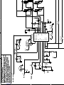
Linear Technology LTC3851EGN is a synchronous buck converter that provides high efficiency, low noise, and fast transient response. It operates over a wide input voltage range of 4.5V to 14V and can deliver up to 15A of continuous output current. The switching frequency is programmable from 100kHz to 2MHz, allowing for optimization of efficiency, size, and EMI. The LTC3851EGN also features a programmable soft-start function, output overvoltage protection, and thermal shutdown protection. Its applications include powering FPGAs, ASICs, DSPs, and other high-performance digital devices.
Linear Technology LTC3851EGN is a synchronous buck converter that provides high efficiency, low noise, and fast transient response. It operates over a wide input voltage range of 4.5V to 14V and can deliver up to 15A of continuous output current. The switching frequency is programmable from 100kHz to 2MHz, allowing for optimization of efficiency, size, and EMI. The LTC3851EGN also features a programmable soft-start function, output overvoltage protection, and thermal shutdown protection. Its applications include powering FPGAs, ASICs, DSPs, and other high-performance digital devices.


-
 1
1
-
 2
2
-
 3
3
-
 4
4
-
 5
5


Linear Technology LTC3851EGN is a synchronous buck converter that provides high efficiency, low noise, and fast transient response. It operates over a wide input voltage range of 4.5V to 14V and can deliver up to 15A of continuous output current. The switching frequency is programmable from 100kHz to 2MHz, allowing for optimization of efficiency, size, and EMI. The LTC3851EGN also features a programmable soft-start function, output overvoltage protection, and thermal shutdown protection. Its applications include powering FPGAs, ASICs, DSPs, and other high-performance digital devices.
Ask a question and I''ll find the answer in the document
Finding information in a document is now easier with AI
Related papers
-
Linear Technology LTC3202 User guide
-
Linear Technology DC1700A Demo Manual
-
-
-
-
-
-
-
-
Other documents
-
Linear DC1892A Demo Manual
-
Analog Devices Linear DC2681A-A Demo Manual
-
Analog Devices DC2383A-B User guide
-
Analog Devices DC2638A-C User manual
-
Analog Devices DC26 User manual
-
-
-
-
MICROCHIP ADM00845 Operating instructions
-
Analog Devices LTC3311 User guide