Page is loading ...

• output voltage stepless adjustment
• board size: 35×62 mm
• integrated voltmeter
• load capacity: up to 0.5A
Specifications
• ability to obtain two independent voltages on the
• supply voltage: 12÷24 VDC
Universal power supply to fit SD12NW prototype
boards and others with an internal pin lead spacing of
approximately 49mm. It provides for stepless
adjustment of the output voltage via a potentiometer.
The power supply, together with the prototyping
board, allows quick creation of projects without
soldering.
contact board
• integrated reverse polarity protection
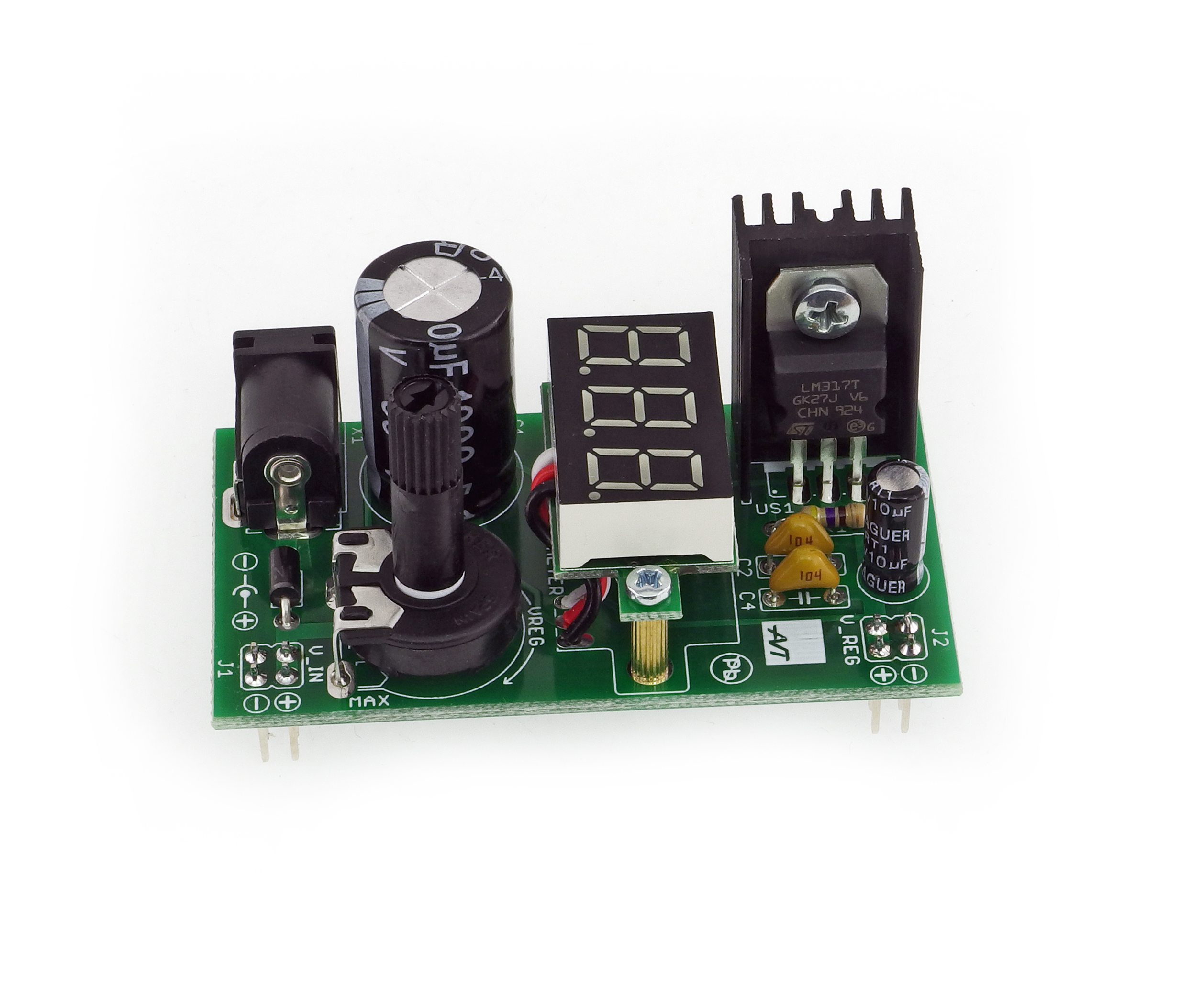
The diagram is shown in Figure 1. The actual voltage
stabiliser is the US1 integrated circuit. It is the well-
known LM317 chip. It works here in its basic
application layout and therefore does not require a
detailed description of the operating principle. A
significant advantage of the stabiliser used is that the
output is short-circuit-proof to earth and thermally
protected against overheating. These safeguards will
guarantee long and trouble-free operation in any
electronic technician's workshop. The output voltage
of the power supply is adjustable with potentiometer
PR1 over a very wide range. Not to complicate the
circuit, an adjustment potentiometer was used in the
form of a single potentiometer with a convenient
adjustment shaft. The power supply circuit can be
used at voltages up to 24 V and currents up to 500
mA. The voltmeter used is a universal module for
measuring voltages in the range 0V - 99.9 V and is
powered by 3 V - 30 V, in this case the input voltage
of the power supply.
Circuit description
Adjustable Power Supply
for Contact Boards
AVT 1990
1
ASSEMBLY DIFFICULTY
kits
PDF
DOWNLOAD
ZOOM

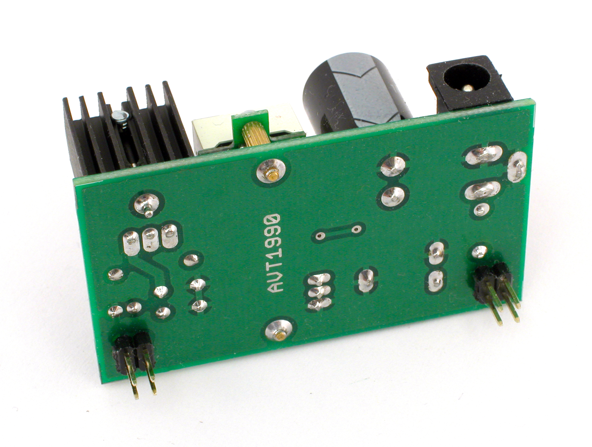
Printed circuit design is shown in Figure 2. Power
supply board size is 35 x 62 mm. Typical printed
circuit mounting that requires no further explanation.
The board is double-sided mainly due to the goldpin
mounting of the J1 and J2 connectors on the soldered
side. If they were only soldered on the underside of
the board, after several insertions and removals of the
power supply from the contact board, the solder
points would be torn out which would damage the
board. By soldering through two layers and
metallizing in between, the power supply board will
be much more resistant to damage. The stabiliser
radiator is also soldered to the board, which will avoid
bending the chip feet. The power supply board is
designed to work with SD-12NW contact boards, but
it is important to know that different versions of
prototype boards are commercially available with
different supply rail spacing.
The MOD1 voltmeter will either have wires attached
to it or it will have no wires, depending on the
version. In this case, add three sections of e.g., silver
or kynar. To secure it to the module board, fasten it
with M2 screws to two sleeves with an internal thread
on one side and an external thread on the other, as in
the model in the photos. The spacer sleeves with
external threads, mounted on the board, can be
additionally soldered - they are made of brass, which
is easily soldered. To make it easier to determine the
polarity of the J1, J2 and X1 connectors, the
descriptive layer includes + and - symbols, as well as
a symbol for the internal structure of the DC
connector.
Mounting and start-up
Figure 1. Schematic diagram of the contact board power supply
Figure 2. Contact board power supply mounting diagram
2x22x2
DC2.1/5.5
470
1000u
10u
1N5817
100n
10k
LM317
0330x
100n
V+ V+
GND
1 2
3 4
J2
1 2
3 4
J1
3
2
1
X1
R1
C1
C3
D1
C2
PR1
ADJ
IN OUT
US1
IN
Z+
Z-
MOD1
C4
+
+
ZOOM
2

List of elements
Mounting elements
C1: .............................1000 μF !
C3: .............................10 μF !
US1: ..........................LM317 !
X1: ............................ DC 2.1/5.5 socket
Resistors:
Capacitors:
Semiconductors:
MOD1: .................... voltmeter module 0330x (any colour)
H1:.............................radiator DY-CN
D1:.............................1N5817 ! or similar
C2, C4:......................100 μF (can be labelled 104)
J1, J2: .......................goldpin 2×2
R1: .............................470 Ω
PR1:...........................10 kΩ + adjustment shaft
Other:
Begin assembly by
soldering the
components onto the
board in order of size from
smallest to largest. When
mounting components
marked with an exclamation
mark, pay attention to their polarity.
Photographs of the assembled kit may be
helpful. To access high-resolution images,
download the PDF.
!
ZOOM
ZOOM
3
PDF
DOWNLOAD

Notes
4
AVT SPV reserves the right to make changes without prior notice.Installation and connection of the appliance not in accordance with the instructions, unauthorised modification of
components and any structural alterations may cause damage to the appliance and endanger persons using it. In such a case, the manufacturer and its authorised representatives shall
not be liable for any damage arising directly or indirectly from the use or malfunction of the product.
The self-assembly kits are intended for educational and demonstration purposes only. They are not intended for use in commercial applications. If they are used in such applications, the
purchaser assumes all responsibility for ensuring compliance with all regulations
This symbol means do not dispose of your
product with your other household waste.
Instead, you should protect human health
and the environment by handing over your
waste equipment to a designated collection
point for the recycling of waste electrical
and electronic equipment.
Leszczynowa 11 Street,
03-197 Warsaw, Poland
https://sklep.avt.pl/
AVT SPV Sp. z o.o.
kits
/