
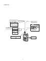
S-13903MZ-C1
2002 Icom Inc.
1-1-32, Kamiminami, Hirano-ku, Osaka 547-0003, Japan
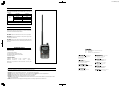
MULTIBAND FM TRANSCEIVER
iC-t90a
iC-t90a
IC-T90A (1,4)

INTRODUCTION
This service manual describes the latest service information for
the IC-T90A MULTIBAND FM TRANSCEIVER at the time of
publication.
T90A
U.S.A.
General
Canada
S.E. Asia
USA
GEN
CAN
SEA
To upgrade quality, all electrical or mechanical parts and inter-
nal circuits are subject to change without notice or obligation.
DANGER
NEVER connect the transceiver to an AC outlet or to a DC
power supply that uses more than 12 V. Such a connection
could cause a fire hazard and/or electric.
DO NOT expose the transceiver to rain, snow or any liquids.
DO NOT reverse the polarities of the power supply when
connecting the tranceiver.
DO NOT apply an RF signal of more than 20 dBm (100 mW)
to the antenna connector. This could damage the transceiver s
front end.
ORDERING PARTS
Be sure to include the following four points when ordering
replacement parts:
1. 10-digit order numbers
2. Component part number and name
3. Equipment model name and unit name
4. Quantity required
<SAMPLE ORDER>
1130006220 S.IC TC4W53FU IC-T90A LOGIC UNIT 1 piece
8930054290 2372 Main seal IC-T90A Chassis 5 pieces
Addresses are provided on the inside back cover for your
convenience.
REPAIR NOTES
1. Make sure a problem is internal before disassembling the transceiver.
2. DO NOT open the transceiver until the transceiver is disconnected from its power source.
3. DO NOT force any of the variable components. Turn them slowly and smoothly.
4. DO NOT short any circuits or electronic parts. An insulated tuning tool MUST be used for all adjustments.
5. DO NOT keep power ON for a long time when the transceiver is defective.
6. DO NOT transmit power into a signal generator or a sweep generator.
7. ALWAYS connect a 40 dB or 50 dB attenuator between the transceiver and a deviation meter or spectrum analyser when
using such test equipment.
8. READ the instructions of test equipment thoroughly before connecting equipment to the transceiver.
Communication Equipment
Himmelgeister Str. 100, D-40225 D sseldorf, Germany
Phone: 0211 346047 Fax : 0211 333639
URL : http://www.icomeurope.com
Unit 9, Sea St., Herne Bay, Kent, CT6 8LD, U.K.
Phone: 01227 741741 Fax : 01227 741742
URL : http://www.icomuk.co.uk
Zac de la Plaine, Rue Brindejonc des Moulinais
BP 5804, 31505 Toulouse Cedex, France
Phone: 561 36 03 03 Fax : 561 36 03 00
URL : http://www.icom-france.com
Crta. de Gracia a Manresa Km. 14,750
08190 Sant Cugat del Valles Barcelona, SPAIN
Phone: (93) 590 26 70 Fax : (93) 589 04 46
URL : http://www.icomspain.com
<
Corporate Headquarters
>
2380 116th Avenue N.E., Bellevue, WA 98004, U.S.A.
Phone: (425) 454-8155 Fax : (425) 454-1509
URL : http://www.icomamerica.com
<
Customer Service
>
Phone: (425) 454-7619
Glenwood Centre #150-6165
Highway 17 Delta, B.C., V4K 5B8, Canada
Phone: (604) 952-4266 Fax : (604) 952-0090
URL : http://www.icomcanada.com
A.B.N. 88 006 092 575
290-294 Albert Street, Brunswick, Victoria, 3056, Australia
Phone: 03 9387 0666 Fax : 03 9387 0022
URL : http://www.icom.net.au
146A Harris Road, East Tamaki,
Auckland, New Zealand
Phone: 09 274 4062 Fax : 09 274 4708
URL : http://www.icom.co.nz 6F No. 68, Sec. 1 Cheng-Teh Road, Taipei, Taiwan, R.O.C.
Phone: (02) 2559 1899 Fax : (02) 2559 1874
1-1-32, Kamiminami, Hirano-ku, Osaka 547-0003, Japan
Phone : 06 6793 5302
Fax : 06 6793 0013
URL : http://www.icom.co.jp/world/index.html
MODEL VERSION SYMBOL
IC-T90A (2,3)

TABLE OF CONTENTS
SECTION 1 SPECIFICATIONS
SECTION 2 INSIDE VIEWS
SECTION 3 DISASSEMBLY INSTRUCTIONS
SECTION 4 CIRCUIT DESCRIPTION
4 - 1 RECEIVER CIRCUITS ................................................................................................... 4 - 1
4 - 2 TRANSMITTER CIRCUITS ............................................................................................ 4 - 4
4 - 3 PLL CIRCUITS................................................................................................................. 4 - 5
4 - 4 POWER SUPPLY CIRCUITS.......................................................................................... 4 - 7
4 - 5 PORT ALLOCATIONS..................................................................................................... 4 - 7
SECTION 5 ADJUSTMENT PROCEDURES
5 - 1 PREPARATION................................................................................................................ 5 - 1
5 - 2 TRIMMER ADJUSTMENT............................................................................................... 5 - 3
5 - 3 ADJUSTMENT MODE ADJUSTMENTS ......................................................................... 5 - 5
SECTION 6 PARTS LIST
SECTION 7 MECHANICAL PARTS AND DISASSEMBLY
SECTION 8 SEMI-CONDUCTOR INFORMATION
SECTION 9 BOARD LAYOUTS
9 - 1 LOGIC UNIT.................................................................................................................... 9 - 1
9 - 2 RF UNIT........................................................................................................................... 9 - 3
9 - 3 AF UNIT / VCO UNIT ...................................................................................................... 9 - 5
SECTION 10 BLOCK DIAGRAM
SECTION 11 VOLTAGE DIAGRAM

1 - 1
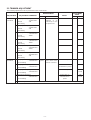
MGENERAL
• Frequency range : (Unit: MHz)
*1Specifications guaranteed 144 – 148 MHz
*2Specifications guaranteed 440 – 450 MHz
*3Specifications guaranteed 430 – 440 MHz
*4Except 824 – 849 MHz, 869 – 894 MHz [USA] only
• Mode : FM, AM (RX only) and WFM (Rx only)
• Number of memory channels : 555 (incl. 50 scan edges and 5 call channels)
• Frequency stability : ±6 ppm max. (–10˚C to +60˚C; 14˚F to 140˚F)
• Tuning steps : 5, 6.25, 8.33, 9, 10, 12.5, 15, 20, 25, 30, 50 100, and 200 kHz
• Usable tempareture range : –10˚C to +60˚C; 14˚F to 140˚F
• Power supply requirement : 5.5 – 11 V DC or specified battery pack
• Usable battery pack/case : BP-217 (7.4 V) and BP-216 (3.2 V)
• Polarity : Negative ground
• Current drain (at 8.0 V DC) : (typical value)
*1Power save duty is 1:4.
• Anntena connector : SMA (50 Ω)
• Dimensions
(projections not included)
: 58(W) ×87(H) ×29(D) mm;
217⁄32(W) × 37⁄16(H) × 15⁄32(D) in
• Weight (with BP-217/Ant.) : 280 g; 9
7⁄8
oz
MTRANSMITTER
• Output power (at 8.0 V DC) : High 5.0 W typical
Low 0.5 W typical
• Modulation system :
Variable reactance modulation
• Max. freq. deviation : ±5 kHz
• Spurious Emissions : Less than –60 dB
• External MIC connector : 3-conductor 2.5(d) mm (1⁄8”); 2 kΩ
SECTION 1 SPECIFICATIONS
440 MHz
2.0 A
1.2 A
RX
High power
Low power
Rated output
Standby
Power saved*1
50/145 MHz
2.0 A
0.8 A 220 mA
100 mA
65 mA
Version
USA
CAN
GEN
SEA
50 MHz
50 – 53.995
145 MHz
144 – 148
136 – 174*1
140 – 150*1
440 MHz
430 – 450*2
400 – 470*3
430 – 440
Receiving
0.495–999.990*4
TX

1 - 2
All stated specifications are subject to change without notice or obligation.
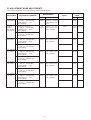
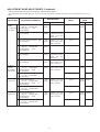
MRECEIVER
• Receiver system :
Double-conversion superheterodyne
• Intermediate frequency : 1st 13.350 MHz (FM/AM)
13.350 MHz (WFM)
2nd 450 kHz
• Sensitivity*1:
(except spurious points; typical values)
*1FM and WFM are measured at 12 dB SINAD, AM is mea-
sured at 10 dB S/N.
*2The frequency range is between 222.000 MHz and
229.995 MHz.
*3The frequency range is between 320.000 MHz and
329.995 MHz.
*4The frequency range is between 40.000 MHz and 108.000
MHz.
• Selectivity
AM and FM : Less than 15 kHz/–9 dB
More than 30 kHz/–60 dB
WFM : Less than 350 kHz/–3 dB
More than 700 kHz/–20 dB
• Spurious and image rejection ratio
: • 50 MHz More than 60 dB
IF/2: More than 50 dB
IF: More than 40 dB
• 145 MHz More than 60 dB
IF/2: More than 50 dB
• 440 MHz More than 50 dB
IF: More than 60 dB
• Audio output power : 200 mW typical at 10 % distor-
tion with an 8 Ωload
• AF output impedance : 8 Ω
• Squelch sensitivity*1: (typical; Except sprious points)
*1FM and WFM are measured at 12 dB SINAD, AM is mea-
sured at 10 dB S/N.
*2The frequency range is between 222.000 MHz and
229.995 MHz.
*3The frequency range is between 320.000 MHz and
330.000 MHz.
*4The frequency range is between 40.000 MHz and 108.000
MHz.
Frequency (MHz)
0.495–1.625
1.625–4.995
5.000–29.995
29.995–49.995
50.000–54.000
54.005–76.000
76.000–108.000
108.000–118.000
118.000–136.000
136.000–143.995
144.000–148.000
148.005–175.000
175.000–221.995
222.000–225.000
225.005–246.995
247.000–329.995
329.995–429.995
430.000–450.000
450.005–470.000
470.000–770.000
770.000–832.995
833.000–999.990
FM
–
0.4 µV
0.18 µV
0.16 µV
0.18 µV
0.16 µV
0.4 µV
0.32 µV
0.4 µV
0.32 µV
0.16 µV
0.32 µV
1.0 µV
AM
1.3 µV
0.56 µV
–
0.5 µV
–
0.79 µV*2
1.0 µV*3
–
WFM
–
1.0 µV*4
–
1.8 µV
–
3.2 µV
–
Frequency (MHz)
0.495–1.625
1.625–4.995
5.000–29.995
29.995–49.995
50.000–54.000
54.005–76.000
76.000–108.000
108.000–118.000
118.000–136.000
136.000–143.995
144.000–148.000
148.005–175.000
175.000–221.995
222.000–225.000
225.005–246.995
247.000–329.995
329.995–429.995
430.000–450.000
450.005–470.000
470.000–770.000
770.000–832.995
833.000–1319.995
FM
–
0.4 µV
0.18 µV
0.16 µV
0.18 µV
0.16 µV
0.4 µV
0.32 µV
0.4 µV
0.32 µV
0.16 µV
0.32 µV
1.0 µV
AM
1.3 µV
0.56 µV
–
0.5 µV
–
0.79 µV*2
1.0 µV*3
–
WFM
–
1.0 µV*4
–
1.8 µV
–
3.2 µV
–

2 - 1
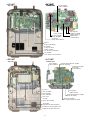
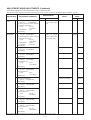
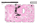
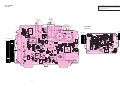
SECTION 2 INSIDE VIEWS
EEPROM
(IC2: HN58X24128FPI,
Q2: UN9115)
RESET IC
(IC142: S-80928CNMC) Crystal oscillator for CPU clock
(X1: CR-687, 6.7584 MHz, Q40: UN9215)
CPU
(IC1: M30220MA-114RP)
AF regulator
(Q201: 2SB1201,
Q202: XP1501)
+3 regulator
(Q8: 2SB1132,
Q9: XP1501)
+3C regulator
(Q142: XP1501,
Q145: 2SB1132,
D143: MA2S111)
CPU3 regulator
(IC141: NJM2370U32)
440 MHz band modulation switch
(Q304: 2SJ364)
Microphone mute
(Q310: XP6501)
Microphone amplifier
(Q311: XP5601,
Q312: XP6501) 145 MHz band modulation switch
(Q305: 2SJ364)
50 MHz band modulation switch
(Q342: 2SJ364)
• LOGIC UNIT
Top view • LOGIC UNIT
Bottom view

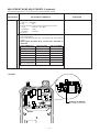
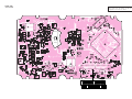
2 - 2
50 MHz TX low-pass filter circuit
144 MHz TX high-pass filter circuit
Pre-drive
(Q54: 2SC5289)
Drive amplifier
(Q52: 2SK3475)
0.495–29.995 MHz RF amplifier
(Q302: 2SC5006)
75.995–229.995 MHz
RF amplifier
(Q351: 3SK320)
R3 regulator
(Q353: XP4312)
29.995–75.995 MHz
RF amplifier (Q303: 2SC5006)
629.995–999.90 MHz RF amplifier
(Q452: 2SK3475)
T3 regulator
(Q56: XP4315, D50: MA6S121)
1st mixer
(IC351: µPC2757TB)
VCO circuit
Power amplifier
(Q51: 2SK3476)
FM IF IC
(IC151: TA31136FN)
1st AF amplifier
(Q205: 2SD2216)
AF mute
(Q251: 2SJ364)
IF amplifier
(Q102: 2SC4403)
T5V regulator
(Q11: XP1501, Q55: 2SB1132)
Crystal oscillator
(X1: VR-583, 13.800 MHz)
AF power amplifier
(IC252: TA7368F) AM/FM switch
(Q206: XP4315)
R3V regulator
Q208: 2SA1576
Q209: XP1501
AM detector
(Q201, Q202: XP6501)
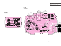
• AF UNIT
Top view
• RF UNIT
Top view
• AF UNIT
Bottom view
• AF UNIT
Bottom view
• RF UNIT
Bottom view

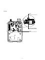
3 - 1
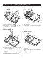
SECTION 3 DISASSEMBLY INSTRUCTIONS
1. Removing the rear panel
2. Removing the LOGIC unit
3. Removing the AF unit
4. Removing the RF unit
qUnscrew 1 screw A(M2 ×4 mm, black).
wUnscrew 2 screws B(M2 ×20 mm, black), and 4 screws
C(M2 ×6 mm, black) from the rear panel.
eTake off the rear panel in the direction of the arrow.
qUnplug the flexible cable W1 from J1 on the LOGIC unit
to separate the rear panel.
wTake off the main seal.
eUnsolder 2 points Dat the speaker lead.
rUnscrew 6 screws E(2 ×4 mm, silver) to separate the
LOGIC unit.
NOTE:
When you tighten 6 screws E, tighten those in turn of 1–6.
qTake off the lock plate.
wUnsolder 5 points Fat the antenna plate, vol plate and
lead.
eUnscrew 1 screw G(2 ×4 mm, silver), and 2 screws H
(M2 ×12 mm, black) from the AF unit.
rTake off the AF unit in the direction of the arrow to sepa-
rate the rear panel.
qUnsolder 2 points I at the antenna rug plate and anten-
na connector.
wUnscrew 2 screws J(M2 ×4 mm, silver) from the FRONT
panel.
eTake off the RF unit in the direction of the arrow to sepa-
rate the rear panel.
Rear panel
A
B
C
W1 (L)
J1 Main seal
E
E
2
3
4
5
LOGIC unit
1
6
D
G
J251
Lock plate
Rear panel
AF unit
Vol plateVol lead
Antenna
plate
F
F
F
H
J
RF unit
Antenna rug
Antenna
connector
Rear panel
I

SECTION 4 CIRCUIT DESCRIPTION
4 - 1
4-1 RECEIVER CIRCUITS
4-1-1 TRIPLEXER CIRCUIT (RF UNIT)
The transceiver has a triplexer (low-pass and bandpass fil-
ters) on the first stage from the antenna switching diode to
separate the signals.
• RF signals 0.495 MHz–75.995 MHz
The 0.495 MHz–75.995 MHz RF signals are passed through
the low-pass filters (L5, L6, L24, C43, C483–C486, L11–L13,
L17–L19, C21, C481, C482) and are applied to the antenna
switching circuit.
• RF signals 76.0 MHz–299.995 MHz
The 76.0 MHz–299.995 MHz RF signals are passed through
the low-pass (L5, L6, L24, C43, C483–C486) and high-pass
(L9, C9–C11) filters and are applied to the antenna switching
circuit.
• RF signals 230.0 MHz–629.995 MHz
The 230.0 MHz–629.995 MHz RF signals are passed
through the high-pass (L1, C1–C3) and low-pass (FI1) filters
and are applied to the antenna switching circuit.
• RF signals 630.0 MHz–999.990 MHz
The 630.0 MHz–999.990 MHz RF signals are passed
through the high-pass (L3, L4, C6–C8) filter and are applied
to the RF circuit.
4-1-2 ANTENNA SWITCHING CIRCUIT (RF UNIT)
The antenna switching circuit functions as a low-pass filter
while receiving. However, its impedance becomes very high
while transmitting by applying a current to D4, D6, D9, D12,
D13, D19.
Thus, tramsmit signals are blocked from the entering the
receiver circuits. The antenna switching circuit employs a
1/4λtype diode switching system. The signals are applied to
the each antenna switching circuit.
• RF signals 0.495 MHz–75.995 MHz
The signals pass through the antenna switching circuit (D9),
and then applied to the RF circuit.
• RF signals 76.0 MHz–299.995 MHz
The signals pass through the antenna switching circuit (D8),
and then applied to the RF circuit.
• RF signals 230.0.0 MHz–629.995 MHz
The signals pass through the antenna switching circuit (D7),
and then applied to the RF circuit.
4-1-3 RF CIRCUIT (RF UNIT)
The RF circuit amplifies the received signals within the range
of frequency coverage and filters out-of-band signals.
(1) 0.495 MHz–29.995 MHz RF CIRCUIT
The signals from the antenna switching circuit pass through
the attenuator (D305) and band switch (D301). The signals
applied to the bandpass filter (L301, L302, C301–C307) to
suppress unwanted signals, then amplified at the RF amplifi-
er (Q302).
(2) 30.0 MHz–75.995 MHz RF CIRCUIT
The signals from the antenna switching circuit pass through
the attenuator (D305) and band switch (D306). The signals
applied to the bandpass filter (D307, D308, L303, L304,
C317–C320) to suppress unwanted signals, then pass
through the bandpass filter (D309, D310, L306, L307,
L323–C325, C331) after being amplified at the RF amplifier
(Q303).
ANT
LPF
LPF
ATT
CTRL
HPF
HPF
HPF
LIMIT
LIMIT
ANT
SW
LPF
ANT
SW
ANT
SW
LIMIT
LIMIT SW
SW
75.995 MHz RF signals
299.995 MHz RF signals
629.995 MHz RF signals
999.990 MHz RF signals
0.495 MHz
76.0 MHz
230.0 MHz
630.0 MHz
R3V
Q355 Antenna
switching
circuit Triplexer
circuit
D305
D351
D401
D451
D6, D9
D4, D19
D12, D13
D457
D10
ATT
• TRIPLEXER AND ANTENNA SWITCHING CIRCUITS

4 - 2
(3) 76.0 MHz–229.995 MHz RF CIRCUIT
The signals from the antenna switching circuit pass through
the attenuator (D351), and then applied to the bandpass fil-
ter (D352, D353, L351, L352) to suppress unwanted signals.
The signals pass through the bandpass filter (D354–D356,
D359, L354, L355, L357, L358, C357–C364) after being
amplified at the RF amplifier (Q351).
(4) 230.0 MHz–629.995 MHz RF CIRCUIT
The signals from the antenna switching circuit are applied to
the band switch (D457), and then pass through the attenua-
tor (D401). The signals pass through the bandpass filter
(D402, D403, L401, L402, C402, C404–C406) to suppress
unwanted signals, then applied to the RF amplifier (Q401).
The amplified signals pass through the bandpass filter
(D405, D407, L409, C414, C415), and are then amplified at
the RF amplifier (Q402).
(5) 630.0 MHz–999.990 MHz RF CIRCUIT
The signals from the antenna pass through the high-pass fil-
ter (L3, L4, C6–C8), and then applied to the attenuator
(D451) after being passed through the band switch (D10).
The signals pass through the bandpass filter (D452, L451,
C451–C454), then applied to the RF amplifier (Q451). The
amplified signals pass through the bandpass filter (D453,
D454, L452, L453, C456, C460, C462–C464) and RF ampli-
fier (Q452).
The amplified or filtered signals pass through one of the band
switch (D303, D313, D358, D408, D455), and then applied to
the 1st mixer circuit (IC351, pin 1).
4-1-4 1ST MIXER AND 1ST IF CIRCUITS (RF, AF
AND VCO UNITS)
The 1st mixer circuit converts the received RF signals to a
fixed frequency of the 1st IF signal with a PLL output fre-
quency. By changing the PLL frequency, only the desired fre-
quency will pass through the bandpass filter at the next stage
of the 1st mixer.
The amplified or filtered RF signals are mixed with 1st LO
signals at the 1st mixer (IC351) to produce a 69.45 MHz 1st
IF signal. The 1st IF signal is output from pin 6, and passed
through the bandpass filter (Narrow: AF unit; FI101, Wide: AF
unit; FI102) to suppress unwanted harmonic components via
the mode switch (AF unit; D101, D102). The filtered 1st IF
signal is applied to the IF amplifier (AF unit; Q102). The
amplified signal is applied to the 2nd mixer circuit.
The 1st LO signals (53.350 MHz–99.345 MHz, 99.350
MHz–560.545 MHz or 281.675 MHz–534.720 MHz) are gen-
erated at the 144 MHz VCO (VCO unit; Q3–Q5, D3, D4) or
430 MHz VCO (VCO unit; Q1, Q2, D1) circuits. The oscillat-
ed signal is applied to the 1st mixer via the doubler circuit
(Q354, D357) or directly.
4-1-5 2ND IF AND DEMODULATOR CIRCUITS
(AF UNIT)
The 2nd mixer circuit converts the 1st IF signal to a 2nd IF
signal. A double conversion superheterodyne system (which
converts receive signals twice) improves the image rejection
ratio and obtain stable receiver gain.
The FM IF IC (IC151) contains 2nd local oscillator, 2nd mixer,
limiter amplifier, quadrature detector and S-meter detector
circuits.
The amplified 69.45 MHz 1st IF signal from the IF amplifier
(Q102) is mixed with the 2nd LO signal at the 2nd mixer
(IC151) to produce a 455 kHz 2nd IF signal. The 2nd IF sig-
nal from the IC151, pin 3 passes through (AM and FM mode)
or bypasses (WFM mode) the 2nd IF filter (FI151) where
unwanted heterodyne signals are suppressed via the mode
switch (D151, D152). The filtered signals are applied to the
AM detector circuit or FM detector circuit respectively.
RF
RF
SW
SW
SW
BPF
BPF
BPF
RF
SW BPF
BPF
RF
RF
SW BPF
BPF
RF
RF
SW BPFBPF
0.495 MHz 75.995 MHz
RF signals
1st LO signal
from the VCO circuit
Q401
Q451
Q402
Q452
Q351
Q302
D303
D313
D358
D408
D455
D301,
D306
Q303
1st mixer
(IC351)
1st IF signal to the AF unit
(AM, FM: 69.45 MHz,
WFM: 13.35 MHz)
76.0 MHz 299.995 MHz
RF signals
230.0 MHz 629.995 MHz
RF signals
630.0 MHz 999.990 MHz
RF signals
"AGC" signal from
the AF unit (Q202, pin 4)
• RF CIRCUIT

4 - 3
(1) AM DETECTOR CIRCUIT
The filtered signals are applied to the AM detector circuit
(Q201, Q202) to demodulate the 2nd IF signal into the AM AF
signals.
(2) FM AND WFM DETECTOR CIRCUIT
The filtered signals are applied to the limiter amplifier section
in the FM IF IC (IC151, pin 5), and then applied to the quad-
rature detector section to demodulate the 2nd IF signal into
FM and WFM AF signals.
The demodulated AM, FM or WFM signals are applied to the
AF amplifier circuit.
4-1-6 AF AMPLIFIER CIRCUIT (AF UNIT)
The AF amplifier circuit which is included a low-pass filter, AF
mute switch, AF volume controller and AF amplifier amplifies
the demodulated AF signals to drive a speaker.
(1) AM AND FM AF SIGNALS
The demodulated AM or FM (“DETO” signal) AF signals from
the AM detector (Q201, Q202) or FM detector (IC151, pin 9)
circuits are passed through the low-pass filter (Q204) via the
mode swtich (D201). The filtered signals are applied to the
1st AF amplifier (Q205).
(2) WFM AF SIGNALS
The demodulated WFM (“DETO” signal) AF signals from FM
detector (IC151, pin 9) circuit are bypassed the low-pass fil-
ter (Q204) via the mode swtich (D201). The demodulated
signals are applied to the 1st AF amplifier (Q205).
The amplified AF signals from the 1st AF amplifier (Q205) are
applied to the AF mute switch (Q251) which is controlled by
“MUTE” signal from the CPU (LOGIC unit; IC1, pin 48), and
are then applied to the electronic volume control circuit
(IC251, pin 6). The level controlled AF signals are output
from the volume IC (LOGIC unit; IC251, pin 7) and are then
applied to the AF power amplifier (IC252, pin 4). The power
amplified AF signals are then applied to the internal speaker
(LOGIC unit; SP1) through the “INTSP” signal via the [EXT
SP] jack (J253) when no plug is connected to the jack.
The AF filter circuit (LOGIC unit; IC241, pin 5) removes AF
signals below 300 Hz (CTCSS signals) for clear AF output
and these are applied to the CPU (LOGIC unit; IC1, pin 7) for
the CTCSS squelch detection via the “CTCIN” line.
The electronic volume control circuit controls AF gain, there-
fore, the AF output level is according to the [VOL] setting and
also the squelch conditions.
4-1-7 SQUELCH CIRCUIT(AF AND LOGIC UNITS)
• NOISE SQUELCH
The noise squelch circuit cuts out AF signals when no RF sig-
nals are received. By detecting noise components in the AF
signals, the squelch circuit switches the AF mute switch.
A portion of the AF signals from the FM IF IC (IC151, pin 9)
are applied to the active filter section (IC151, pins 7, 8). The
active filter section amplifies and filters noise components.
The filtered signals are applied to the noise detector section
and output from IC151 (pin 13) as the “NOISE” signal.
The “NOISE” signal from IC151 (pin 13) is applied to the CPU
(LOGIC unit; IC1, pin 47). The CPU analyzes the noise con-
dition and outputs the “MUTE” signal to AF mute switch
(Q251).
Even when the squelch is closed, the AF mute switch (Q251)
opens at the moment of emitting beep tones.
• TONE SQUELCH
The tone squelch circuit detects AF signals and opens the
squelch only when receiving a signal containing a matching
subaudible tone (CTCSS). When tone squelch is in use, and
a signal with a mismatched or no subaudible tone is
received, the tone squelch circuit mutes the AF signals even
when noise squelch is open.
A portion of the AF signals from the FM IF IC (IC151, pin 9)
passes through the low-pass filter (LOGIC unit; IC241, pins
5, 7) to remove AF (voice) signals and is applied to the
CTCSS decoder inside the CPU (LOGIC unit; IC1, pin 8) via
the “CTCIN” line to control the AF mute switch.
Mixer
16
Limiter
amp.
2nd IF filter
450 kHz
RSSI
IC151 TA31136FN
13 1st IF (69.45 MHz)
from IC351, pin 6 (RF unit)
"SD" signal to the CPU
pin 3
11
10
9
875 3
2
Active
filter
FI151
Noise
detector
FM
detector Noise
comp.
"NOISE" signal to the CPU
pin 48
12
C154
C160 C161
C158
R167
R159
Q201,
Q202
R158
"DETO" signal to the low-pass
filter (LOGIC unit; IC241)
AF signal to the mode switch
(AF unit; Q203, D201)
2nd
Q207
R3VWFM
"2nd LO" signal from
X1 (RF unit)
C156
R155
R151
C155
AM
detector
WFM
CTRL
• 2ND IF AND DEMODULATOR CIRCUIT

4 - 4
4-1-8 AGC CIRCUIT (AF AND RF UNITS)
The AGC (Automatic Gain Control) circuit reduce signal fad-
ing and keeps the audio output level constant.
A portion of AF signals from the AM detector circuit (Q201)
are applied to the amplifier (Q202). The amplified DC voltage
from the Q202, pin 4 is applied to the RF amplifiers (RF unit;
Q302, Q303, Q351, Q401, Q402, Q451, Q452) to reduce the
amplifier gain when strong signals are received.
4-2 TRANSMITTER CIRCUITS
4-2-1 MICROPHON AMPLIFIER CIRCUIIT
(LOGIC UNIT)
The microphone amplifier circuit amplifies the audio signals
from the microphone, within +6 dB/octave pre-emphasis
characteristics (300 Hz–3 kHz), to a level needed for the
modulation circuit. The microphone amplifier circuit is used
for both the VHF and UHF bands.
The AF signals from the microphone (MC1) or external [MIC]
jack (AF unit; J252) passes through the microphone mute cir-
cuit (Q310, pins 4, 2) which is controlled by the CPU (IC1, pin
48) via the “MUTE” signal. The AF signals are applied to the
microphone (limiter) amplifier (Q311, Q312) which has +6
dB/octave pre-emphasis characteristics, and are then
passed through the low-pass filter (Q310, pins 4, 1). The fil-
tered signals are applied to the modulation circuit (VCO unit)
as the “VMOD” signal via the each modulation band switch
(Q342, R365: for 50 MHz band, Q305, R326: for 145 MHz
band, Q304, R325: for the 440 MHz band).
4-2-2 MODULATION CIRCUIT (RF AND VCO UNITS)
The modulation circuit modulates the VCO oscillating signal
(RF signal) using the microphone AF signals.
The signals from the modulation band switches (LOGIC unit)
are then applied to the 144 MHz VCO or 430 MHz VCO cir-
cuits separately.
• 144 MHz VCO
The applied signals from the RF unit change the reactance of
D3 to modulate the oscillated signal at the 144 MHz VCO cir-
cuit (VCO unit; Q4, Q5).
• 430 MHz VCO
The applied signals from the RF unit change the reactance of
D1 to modulate the oscillated signal at the 430 MHz VCO cir-
cuit (VCO unit; Q1, Q2).
The modulated signal is amplified at the buffer amplifier
(VCO unit; Q7) and is then bypassed divider circuit (VCO
unit; IC1) via the divier switch (VCO unit; D8, D10). The sig-
nal is amplified at the two LO amplifiers (VCO unit; Q16,
Q212), and then applied to the drive/power amplifier circuits.
4-2-3 DRIVE/POWER AMPLIFIER CIRCUITS
(RF UNIT)
The drive amplifier circuit amplifies the transmit signal to a
level needed for the power amplifier circuit. The power ampli-
fier circuit amplifies this to obtain a specified transmit output
power.
The signal from the two LO amplifiers (VCO unit; Q16, Q212)
is passed through the Transmit/Receive switch (Q51), and is
amplified at the buffer amplifier (IC51, pin 1). The signal is
applied to the pre-driver (Q54) via the attenuator (D54). The
amplified signal is applied to the power amplifier via the 50
MHz line, 144 MHz and 430 MHz line separetly.
• 50 MHz LINE
The amplified signal passes through the low-pass filter (L54,
C60, C89, R81, R82) via the D57, and is then applied to the
power amplifier (Q51).
• 144 MHz AND 430 MHz LINE
The amplified signal passes through the high-pass filter (L56,
C65, C68, C69), and is then applied to the drive amplifier
(Q52). The signal is applied to the power amplifier (Q51).
The amplified signal is applied to the each TX filter circuit.
4-2-4 TX FILTER CIRCUIT (RF UNIT)
The amplified signal from the drive/power amplified circuit is
passed through the each TX filter circuit to suppress high-
harmonics spurious components
(1) 50 MHz TX FILTER CIRCUIT
The amplified 50 MHz signal from the power amplifier pass-
es through the low-pass filter (L22, L23, C34, C44, C480)
and 1/4λtype antenna switch (D6). The filtered signal is
applied to the low-pass filter (L11–L13, L17–L19, C21, C481,
C482) again, and is then passed through the triplexer circuit
(L5, L6, L24, C43, C483, C486).
(2) 144 MHz TX FILTER CIRCUIT
The amplified 144 MHz signal from the power amplifier pass-
es through the bandpass filter (L18, L19, C24, C26, C27) and
1/4λtype antenna switch (D4, D19). The filtered signal is
applied to the high-pass filter (L9, C9–C11), and is then
passed through the triplexer circuit (L5, L6, L24, C43,
C483–C486).
(3) 430 MHz TX FILTER CIRCUIT
The amplified 430 MHz signal from the power amplifier pass-
es through the high-pass filter (L16, L456, C32, C33, C98)
and 1/4λtype antenna switch (D2, D18). The filtered signal
is applied to the low-pass filter (FI1), and is then passed
through the triplexer circuit (L1, C1–C3).
The filtered signal is applied to the antenna connector
(CHASSIS unit; J1).
Collector voltage for the drive amplifier (Q52) and control
voltage for the power amplifier (Q51) are controlled by the
APC circuit to protect the power module from a mismatched
condition as well as to stabilize the output power.

4 - 5
4-2-5 APC CIRCUIT (RF UNIT)
The APC circuit protects the power amplifier from a mis-
matched output load and stabilizes the output power. The
APC circuit is designed to use VHF and UHF bands com-
monly.
The APC sensor (R109) detects driving current from the drive
voltage at the drive (Q52) and power (Q51) amplifiers. The
detected current is converted into DC voltage at Q101, then
applied to the APC control circuit (IC101, pin 2). The applied
voltage is compared with a “PSET” voltage from the CPU via
the D/A convertor (IC251), and the APC control circuit out-
puts control voltage from pin 1 to control the drive and power
amplifiers.
When the driving current is increased, input voltage of the dif-
ferential amplifier (IC101, pin 2) will be increased. In such
cases, the differential amplifier output voltage (IC101, pin 1)
is decreased to reduce the driving current.
4-3 PLL CIRCUITS
4-3-1 GENERAL
A PLL circuit provides stable oscillation of the transmit fre-
quency and the receive local frequency. The PLL circuit
compares the phase of the divided VCO frequency to the ref-
erence frequency. The PLL output frequency is controlled by
the divided ratio (N-data) of a programmable divider.
4-3-2 144 MHz AND 430 MHz VCO CIRCUITS
(VCO UNIT)
• 144 MHz VCO CIRCUIT
The oscillated signal at the 144 MHz VCO circuit (Q1–Q3,
D1, D2) is amplified at two buffer amplifiers (Q7, Q11), and is
then applied to the PLLIC (IC201, pin 19). The signal is divid-
ed by serial data from the CPU (LOGIC unit; IC1) and phase
detected with the divided reference frequency (5 kHz). The
phase difference is output from pin 5 as pulses.
Q102 Q101
TXC
VCC R109
APC SENSOR CIRCUIT
D/A CONVERTER
IC251
(RF unit)
+3
from Tx/Rx
switch
IC101
+
IC101
Differential
amplifier
1
7
2
36 PSET
514 DSET
VGGC
Pre
drive
Buff.
amp.
Power
amp.
Drive
amp.Q52
IC51 Q54
Q51 to the antenna
50 MHz
RF transmit signal
144, 430 MHz
RF transmit signal
• APC CIRCUIT

4 - 6
• 430 MHz VCO CIRCUIT
The oscillated signal at the 430 MHz VCO circuit (Q4, Q5,
D3) is amplified at two buffer amplifiers (Q7, Q11), and is
then applied to the PLLIC (IC201, pin 19). The signal is divid-
ed by serial data from the CPU (LOGIC unit; IC1) and phase-
detected with the divided reference frequency (5 kHz). The
phase difference is output from pin 5 as pulses.
The output signals from the PLL IC (IC201, pin 5) are con-
verted to DC voltages (lock voltage) by the loop filter, and are
then fed back to the 144 MHz and 430 MHz VCO circuits to
stabilize the VCO frequency.
4-3-3 VCO DIVIDER CIRCUIT (VCO AND RF UNITS)
The PLL circuit employs the two VCO circuits (144 MHz and
430 MHz) and VCO divider (IC1) to transmit on 3 bands and
receive wide band.
The oscillated signal at the 144 MHz or 430 MHz VCO circuit
is amplified at the buffer amplifier (Q7), and is then passed
through the divider switch (D7, D8).
When the signal is applied to the divider circuit (IC1, pin 2),
the circuit divides the VCO signal into the ratio of 1/2. The
divided signal passes through the low-pass filter (L12, L13,
C48–C51) and divider switch (D9).
When the signal bypasses the divider circuit (IC1), it passes
through the divider switch (D8, D10).
The VCO signal is applied to the LO amplifiers (Q16, Q212),
and then passed through the transmit/receive switch (D21,
D202). The signal is applied to the buffer amplifier (RF unit;
IC51, pin 1) for the TX LO frequency, or applied to the 1st
mixer circuit (IC351, pin 3) for the RX 1st LO frequency as
“LO” signal via or bypass the doubler circuit (Q354).
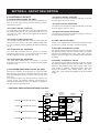
Shift register
Prescaler
Phase
detector
Loop
filter
Programmable
counter
PLL lock detector
Programmable
divider
X1
13.8 MHz
Q1, Q2,
D1
430 MHz VCO
50, 144MHz VCO Buff. Q11
Q7
D7
D8
D9
D10
Q206,
Q207
3
4PLSTB
IC201 (PLL IC)
AF UNIT
RF UNIT
CLK
7UNLK
to transmitter circuit
to 1st mixer circuit
(IC351, pin 3)
15
13 19
Q3, Q4,
Q5,
D3, D4
1/2 LPF
Buff.
Q16
LO
Q212
TX/RX
switch
D51
D201
LO
Q2 to FM IF IC (IC151, pin 2)
Amp.
Q211
Amp.
Buff.
Q1
• PLL CIRCUIT

4 - 7
LINE
HV
VCC
CPU3
+3C
+3
+10V
AFV
R3
R3V
T3
DESCRIPTION
The voltage from the external power supply or
attached battery pack.
The same voltage as the “HV” line (external
power supply or battery pack).
Common 3 V converted from the “VCC” line by
CPU3 regulator IC (LOGIC unit; IC141). The out-
put voltage is supplied to the +3C regulator cir-
cuits, etc.
Common 3 V converted from the “VCC” line by
the +3C regulator circuit (LOGIC unit; Q142 and
Q145) using the +3CPU regulator (LOGIC unit;
IC141.)
Common 3 V converted from the “VCC” line by
the +3 regulator circuit (LOGIC unit; Q8 and Q9)
using the +3C regulator (LOGIC unit; Q142 and
Q145).
Common 10 V converted from the “+3” line by
the +10 regulator circuit(LOGIC unit; IC91, IC92,
Q91, D91, D300–D302). The output voltage is
applied to the RF and VCO units.
6 V for receiver circuit converted from the “VCC”
line by the “AF” regulator circuit (LOGIC unit;
Q201, Q202). The output voltage is applied to
the AF amplifier (AF unit; IC252, pin 2).
3 V for receiver circuit converted from the “+3”
line by the “R3” regulator circuit (RF unit; O353).
3 V for the receiver circuit converted from the
“VCC” line by the “R3V’ regulator circuit (AF unit;
Q208 and Q209).
3 V for transmitter circuit converted from the “+3”
line by the “T3” regulator circuit (RF unit; Q56
and D20). The output voltage is applied to the
buffer amplifier (RF unit; IC51, pin 6).
4-4 POWER SUPPLY CIRCUITS
VOLTAGE LINE
Pin Port Description
number name
4
5
6
7
14
15
BSFT
B1C
B2C
B3
B4C
B5
Outputs frequency shift control signal
to tuned bandpass filters (RF unit).
Outputs 0.5–29.995 MHz band control
signal.
Low: While 0.5–29.995 MHz band is
receiving.
Outputs 30–75.995 MHz band control
signal.
Low: While 30–75.995 MHz band is
receiving.
Outputs 76–229.995 MHz band con-
trol signal.
Low: While 76–229.995 MHz band is
receiving.
Outputs 230–629.995 MHz band con-
trol signal.
Low: While 230–629.995 MHz band
is receiving.
Outputs 630–999.995 MHz band con-
trol signal.
Low: While 630–999.995 MHz band
is receiving.
Pin Port Description
number name
5
6
11
12
13
14
Outputs frequnecy setting D/A data to
the reference oscillator (RF unit; X1).
Outputs the power amplifier’s output
power setting data to the APC con-
troller (RF unit; IC101).
Outputs D/A data to the tuned band-
pass filters (RF unit).
Outputs the R3 regulator (RF unit;
Q353) control signal.
High:While receiving.
Outputs attenuator control signal.
Low: Attenuator is ON.
Outputs the drive amplifier’s output
power setting data to the APC con-
troller (RF unit; IC101).
FSET
PSET
TUNE
RXC
ATT
DSET
4-5-2 R3V SWITCH IC (AF UNIT; IC51)
4-5 PORT ALLOCATIONS
4-5-1 D/A CONVERTOR IC (RF UNIT; IC251)

4 - 8
Pin Port Description
number name Pin Port Description
number name
1
3
5
6
7
12
13
14
19
25
26
28
29
30
31
33
34
35
40
42
43
44
45
PATMP
SD
CHG
VIN
CTCIN
WFM
AM
CLSFT
RESET
POWER
CPUHV
IOSTB
DASTB
CLIN
CLOUT
PDAUL
CK
PLSTB
ECK
CHGC
PCON
R3C
TXC
Input port for the PA’s temperature
while transmitting.
Input port for the S-meter signal.
Input port for the battery voltage divide
signal.
Input port for the power supply voltage
divide signal.
Input port for the CTCSS decorded
signal (67.0–254.1 Hz analog signal).
Outputs the FM or WFM regulator
control signal.
Low: FM or WFM mode is selected.
Outputs the AM mode regulator con-
trol signal.
Low: AM mode is selected.
Outputs the clock shift control signal.
Input port for the CPU reset signal.
High:The CPU is reset.
Input port for the [POWER] switch.
Low: Power is ON.
Input port for the external power sup-
ply connecting signal.
Low: While the external power sup-
ply is connected.
Outputs the expander IC (AF unit;
IC51, pin 1) strobe signal.
Outputs strobe signals to the D/A IC
(RF unit; IC251, pin 2).
Input port for the cloning signal.
Output port for the cloning signal.
I/O port for the PLL IC (VCO unit;
IC201, pin 7) data signal.
Low: PLL is unlocked.
High:PLL is locked.
Outputs clock signals to the R3V
switch (AF unit; IC51, pin 3), D/A IC
(RF unit; IC251, pin 3) and PLL IC
(VCO unit; IC201, pin 4).
Outputs the PLL IC strobe signal.
Outputs the EEPROM clock signal.
Outputs the battery charger control
signal.
Outputs the +3C regulator control sig-
nal.
Outputs the R3C regulator control sig-
nal.
Low: While receiving.
Outputs the T5V regulator control sig-
nal.
High:While transmitting.
46
47
48
49
51
52
53
54
55
56
57
58–61
62–65
66–69
70
71
72
73
74
75
77
81
82
Outputs the mic amplifier regulator
control signal.
Input port for the SQL detection noise
signal.
Outputs mute control signal.
High:AF muting while receiving.
MIC muting while transmitting.
Output AF amplifier regulator control
signal.
Outputs BUSY LED control signal.
High:The BUSY LED is ON.
Outputs key backlight control signal.
High:Green backlight is ON.
Outputs key backlight control signal.
High:Red backlight is ON.
Outputs LCD backlight control signal.
Low: Lights ON.
Outputs the 430 MHz VCO regulator
control signal.
Low: 430 MHz is selected.
Input port for the up/down signal from
the main dial (AF unit; S251).
Output ports for key matrix.
Output ports for Initial matrix.
Input ports for key matrix.
Outputs the 50 MHz VCO regulator
control signal.
Low: 50 MHz is selected.
Input port for the volume level control
signal.
Low: Volume level is low.
Input port for the volume level control
signal.
Low: Volume level is high.
Input port for the [SQL] switch.
Low: While [SQL] switch is pushed.
Outputs the 430 MHz modulation cir-
cuit control signal.
Low: While 430 MHz is transmitting.
Outputs the 144 MHz modulation cir-
cuit control signal.
Low: While 144 MHz is transmitting.
Input port for the [PTT] switch.
High:While [PTT] switch is pushed.
Outputs 144 MHz VCO regulator con-
trol signal.
Low: 144 MHz is selected.
Outputs the VCO select signal.
MICC
NOISE
MUTE
AFON
BUSYL
GLED
RLED
LCDL
V3C
DIUD
DICK
KS3–KS0
I3–I0
KR3–KR1
V1C
VOLDN
VOLUP
SQL
430M
144M
PTT
V2C
VSFT
4-5-3 CPU (LOGIC UNIT; IC1)

4 - 9
Pin Port Description
number name
84
85
86
88–90
92
94–96
97
98
99–127
128–131
138
139
141
144
50M
CTSEL
DTCS
SEG37–
SEG35
SEG34
SEG33–
SEG31
CONT1
CONT0
SEG28–
SEG0
COM3–
COM0
VOLC
CTCOUT
BEEP
WXALT
Outputs the 50 MHz modulation circuit
control signal.
Low: While 50 MHz is transmitting.
Outputs the CT3 switch (LOGIC unit;
Q301) control signal.
Low: DTCS/CTCSS is selected.
Outputs the DTCS decorder filter con-
trol signal.
Output segment data to the LCD
(LOGIC unit; DS4, pins 5–7).
Outputs segment data to the LCD
(LOGIC unit; DS4, pin 8).
Output segment data to the LCD
(LOGIC unit; DS4, pins 9–11).
Output the LCD contrast control sig-
nals.
Output segment data to the LCD
(LOGIC unit; DS4, pins 12–40).
Output common data to the LCD
(LOGIC unit; DS4, pins 1–4).
Outputs the volume IC (AF unit;
IC251, pin 5) control signal.
Outputs CTCSS/DTCS signals.
Output beep, DTMF tone, 1750 Hz
tone sounds.
Input port for the WX alert signal.
4-5-3 CPU (Continued)

5 - 1
5-1 PREPARATION
Some adjustments must be adjusted on the adjustment mode. When entering the adjustment mode, the 68 kΩterminator (shown
at page 5-2) is required.
‘‘REQUIRED TEST EQUIPMENT
‘‘ENTERING THE ADJUSTMENT MODE
qConnect a 68 kΩterminator to the [SP] jack.
wPush and hold the [SQL] and [8] keys, and then turn power ON.
■ OPERATION ON THE ADJUSTMENT MODE
Change the adjustment value : [DIAL]
Change the adjustment channel or item [UP] : [VFO] key
Change the adjustment channel or item [DOWN] : [MR] key
Verify the setting condition : [8] key
■ OPERATION ON THE “OUTPUT POWER” ADJUSTMENT
When adjusting the “OUTPUT POWER” adjustment, need to change the adjustment channel indicator manually.
When displayed channel indicator “DH” on the LCD at first, push the “0” or “.” keys to change the channel indicator as follow.
EQUIPMENT
DC power supply
RF power meter
(terminated type)
Frequency counter
FM deviation meter
GRADE AND RANGE
Output voltage : 11 V DC
Current capacity : 3 A or more
Measuring range : 1–10 W
Frequency range : 28–600 MHz
Impedance : 50 Ω
SWR : Less than 1.2 : 1
Frequency range : 0.1–600 MHz
Frequency accuracy: ±1 ppm or better
Sensitivity : 100 mV or better
Frequency range : 30–600 MHz
Measuring range : 0 to ±10 kHz
EQUIPMENT
Ammeter
DC voltmeter
Audio generator
Standard signal
generator (SSG)
Oscilloscope
Attenuator
GRADE AND RANGE
Measuring capacity : 10 A and 30 A
Input impedance : 50 kΩ/V DC or better
Frequency range : 300–3000 Hz
Measuring range : 1–500 mV
Frequency range : 1–1300 MHz
Output level : 0.1 µV–32 mV
(–127 to –17 dBm)
Frequency range : DC–20 MHz
Measuring range : 0.01–20 V
Power attenuation : 40 or 50 dB
SECTION 5 ADJUSTMENT PROCEDURES
Pushing key
“0” key
“0” key
LCD (Before)
DH
PH
LCD (After)
PH
DH
Pushing key
“.” key
“.” key
“.” key
LCD (Before)
DH
DL
DE
LCD (After)
DL
DE
DH

5 - 2
to [MIC]
to the antenna connector
RF power meter
0.1 10 W/50
Frequency
counter
Attenuator
40 dB or 50 dB
FM
deviation meter
Standard signal generator
0.1 V to 32 mV
( 127 dBm to 17 dBm) Audio generator
CAUTION:
DO NOT transmit while
an SSG is connected to
the antenna connector.
Optional SMA BNC adaptor
1/8" (3.5 mm)
3-conductor plug
68 k
+
to [SP] jack
Power supply
11 V / 3 A
JIG
AD-92SMA
• CONNECTION

5 - 3
5-2 TRIMMER ADJUSTMENT
The following adjustment must be performed on the normal mode.
PLL LOCK
VOLTAGE
POWER
BALANCE
ADJUSTMENT
ADJUSTMENT ADJUSTMENT CONDITION MEASUREMENT VALUE POINT
UNIT LOCATION UNIT ADJUST
1
2
3
4
5
6
1
2
3
4
5
• Displayed frequency
: 30.000 MHz
• Mode : FM
• Receiving
• Displayed frequency
: 29.995 MHz
• Mode : FM
• Receiving
• Displayed frequency
: 150.000 MHz
• Mode : WFM
• Receiving
• Displayed frequency
: 169.995 MHz
• Mode : WFM
• Receiving
• Displayed frequency
: 550.000 MHz
• Mode : WFM
• Receiving
• Displayed frequency
: 629.990 MHz
• Mode : FM
• Receiving
• Displayed frequency
: 144.000 MHz
• Transmitting
• Displayed frequency
: 148.000 MHz
• Transmitting
• Displayed frequency
: 440.000 MHz
• Transmitting
• Displayed frequency
: 460.000 MHz
• Transmitting
VCO
Top
panel
Connect the DC
voltmeter or an
oscilloscope to the
checkpoint “CP”.
Connect an RF
power meter to the
antenna connector.
0.4 V–1.0 V
7.0 V–11.0 V
0.7 V–2.0 V
7.0 V–11.0 V
0.6 V–1.2 V
7.0 V–11.0 V
144.000 MHz’s power
Same value as
144.000 MHz’s power
440.000 MHz’s power
Same value as
440.000 MHz”s
power
RF
Verify
Verify
verify
Verify
Verify
Verify
L19
L19
L16,
L456
L16,
L456
• Same adjustments as steps 1–4 several times.
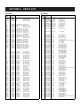
Page is loading ...
Page is loading ...
Page is loading ...
Page is loading ...
Page is loading ...
Page is loading ...
Page is loading ...
Page is loading ...
Page is loading ...
Page is loading ...
Page is loading ...
Page is loading ...
Page is loading ...
Page is loading ...
Page is loading ...
Page is loading ...
Page is loading ...
Page is loading ...
Page is loading ...
Page is loading ...
Page is loading ...
Page is loading ...
Page is loading ...
Page is loading ...
Page is loading ...
Page is loading ...
Page is loading ...
Page is loading ...
Page is loading ...
Page is loading ...
Page is loading ...
Page is loading ...
Page is loading ...
Page is loading ...
Page is loading ...
Page is loading ...
Page is loading ...
-
 1
1
-
 2
2
-
 3
3
-
 4
4
-
 5
5
-
 6
6
-
 7
7
-
 8
8
-
 9
9
-
 10
10
-
 11
11
-
 12
12
-
 13
13
-
 14
14
-
 15
15
-
 16
16
-
 17
17
-
 18
18
-
 19
19
-
 20
20
-
 21
21
-
 22
22
-
 23
23
-
 24
24
-
 25
25
-
 26
26
-
 27
27
-
 28
28
-
 29
29
-
 30
30
-
 31
31
-
 32
32
-
 33
33
-
 34
34
-
 35
35
-
 36
36
-
 37
37
-
 38
38
-
 39
39
-
 40
40
-
 41
41
-
 42
42
-
 43
43
-
 44
44
-
 45
45
-
 46
46
-
 47
47
-
 48
48
-
 49
49
-
 50
50
-
 51
51
-
 52
52
-
 53
53
-
 54
54
-
 55
55
-
 56
56
-
 57
57


Ask a question and I''ll find the answer in the document
Finding information in a document is now easier with AI
Related papers
Other documents
-
LG AX8370 Clout Hard reset manual
-
SEIKAKU TECHNICAL GROUP H38VT2001 User manual
-
-
Samsung VP-D451(i) User manual
-
 ChatterBox KA9HJC-X1 User manual
-
York DJ-1400QN User manual
-
Vertex Standard VX-2500U User manual
-
HYT TC-780 Specification
-
YAESU FT-7800R Technical Supplement
-
Kyosho IFW621/622 User manual
