Dynamic Engineering PMC-BiSerial-III HW2 User manual
- Type
- User manual

DYNAMIC ENGINEERING
150 DuBois, Suite 3 Santa Cruz, CA 95060
(831) 457-8891 Fax (831) 457-4793
www.dyneng.com
Est. 1988
User Manual
PMC-BiSerial-III HW2
32 channel
Bi-directional Manchester, SDLC and
Asynchronous Interface
PMC Module
Revision A
Corresponding Hardware: Revision C
10-2005-0503
Corresponding Firmware: Revision B

Embedded Solutions Page 2 of 50
PMC-BiSerial-III HW2
Bi-Directional Serial Data Interface
PMC Module
Dynamic Engineering
150 DuBois, Suite 3
Santa Cruz, CA 95060
(831) 457-8891
FAX: (831) 457-4793
This document contains information of
proprietary interest to Dynamic Engineering. It
has been supplied in confidence and the
recipient, by accepting this material, agrees that
the subject matter will not be copied or
reproduced, in whole or in part, nor its contents
revealed in any manner or to any person except
to meet the purpose for which it was delivered.
Dynamic Engineering has made every effort to
ensure that this manual is accurate and
complete. Still, the compan
y
reserves the ri
g
ht to
make improvements or changes in the product
described in this document at any time and
without notice. Furthermore, D
y
namic
Engineering assumes no liability arising out of
the application or use of the device described
herein.
The electronic equipment described herein
g
enerates, uses, and can radiate radio frequenc
y
energy. Operation of this equipment in a
residential area is likely to cause radio
interference, in which case the user, at his own
expense, will be required to take whatever
measures may be required to correct the
interference.
Dynamic Engineering’s products are not
authorized for use as critical components in life
support devices or systems without the express
written approval of the president of Dynamic
Engineering.
This product has been designed to operate with
PMC Module carriers and compatible user-
provided equipment. Connection of incompatible
hardware is likely to cause serious damage.
©2005-2007 by Dynamic Engineering.
Other trademarks and registered trademarks are
owned by their respective manufactures.
Revised September 25, 2007.

Embedded Solutions Page 3 of 50
Table of Contents
PRODUCT DESCRIPTION 6
THEORY OF OPERATION 11
ADDRESS MAP 14
PROGRAMMING 16
REGISTER DEFINITIONS 17
BIS3_BASE 17
BIS3_ID 18
BIS3_START_SET 18
BIS3_START_RDBK 18
BIS3_START_CLR 19
BIS3_IO_DATA 20
BIS3_IO_DIR 20
BIS3_IO_TERM 21
BIS3_IO_MUX 21
BIS3_IO_UCNTL 22
BIS3_IO_RDBK 22
BIS3_IO_RDBKUPR 23
BIS3_STAT_FIFO 23
BIS3_PLL_CMD, PLL_RDBK 24
BIS3_SM_CNTL7-0 25
BIS3_SDLC_CNTL5-0 28
BIS3_ASYNC_CNTL11-0 30
BIS3_CHAN_MODE 32
BIS3_INT_STAT 33
BIS3_I2OAR 33
BIS3_SM_MEM31-0 34
Mode Resource Mapping 39
Interrupts 40
Loop-back 41
PMC PCI PN1 INTERFACE PIN ASSIGNMENT 42
PMC PCI PN2 INTERFACE PIN ASSIGNMENT 43

Embedded Solutions Page 4 of 50
BISERIAL III FRONT PANEL I/O PIN ASSIGNMENT 44
APPLICATIONS GUIDE 45
Interfacing 45
CONSTRUCTION AND RELIABILITY 46
THERMAL CONSIDERATIONS 46
WARRANTY AND REPAIR 47
SERVICE POLICY 47
OUT OF WARRANTY REPAIRS 47
FOR SERVICE CONTACT: 47
SPECIFICATIONS 48
ORDER INFORMATION 50
SCHEMATICS 50

Embedded Solutions Page 5 of 50
List of Figures
FIGURE 1
PMC BISERIAL-III BASE BLOCK DIAGRAM 6
FIGURE 2 PMC BISERIAL-III-HW2 P2P BLOCK DIAGRAM 7
FIGURE 3 PMC BISERIAL-III-HW2 SDLC BLOCK DIAGRAM 8
FIGURE 4 PMC BISERIAL-III-HW2 ASYNC BLOCK DIAGRAM 9
FIGURE 5 PMC BISERIAL III HW2 MANCHESTER TIMING DIAGRAM 12
FIGURE 6 PMC BISERIAL-II I-HW2 INTERNAL ADDRESS MAP 15
FIGURE 7 PMC BISERIAL-III BASE CONTROL REGISTER BIT MAP 17
FIGURE 8 PMC BISERIAL-III DESIGN ID REGISTER BIT MAP 18
FIGURE 9 PMC BISERIAL-III START SET REGISTER 18
FIGURE 10 PMC BISERIAL-III START CLEAR REGISTER 19
FIGURE 11 PMC BISERIAL-III PARALLEL OUTPUT DATA BIT MAP 20
FIGURE 12 PMC BISERIAL-III DIRECTION CONTROL PORT 20
FIGURE 13 PMC BISERIAL-III TERMINATION CONTROL PORT 21
FIGURE 14 PMC BISERIAL-III MUX CONTROL PORT 21
FIGURE 15 PMC BISERIAL-III UPPER CONTROL PORT 22
FIGURE 16 PMC BISERIAL-III I/O READBACK PORT 22
FIGURE 17 PMC BISERIAL-III I/O READBACK PORT 23
FIGURE 18 PMC BISERIAL-III SWITCH PORT 23
FIGURE 19 PMC BISERIAL-III PLL CONTROL 24
FIGURE 20 PMC BISERIAL-III STATE MACHINE CONTROL REGISTERS 25
FIGURE 21 PMC BISERIAL-III SDLC CONTROL REGISTERS 28
FIGURE 22 PMC BISERIAL-III SDLC CONTROL REGISTERS 30
FIGURE 23 PMC BISERIAL-III CHANNEL MODE CONTROL REGISTER 32
FIGURE 24 PMC BISERIAL-III INTERRUPT STATUS REGISTER 33
FIGURE 25 PMC BISERIAL-III I2O ADDRESS REGISTER 33
FIGURE 26 PMC BISERIAL-III PN1 INTERFACE 42
FIGURE 27 PMC BISERIAL-III PN2 INTERFACE 43
FIGURE 28 PMC BISERIAL-III FRONT PANEL INTERFACE 44

Embedded Solutions Page 6 of 50
Product Description
The PMC BiSerial-III-HW2 is part of the PMC Module family of modular I/O components
by Dynamic Engineering. The PMC BiSerial-III is capable of providing multiple serial
protocols. The HW2 protocol implemented provides 8 Manchester encoded inputs and
outputs and 6 additional blocks that can each be configured as either one full-duplex
SDLC I/O or two full-duplex asynchronous (UART) I/O.
Other custom interfaces are available. We will redesign the state machines and create
a custom interface protocol. That protocol will then be offered as a “standard” special
order product. Please see our web page for current protocols offered. Please contact
Dynamic Engineering with your custom application.
485/LVDS buffers
termination
PCI IF
FIFO B
128K x 32
FIFO A
128K x 32
State
Machine
B
State
Machine
A
Data Flow
Control
PLL
FIGURE 1 PMC BISERIAL-III BASE BLOCK DIAGRAM

Embedded Solutions Page 7 of 50
The standard configuration shown in Figure 1 makes use of two external (to the Xilinx)
FIFOs. The FIFOs can be as large as 128K deep x 32 bits wide. Some designs do not
require so much memory, and are more efficiently implemented using the Xilinx internal
memory.
FIGURE 2 PMC BISERIAL-III-HW2 P2P BLOCK DIAGRAM
The HW2 implementation has 32 – Dual Port RAM (DPR) blocks implemented using
the Xilinx internal block RAM. Each channel has one or more associated DPRs
depending on which mode is active. Each DPR is configured to have a 32-bit port on
the PCI side, and a 16-bit port on the I/O side.
The lower eight channels are configured with the point-to-point interface that was used
on the HW1. In this mode when operating in the bidirectional mode the DPR is split in
half to provide both transmit, and receive buffers. In the unidirectional mode the full
DPR can be used for transmit or receive data.

Embedded Solutions Page 8 of 50
The data rates are programmable to either 400 KHz or 5 MHz. Usually the 5 MHz rate
is used in the unidirectional mode and the 400 KHz in the bidirectional mode. The data
is Manchester encoded. The hardware uses a higher rate clock to separate the clock
and data embedded within the Manchester data stream.
The remaining 24 channels are divided into six four-channel blocks that can each be
configured as either one full-duplex SDLC interface or two full-duplex asynchronous
interfaces.
The SDLC interface uses programmable PLL clock A as its reference frequency with
clock and data in and out comprising the four I/O lines of the channel block. The four
DPRs are partitioned into two blocks each for transmit and receive circular buffers that
have independently specified start and stop addresses and separate transmit and
receive interrupts.
FIGURE 3 PMC BISERIAL-III-HW2 SDLC BLOCK DIAGRAM

Embedded Solutions Page 9 of 50
Each asynchronous interface uses either programmable PLL clock B or a fixed 5 MHz
as its 16x reference frequency with data in and out using two of the four I/O lines of the
channel block. Two DPRs are used for each asynchronous interface, one each for
transmit and receive circular buffers that have independently specified start and stop
addresses.
FIGURE 4 PMC BISERIAL-III-HW2 ASYNC BLOCK DIAGRAM
The two asynchronous interfaces in a channel block are independently configurable
and each have separate receive and transmit interrupts.
All the data I/O lines on the HW2 are programmable to be register controlled or state-
machine controlled. Any or all of the bits can be used as a parallel port instead of being
dedicated to a specific I/O protocol. Thirty-four differential I/O are provided at the front
bezel (32 of the 34 at Pn4) for the serial signals. The drivers and receivers conform to
the RS-485 specification (exceeds RS-422 specification). The RS-485 input signals are
selectively terminated with 100Ω. The termination resistors are in two-element

Embedded Solutions Page 10 of 50
packages to allow flexible termination options for custom formats and protocols.
Optional pullup/pulldown resistor packs can also be installed to provide a logic ‘1’ on
undriven lines. The terminations and transceivers are programmable through the Xilinx
device to provide the proper mix of outputs and inputs and terminations needed for a
specific protocol implementation. The terminations are programmable for all I/O.
All configuration registers support read and write operations for maximum software
convenience, and all addresses are long word aligned.
The PMC BiSerial-III conforms to the PMC and CMC draft standards. This guarantees
compatibility with multiple PMC Carrier boards. Because the PMC may be mounted on
different form factors, while maintaining plug and software compatibility, system
prototyping may be done on one PMC Carrier board, with final system implementation
uses a different one.
The PMC BiSerial-III uses a 10 mm inter-board spacing for the front panel, standoffs,
and PMC connectors. The 10 mm height is the "standard" height and will work in most
systems with most carriers. If your carrier has non-standard connectors (height) to
mate with the PMC BiSerial-III, please let us know. We may be able to do a special
build with a different height connector to compensate.
Interrupts are supported by the PMC BiSerial-III-HW2. An interrupt can be configured to
occur at the end of a transmitted packet or message. An interrupt will be set at the end
of a received packet or message. All interrupts are individually maskable, and a master
interrupt enable is also provided to disable all interrupts simultaneously. The current
status is available for the state-machines making it possible to operate in a polled
mode. I2O interrupt processing is also available.

Embedded Solutions Page 11 of 50
Theory of Operation
The PMC BiSerial-III-HW2 is designed for transferring data from one point to another
with three simple serial protocols.
The PMC BiSerial-III-HW2 features a Xilinx FPGA. The FPGA contains all of the
registers and protocol controlling elements of the BiSerial III design. Only the PLL,
transceivers, and switches are external to the Xilinx device.
The PMC BiSerial-III is a part of the PMC Module family of modular I/O products. It
meets the PMC and CMC draft Standards. In standard configuration, the PMC
BiSerial-III is a Type 1 mechanical with only low-profile components on the back of the
board and one slot wide, with 10 mm inter-board height. Contact Dynamic Engineering
for a copy of this specification. It is assumed that the reader is at least casually familiar
with this document and basic logic design.
The PCI interface to the host CPU is controlled by a logic block within the Xilinx. The
BiSerial III design requires one wait state for read or write cycles to any address. The
PMC BiSerial-III is capable of supporting 40 MBytes per second into and out of the
DPR. With a Windows® read/write loop better than 20 MB/sec is attained on most
computers. The wait states refer to the number of clocks after the PCI core decode
before the “terminate with data” state is reached. Two additional clock periods account
for the 1 clock delay to decode the signals from the PCI bus and to convert the
terminate with data state into the TRDY signal.
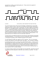
The BiSerial III can support many protocols. The PMC BiSerial-III-HW2 uses
Manchester serial encoded data and clock for its point-to-point interface. Data is sent
in 16-bit words; concatenated for multiple word transfers. The Manchester timing is
shown in the next diagram.
State machines within the FPGA control all transfers to and from the internal RAM and
I/O logic. The TX state machine reads from the transmit memory and loads the shift
registers before sending the data. The RX state machine receives data from the data
buffers and takes care of moving data from the shift register into the RX memory.
Data is read from the TX memory. The first two locations are control words. The
control words are stored for state-machine use. The first data word is then read and
loaded into the output shift register and the CRC generator. The Shift register is
enabled to shift the data out. As the bits are shifted out of the shift register the data is
encoded for Manchester compatibility. When the last data word has been loaded into
the CRC and shift register, the hardware completes the CRC processing to be prepared
for the last load to the shift register. Once the CRC has been transmitted the hardware
checks to see if more data is to be sent or if this was the last packet in the message.
There are several options including using a software CRC instead of the hardware

Embedded Solutions Page 12 of 50
generated one, adding a post amble pattern etc. Please refer to the register bit
definitions for more details.
DATA IN/OUT
0
10
0
011
0
11 0
10
MANCHESTER ENCODING
FIGURE 5 PMC BISERIAL III HW2 MANCHESTER TIMING DIAGRAM
The receive function uses a free running shift register coupled with the receive state-
machine to capture the data. When the receiver detects the idle pattern followed by 4
Manchester ‘0’s the receiver starts to capture data. The data is read in and stored into
the DPR. The embedded length is used to determine where the CRC should be. The
CRC is calculated as the data is received and checked against the CRC received with
the packet. An error bit is set if the two do not match. Manchester errors within the
packet are detected, and used to abort processing of the message. After a packet has
been received the Post Amble is tested to see that it follows the proper protocol. The
Manchester and Post Amble errors are also latched in status bits.
This document is somewhat restricted as to the technical content allowed in describing
the electrical interface. The document “Point-to-Point Data Bus Protocol Specification –
C72-1199-069” provides a more complete description of the interface.
The PMC BiSerial-III-HW2 also supports an SDLC interface. This is a synchronous
interface with separate clock and data inputs and outputs. Each message is delimited
by start/stop flag characters consisting of an eight-bit (0x7E) pattern. In order to avoid
false flag detection from the data pattern, if five consecutive ones appear anywhere in
the data stream, an additional zero is inserted to avoid having six consecutive one bits.
On the receive side, when five ones are received the sixth bit is monitored. If it is a
zero, it is removed from the data stream, if it is a one then either a start/stop flag or an
abort character (0xFE) has been detected.
To send a message, write the message data to the transmit DPRs, specify the start and
stop addresses and configuration control bits, then enable the transmitter. The state-

Embedded Solutions Page 13 of 50
machine will load the start address, send the opening flag character and begin sending
data sequentially LSB first until the end address is reached and the closing flag is sent.
If the TX clear is enabled, the transmitter will be automatically disabled when the
transmission is complete. Otherwise, the transmitter will wait, pointing at the next
address after the end address. If additional data has been or is later written to the
DPR, a new message can be started by entering a new end address. The transmit
state-machine will then start a new message and continue sending data until the new
end address has been reached. If the end of the second DPR block is reached before
the end address, the transmitter will proceed to the beginning of the first DPR block and
continue until the end address is reached. Likewise when the end of the first DPR is
reached, the transmitter continues with the beginning of the second DPR.
To receive a message the receiver must be enabled, but only the starting address of
the receive buffer needs to be specified. Data will be stored sequentially starting at that
address until the closing flag is detected. This will latch an RX interrupt status and can
cause an interrupt if enabled. The last address that data (16-bit words) is stored in is
latched and can be read from the control register as a read-only field.
The transmit interrupt is mapped to the first interrupt line of the channel block and the
receive interrupt is mapped to the second interrupt line. The remaining two interrupt
lines are not used in SDLC mode.
An asynchronous interface is also available on the PMC BiSerial-III-HW2. This protocol
uses one start-bit (low) eight data-bits no parity and one stop-bit (high). The marking
(idle) state of the line is high and eleven bit-periods of this high state will be interpreted
as the end-of-message condition.
The clock reference is supplied by either PLL clock B or 5 MHz derived from the on-
board oscillator. This frequency is sixteen times the bit rate of the interface. The
transmit clock is derived by a straight divide-by sixteen circuit, while the receive state-
machine uses the higher frequency to detect data bits and will re-sync its clock counter
when detected data transitions are close but not exactly on sixteen clock boundaries.
This allows for greater flexibility in matching transmitter and receiver clock frequencies.
Each asynchronous interface uses two DPR blocks, one for the transmitter and one for
the receiver. The process of sending and receiving messages is similar to the SDLC
interface except that only half as much memory is available for the receive and transmit
buffers. Also the receiver end address that is latched when a received message
completes is a byte address. That is the lower two bits of the address specify which
byte was the last to be written, while the remaining address bits specify the 32-bit word
that contains that byte e.g. an end address of 0x3ff would indicate that all four bytes of
the 255
th
word of the receive DPR were written.
The transmit interrupt is mapped to the first or third interrupt line of the channel block
and the receive interrupt is mapped to the second or fourth interrupt line.

Embedded Solutions Page 14 of 50
Address Map
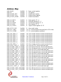
BIS3_BASE 0x0000 0 Base control register
BIS3_ID 0x0004 1 ID register
BIS3_START_SET 0x0008 2 Start-bit set register
BIS3_START_CLR 0x000C 3 Start-bit clear register
BIS3_START_RDBK 0x0008 2 Start-bit read-back
BIS3_IO_DATA 0x0010 4 Data register 31 - 0
BIS3_IO_DIR 0x0014 5 Direction register 31 - 0
BIS3_IO_TERM 0x0018 6 Termination register 31 - 0
BIS3_IO_MUX 0x001C 6 Mux register 31 - 0
BIS3_IO_UCNTL 0x0020 8 Upper control register 33, 32
BIS3_STAT_FIFO 0x0024 9 User switch value
BIS3_PLL_CMD 0x0028 10 PLL control register and read-back of PLL data
BIS3_PLL_RDBK 0x002C 11 PLL control register read-back
BIS3_SM_CNTL_0 0x0040 16 Chan 0 state-machine control read-write port
BIS3_SM_CNTL_1 0x0044 17 Chan 1 state-machine control read-write port
BIS3_SM_CNTL_2 0x0048 18 Chan 2 state-machine control read-write port
BIS3_SM_CNTL_3 0x004C 19 Chan 3 state-machine control read-write port
BIS3_SM_CNTL_4 0x0050 20 Chan 4 state-machine control read-write port
BIS3_SM_CNTL_5 0x0054 21 Chan 5 state-machine control read-write port
BIS3_SM_CNTL_6 0x0058 22 Chan 6 state-machine control read-write port
BIS3_SM_CNTL_7 0x005C 23 Chan 7 state-machine control read-write port
BIS3_SDLC_CNTL_0 0x0060 24 Chan 8 SDLC control read-write port
BIS3_ASYNC_CNTL_0 0x0060 24 Chan 8 asynchronous control read-write port
BIS3_ASYNC_CNTL_1 0x0068 26 Chan 10 asynchronous control read-write port
BIS3_SDLC_CNTL_1 0x0060 28 Chan 12 SDLC control read-write port
BIS3_ASYNC_CNTL_2 0x0060 28 Chan 12 asynchronous control read-write port
BIS3_ASYNC_CNTL_3 0x0068 30 Chan 14 asynchronous control read-write port
BIS3_SDLC_CNTL_2 0x0070 32 Chan 16 SDLC control read-write port
BIS3_ASYNC_CNTL_4 0x0070 32 Chan 16 asynchronous control read-write port
BIS3_ASYNC_CNTL_5 0x0078 34 Chan 18 asynchronous control read-write port
BIS3_SDLC_CNTL_3 0x0080 36 Chan 20 SDLC control read-write port
BIS3_ASYNC_CNTL_6 0x0080 36 Chan 20 asynchronous control read-write port
BIS3_ASYNC_CNTL_7 0x0088 38 Chan 22 asynchronous control read-write port
BIS3_SDLC_CNTL_4 0x00A0 40 Chan 24 SDLC control read-write port
BIS3_ASYNC_CNTL_8 0x00A0 40 Chan 24 asynchronous control read-write port
BIS3_ASYNC_CNTL_9 0x00A8 42 Chan 26 asynchronous control read-write port
BIS3_SDLC_CNTL_5 0x00B0 44 Chan 28 SDLC control read-write port
BIS3_ASYNC_CNTL_10 0x00B0 44 Chan 28 asynchronous control read-write port
BIS3_ASYNC_CNTL_11 0x00B8 46 Chan 30 asynchronous control read-write port

Embedded Solutions Page 15 of 50
BIS3_IO_RDBK 0x00C0 48 External I/O read register
BIS3_IO_RDBKUPR 0x00C4 49 External I/O upper bits read register
BIS3_CHAN_MODE 0x00C8 50 Channel mode control register
BIS3_INT_STAT 0x00CC 51 Interrupt status and clear register
BIS3_I2OAR 0x00D4 53 I2O address storage register
BIS3_SM_MEM_0 0x00800 Dual-port RAM 0 read/write port
BIS3_SM_MEM_1 0x01000 Dual-port RAM 1 read/write port
BIS3_SM_MEM_2 0x01800 Dual-port RAM 2 read/write port
BIS3_SM_MEM_3 0x02000 Dual-port RAM 3 read/write port
BIS3_SM_MEM_4 0x02800 Dual-port RAM 4 read/write port
BIS3_SM_MEM_5 0x03000 Dual-port RAM 5 read/write port
BIS3_SM_MEM_6 0x03800 Dual-port RAM 6 read/write port
BIS3_SM_MEM_7 0x04000 Dual-port RAM 7 read/write port
BIS3_SM_MEM_8 0x04800 Dual-port RAM 8 read/write port
BIS3_SM_MEM_9 0x05000 Dual-port RAM 9 read/write port
BIS3_SM_MEM_10 0x05800 Dual-port RAM 10read/write port
BIS3_SM_MEM_11 0x06000 Dual-port RAM 11 read/write port
BIS3_SM_MEM_12 0x06800 Dual-port RAM 12 read/write port
BIS3_SM_MEM_13 0x07000 Dual-port RAM 13 read/write port
BIS3_SM_MEM_14 0x07800 Dual-port RAM 14 read/write port
BIS3_SM_MEM_15 0x08000 Dual-port RAM 15 read/write port
BIS3_SM_MEM_16 0x08800 Dual-port RAM 16 read/write port
BIS3_SM_MEM_17 0x09000 Dual-port RAM 17 read/write port
BIS3_SM_MEM_18 0x09800 Dual-port RAM 18 read/write port
BIS3_SM_MEM_19 0x0A000 Dual-port RAM 19 read/write port
BIS3_SM_MEM_20 0x0A800 Dual-port RAM 20 read/write port
BIS3_SM_MEM_21 0x0B000 Dual-port RAM 21 read/write port
BIS3_SM_MEM_22 0x0B800 Dual-port RAM 22 read/write port
BIS3_SM_MEM_23 0x0C000 Dual-port RAM 23 read/write port
BIS3_SM_MEM_24 0x0C800 Dual-port RAM 24 read/write port
BIS3_SM_MEM_25 0x0D000 Dual-port RAM 25 read/write port
BIS3_SM_MEM_26 0x0D800 Dual-port RAM 26 read/write port
BIS3_SM_MEM_27 0x0E000 Dual-port RAM 27 read/write port
BIS3_SM_MEM_28 0x0E800 Dual-port RAM 28 read/write port
BIS3_SM_MEM_29 0x0F000 Dual-port RAM 29 read/write port
BIS3_SM_MEM_30 0x0F800 Dual-port RAM 30 read/write port
BIS3_SM_MEM_31 0x10000 Dual-port RAM 31 read/write port
FIGURE 6 PMC BISERIAL-II
I-HW2 INTERNAL ADDRESS MAP
The address map provided is for the local decoding performed within the PMC BiSerial-
III. The addresses are all offsets from a base address, which is assigned by the system
when the PCI bus is configured.

Embedded Solutions Page 16 of 50
Programming
Programming the PMC BiSerial-III-HW2 requires only the ability to read and write data
from the host. The base address of the module refers to the first user address for the
slot in which the PMC is installed. This address is determined during system
configuration of the PCI bus.
Depending on the software environment it may be necessary to set-up the system
software with the PMC BiSerial-III "registration" data. For example in WindowsNT there
is a system registry, which is used to identify the resident hardware.
In order to receive data the software is only required to enable the Rx channel and set
the frequency parameters. To transmit the software will need to load the message into
the appropriate Dual Port RAM, set the frequency and mode and enable the transmitter.
The interrupt service routine should be loaded and the interrupt mask set. The interrupt
service routine can be configured to respond to the channel interrupts on an individual
basis. After the interrupt is received, the data can be retrieved. An efficient loop can
then be implemented to fetch the data. New messages can be received even as the
current one is read from the Dual Port RAM.
The TX interrupt indicates to the software that a message has been sent and that the
message has completed. If more than one interrupt is enabled, then the interrupt
service routine (ISR) needs to read the status to see which source caused the interrupt.
The status bits are latched, and are explicitly cleared by writing a one to the
corresponding bit. It is a good idea to read the status register and write that value back
to clear all the latched interrupt status bits before starting a transfer. This will insure
that the interrupt status values read by the ISR came from the current transfer.
Refer to the Theory of Operation section above and the Interrupts section below for
more information regarding the exact sequencing and interrupt definitions.
The VendorId = 0x10EE. The CardId = 0x002E.
Flash design ID = 0x0002, Current Flash revision = 0x0002

Embedded Solutions Page 17 of 50
Register Definitions
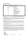
BIS3_BASE
[$00] BiSerial III Base Control Register Port read/write
Base Control Register
DATA BIT DESCRIPTION
31-4 Spare
3 I2O CLR
2 I2O EN
1 Interrupt Set
0 Interrupt Enable Master
FIGURE 7 PMC BISERIAL-III BASE CONTROL REGISTER BIT MAP
All bits are active high and are reset on power-up or reset command.
Interrupt Enable Master : When '1' allows interrupts generated by the
PMC-BiSerial-III-HW2 to be driven onto the carrier (INTA). When '0' the interrupts can
be individually enabled and used for status without driving the backplane. Polled
operation can be performed in this mode.
Interrupt Set : When '1' and the Master is enabled, this bit forces an interrupt request.
This feature is useful for testing and software development.
I2O EN : When ‘1’ allows the I2O interrupts to be activated. Interrupt requests are
routed to the address stored in the I2O Address Register (I2OAR). When ‘0’ the I2O
function is disabled.
I2O CLR : When ‘1’ this bit will cause the current data stored in the I2O collection
register to be cleared. It is recommended that this register clear bit be used
immediately before enabling I2O operation to prevent previously stored events from
causing interrupts.

Embedded Solutions Page 18 of 50
BIS3_ID
[$04] BiSerial III FLASH status/Driver Status Port read only
Design Number / FLASH Revision
DATA BIT DESCRIPTION
31-16 Design/Driver ID
15-0 FLASH revision
FIGURE 8 PMC BISERIAL-III DESIGN ID REGISTER BIT MAP
The Design / Driver ID for the HW2 project is 0x0002. The FLASH ID will be updated
as features are added or revisions made. See the programming section for the current
FLASH revision.
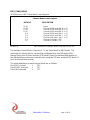
BIS3_START_SET
BIS3_START_RDBK
[$08] BiSerial III Start Set Control Register Port read/write
Start Set Register
DATA BIT DESCRIPTION
7-0 Channels to activate (write only)
7-0 Channels that are active (read only)
FIGURE 9 PMC BISERIAL-III START SET REGISTER
To start a channel, write a ‘1’ to the corresponding bit. To clear a channel use the Start
Clear register. Read back from this port reflects the channels which are active. Please
note that channel these bits can be cleared by the channel state-machines.

Embedded Solutions Page 19 of 50
BIS3_START_CLR
[$0C] BiSerial III Start Clear Control Register Port write only
Start Clear Register
DATA BIT DESCRIPTION
7-0 Clear the active Start Bits
FIGURE 10 PMC BISERIAL-III START CLEAR REGISTER
Writing a ‘1’ to a channel clear bit will cause that channels Start Bit to be cleared. The
Channel will complete the current operation and then abort processing. Reading from
the RDBK register will show the active channels. The state-machine may be running at
a significantly slower rate than the PCI bus. There may be some delay in sensing that
the start abort has been set for a particular channel.
The delay can be estimated to be the period of the clock in use and 12 periods. For
transmit the clock rate is 2x the data rate. For receive the clock rate is 8x the data rate.
At low speed in transmit mode the delay would be 12x (1/800 Khz) => 15 uS or so.
These are worst case delays.
Please note that the “ready_busy” bit can be used to check when an aborted channel is
ready for a new start command. Please refer to the channel control registers.

Embedded Solutions Page 20 of 50
BIS3_IO_DATA
[$10] BiSerial III Parallel Data Output Register read/write
Parallel Data Output Register
DATA BIT DESCRIPTION
31-0 parallel output data
FIGURE 11 PMC BISERIAL-III PARALLEL OUTPUT DATA BIT MAP
There are 32 potential output bits in the parallel port. The Direction, Termination, and
Mux Control registers are also involved. When the direction is set to output, and the
Mux control set to parallel port the bit definitions from this register are driven onto the
corresponding parallel port lines.
This port is direct read-write of the register. The I/O side is read-back from the
BIS3_IO_RDBK port. It is possible that the output data does not match the I/O data in
the case of the Direction bits being set to input or the Mux control set to state-machine.
BIS3_IO_DIR
[$14] BiSerial III Direction Port read/write
Direction Control Port
DATA BIT DESCRIPTION
31-0 Parallel Port Direction Control bits
FIGURE 12 PMC BISERIAL-III DIRECTION CONTROL PORT
When set (‘1’) the corresponding bit in the parallel port is a transmitter. When cleared
(‘0’) the corresponding bit is a receiver. The corresponding Mux control bits must also
be configured for parallel port.
Page is loading ...
Page is loading ...
Page is loading ...
Page is loading ...
Page is loading ...
Page is loading ...
Page is loading ...
Page is loading ...
Page is loading ...
Page is loading ...
Page is loading ...
Page is loading ...
Page is loading ...
Page is loading ...
Page is loading ...
Page is loading ...
Page is loading ...
Page is loading ...
Page is loading ...
Page is loading ...
Page is loading ...
Page is loading ...
Page is loading ...
Page is loading ...
Page is loading ...
Page is loading ...
Page is loading ...
Page is loading ...
Page is loading ...
Page is loading ...
-
 1
1
-
 2
2
-
 3
3
-
 4
4
-
 5
5
-
 6
6
-
 7
7
-
 8
8
-
 9
9
-
 10
10
-
 11
11
-
 12
12
-
 13
13
-
 14
14
-
 15
15
-
 16
16
-
 17
17
-
 18
18
-
 19
19
-
 20
20
-
 21
21
-
 22
22
-
 23
23
-
 24
24
-
 25
25
-
 26
26
-
 27
27
-
 28
28
-
 29
29
-
 30
30
-
 31
31
-
 32
32
-
 33
33
-
 34
34
-
 35
35
-
 36
36
-
 37
37
-
 38
38
-
 39
39
-
 40
40
-
 41
41
-
 42
42
-
 43
43
-
 44
44
-
 45
45
-
 46
46
-
 47
47
-
 48
48
-
 49
49
-
 50
50


