
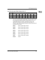
MVME172
VME Embedded Controller
Programmer’s
Reference Guide
VME172A/PG2
Edition of February 1999

Notice
While reasonable efforts have been made to assure the accuracy of this document,
Motorola, Inc. assumes no liability resulting from any omissions in this document, or from
the use of the information obtained therein. Motorola reserves the right to revise this
document and to make changes from time to time in the content hereof without obligation
of Motorola to notify any person of such revision or changes.
No part of this material may be reproduced or copied in any tangible medium, or stored in
a retrieval system, or transmitted in any form, or by any means, radio, electronic,
mechanical, photocopying, recording or facsimile, or otherwise, without the prior written
permission of Motorola, Inc.
It is possible that this publication may contain reference to, or information about Motorola
products (machines and programs), programming, or services that are not announced in
your country. Such references or information must not be construed to mean that Motorola
intends to announce such Motorola products, programming, or services in your country.
Restricted Rights Legend
If the documentation contained herein is supplied, directly or indirectly, to the U.S.
Government, the following notice shall apply unless otherwise agreed to in writing by
Motorola, Inc.
Use, duplication, or disclosure by the Government is subject to restrictions as set forth in
subparagraph (c)(1)(ii) of the Rights in Technical Data and Computer Software clause at
DFARS 252.227-7013.
Motorola, Inc.
Computer Group
2900 South Diablo Way
Tempe, Arizona 85282

Preface
This manual provides board level information and detailed ASIC chip information
including register bit descriptions for the MVME172 Embedded Controller. The
information contained in this manual applies to the following MVME172 models:
This manual is intended for anyone who wants to program these boards in order to design
OEM systems, supply additional capability to an existing compatible system, or work in a
lab environment for experimental purposes.
A basic knowledge of computers and digital logic is assumed.
To use this manual, you should be familiar with the publications listed in Related
Documentation below.
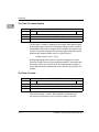
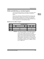
Manual Terminology
Throughout this manual, a convention is used which precedes data and address parameters
by a character identifying the numeric format as follows:
For example, “12” is the decimal number twelve, and “$12” is the decimal number
eighteen.
Unless otherwise specified, all address references are in hexadecimal.
An asterisk (*) following the signal name for signals which are level significant denotes that
the signal is true or valid when the signal is low.
An asterisk (*) following the signal name for signals which are edge significant denotes that
the actions initiated by that signal occur on high to low transition.
MVME172-303
MVME172-213 MVME172-313 MVME172-413 MVME172-513
MVME172-223 MVME172-323
MVME172-233 MVME172-333 MVME172-433
MVME172-243 MVME172-343
MVME172-253 MVME172-353 MVME172-453
MVME172-263 MVME172-363
MVME172-373
$ dollar specifies a hexadecimal character
% percent specifies a binary number
& ampersand specifies a decimal number

In this manual, assertion and negation are used to specify forcing a signal to a particular
state. In particular, assertion and assert refer to a signal that is active or true; negation and
negate indicate a signal that is inactive or false. These terms are used independently of the
voltage level (high or low) that they represent.
Data and address sizes are defined as follows:
❏ A byte is eight bits, numbered 0 through 7, with bit 0 being the least significant.
❏ A word is 16 bits, numbered 0 through 15, with bit 0 being the least significant.
❏ A longword is 32 bits, numbered 0 through 31, with bit 0 being the least
significant.
The terms control bit, status bit, true, and false are used extensively in this document. The
term control bit is used to describe a bit in a register that can be set and cleared under
software control. The term true is used to indicate that a bit is in the state that enables the
function it controls. The term false is used to indicate that the bit is in the state that disables
the function it controls. In all tables, the terms 0 and 1 are used to describe the actual value
that should be written to the bit, or the value that it yields when read. The term status bit is
used to describe a bit in a register that reflects a specific condition. The status bit can be
read by software to determine operational or exception conditions.
Recent Updates
This edition of the MVME172 VME Embedded Controller Programmer’s Reference Guide
incorporates the following changes:
❏ The ‘‘MVME172 Version Register‘‘ section has an improved description of the
function of bit V6.
❏ The ‘‘PROM Access Time Control Register’’ and ‘‘Flash Access Time Control
Register’’ have clarification relating to bus speeds and access times with the
MVME172’s MC68060 processor.
❏ In accordance with recent MCG practice, the ‘‘Related Documentation’’ section
has been moved from the front of the document to a separate appendix.

The computer programs stored in the Read Only Memory of this device contain material
copyrighted by Motorola Inc., first published 1990, and may be used only under a license
such as the License for Computer Programs (Article 14) contained in Motorola’s Terms and
Conditions of Sale, Rev. 1/79.
!
WARNING
This equipment generates, uses, and can radiate electro- magnetic
energy. It may cause or be susceptible to electro-magnetic
interference (EMI) if not installed and used in a cabinet with
adequate EMI protection.
Motorola and the Motorola symbol are registered trademarks of Motorola, Inc.
All other products mentioned in this document are trademarks or registered trademarks of
their respective holders.
© Copyright Motorola, Inc. 1999
All Rights Reserved
Printed in the United States of America
February 1999

Place holder

vii
Contents
CHAPTER 1 Board Description and Memory Maps
Introduction................................................................................................................1-1
Overview....................................................................................................................1-1
Requirements .............................................................................................................1-4
Block Diagrams .........................................................................................................1-5
Functional Description...............................................................................................1-5
No-VMEbus-Interface Option............................................................................1-5
VMEbus Interface and VMEchip2.....................................................................1-9
Memory Maps............................................................................................................1-9
Local Bus Memory Map.....................................................................................1-9
Normal Address Range................................................................................1-9
Detailed I/O Memory Maps.......................................................................1-21
BBRAM/TOD Clock Memory Map..........................................................1-40
Interrupt Acknowledge Map......................................................................1-46
VMEbus Memory Map.....................................................................................1-46
VMEbus Accesses to the Local Bus..........................................................1-47
VMEbus Short I/O Memory Map..............................................................1-47
Software Support Considerations ............................................................................1-47
Interrupts...........................................................................................................1-47
Cache Coherency..............................................................................................1-48
Sources of Local BERR*..................................................................................1-48
Local Bus Time-out...................................................................................1-48
VMEbus Access Time-out.........................................................................1-49
VMEbus BERR* .......................................................................................1-49
Local DRAM Parity Error.........................................................................1-49
VMEchip2 .................................................................................................1-49
Bus Error Processing.................................................................................1-49
Description of Error Conditions on the MVME172.........................................1-50
MPU Parity Error.......................................................................................1-50
MPU Off-board Error................................................................................1-51
MPU TEA - Cause Unidentified ...............................................................1-51
MPU Local Bus Time-out.........................................................................1-51
DMAC VMEbus Error ..............................................................................1-52
DMAC Parity Error...................................................................................1-52
DMAC Off-board Error.............................................................................1-53
DMAC LTO Error.....................................................................................1-53

viii
DMAC TEA - Cause Unidentified............................................................1-54
LAN Parity Error.......................................................................................1-54
LAN Off-Board Error ...............................................................................1-55
LAN LTO Error ........................................................................................1-55
SCSI Parity Error ......................................................................................1-56
SCSI Off-Board Error ...............................................................................1-56
SCSI LTO Error........................................................................................1-56
Example of the Proper Use of Bus Timers.......................................................1-57
MVME172 MC68060 Indivisible Cycles ........................................................1-58
Illegal Access to IP Modules from External VMEbus Masters .......................1-59
CHAPTER 2 VMEchip2
Introduction ...............................................................................................................2-1
Summary of Major Features...............................................................................2-1
Functional Blocks......................................................................................................2-4
Local Bus to VMEbus Interface.........................................................................2-4
Local Bus to VMEbus Requester................................................................2-7
VMEbus to Local Bus Interface.........................................................................2-9
Local Bus to VMEbus DMA Controller ..........................................................2-10
No Address Increment DMA Transfers....................................................2-12
DMAC VMEbus Requester ......................................................................2-13
Tick and Watchdog Timers...............................................................................2-14
Prescaler....................................................................................................2-14
Tick Timers...............................................................................................2-15
Watchdog Timer........................................................................................2-15
VMEbus Interrupter .........................................................................................2-16
VMEbus System Controller .............................................................................2-17
Arbiter.......................................................................................................2-17
IACK Daisy-Chain Driver ........................................................................2-17
Bus Timer..................................................................................................2-17
Reset Driver ..............................................................................................2-18
Local Bus Interrupter and Interrupt Handler....................................................2-18
Global Control and Status Registers ................................................................2-20
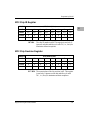
LCSR Programming Model.....................................................................................2-20
Programming the VMEbus Slave Map Decoders ............................................2-26
VMEbus Slave Ending Address Register 1 .............................................2-28
VMEbus Slave Starting Address Register 1 ............................................2-28
VMEbus Slave Ending Address Register 2 .............................................2-29
VMEbus Slave Starting Address Register 2 ............................................2-29
VMEbus Slave Address Translation Address Offset Register 1 ..............2-29

ix
VMEbus Slave Address Translation Select Register 1 ............................2-30
VMEbus Slave Address Translation Address Offset Register 2...............2-31
VMEbus Slave Address Translation Select Register 2 ............................2-31
VMEbus Slave Write Post and Snoop Control Register 2 ........................2-32
VMEbus Slave Address Modifier Select Register 2 .................................2-33
VMEbus Slave Write Post and Snoop Control Register 1 ........................2-35
VMEbus Slave Address Modifier Select Register 1 .................................2-36
Programming the Local Bus to VMEbus Map Decoders.................................2-37
Local Bus Slave (VMEbus Master) Ending Address Register 1...............2-39
Local Bus Slave (VMEbus Master) Starting Address Register 1..............2-40
Local Bus Slave (VMEbus Master) Ending Address Register 2...............2-40
Local Bus Slave (VMEbus Master) Starting Address Register 2..............2-40
Local Bus Slave (VMEbus Master) Ending Address Register 3 ..............2-41
Local Bus Slave (VMEbus Master) Starting Address Register 3 .............2-41
Local Bus Slave (VMEbus Master) Ending Address Register 4 ..............2-41
Local Bus Slave (VMEbus Master) Starting Address Register 4 .............2-42
Local Bus Slave (VMEbus Master)
Address Translation Address Register 4 ..........................................2-42
Local Bus Slave (VMEbus Master)
Address Translation Select Register 4 ..............................................2-42
Local Bus Slave (VMEbus Master) Attribute Register 4 .........................2-43
Local Bus Slave (VMEbus Master) Attribute Register 3 .........................2-44
Local Bus Slave (VMEbus Master) Attribute Register 2 .........................2-45
Local Bus Slave (VMEbus Master) Attribute Register 1 .........................2-46
VMEbus Slave GCSR Group Address Register .......................................2-47
VMEbus Slave GCSR Board Address Register .......................................2-48
Local Bus to VMEbus Enable Control Register .......................................2-49
Local Bus to VMEbus I/O Control Register ............................................2-50
ROM Control Register ..............................................................................2-51
Programming the VMEchip2 DMA Controller................................................2-52
DMAC Registers .......................................................................................2-53
PROM Decoder, SRAM and DMA Control Register ..............................2-54
Local Bus to VMEbus Requester Control Register ..................................2-55
DMAC Control Register 1 (bits 0-7) ........................................................2-56
DMAC Control Register 2 (bits 8-15) ......................................................2-57
DMAC Control Register 2 (bits 0-7) ........................................................2-59
DMAC Local Bus Address Counter..........................................................2-60
DMAC VMEbus Address Counter ...........................................................2-60
DMAC Byte Counter ................................................................................2-61
Table Address Counter .............................................................................2-61
VMEbus Interrupter Control Register ......................................................2-61
VMEbus Interrupter Vector Register .......................................................2-63

x
MPU Status and DMA Interrupt Count Register .....................................2-63
DMAC Status Register .............................................................................2-64
Programming the Tick and Watchdog Timers..................................................2-65
VMEbus Arbiter Time-out Control Register ...........................................2-65
DMAC Ton/Toff Timers
and VMEbus Global Time-out Control Register ..............................2-66
VME Access, Local Bus, and Watchdog Time-out Control Register ......2-67
Prescaler Control Register ........................................................................2-68
Tick Timer 1 Compare Register ...............................................................2-69
Tick Timer 1 Counter ...............................................................................2-69
Tick Timer 2 Compare Register ...............................................................2-70
Tick Timer 2 Counter ...............................................................................2-70
Board Control Register ............................................................................2-71
Watchdog Timer Control Register ...........................................................2-72
Tick Timer 2 Control Register .................................................................2-73
Tick Timer 1 Control Register .................................................................2-74
Prescaler Counter .....................................................................................2-74
Programming the Local Bus Interrupter...........................................................2-75
Local Bus Interrupter Status Register (bits 24-31) ..................................2-78
Local Bus Interrupter Status Register (bits 16-23) ..................................2-79
Local Bus Interrupter Status Register (bits 8-15) ....................................2-80
Local Bus Interrupter Status Register (bits 0-7) ......................................2-81
Local Bus Interrupter Enable Register (bits 24-31) .................................2-82
Local Bus Interrupter Enable Register (bits 16-23) .................................2-83
Local Bus Interrupter Enable Register (bits 8-15) ...................................2-84
Local Bus Interrupter Enable Register (bits 0-7) .....................................2-85
Software Interrupt Set Register (bits 8-15) ..............................................2-86
Interrupt Clear Register (bits 24-31) ........................................................2-86
Interrupt Clear Register (bits 16-23) ........................................................2-87
Interrupt Clear Register (bits 8-15) ..........................................................2-88
Interrupt Level Register 1 (bits 24-31) .....................................................2-88
Interrupt Level Register 1 (bits 16-23) .....................................................2-89
Interrupt Level Register 1 (bits 8-15) .......................................................2-89
Interrupt Level Register 1 (bits 0-7) .........................................................2-90
Interrupt Level Register 2 (bits 24-31) .....................................................2-90
Interrupt Level Register 2 (bits 16-23) .....................................................2-91
Interrupt Level Register 2 (bits 8-15) .......................................................2-91
Interrupt Level Register 2 (bits 0-7) .........................................................2-92
Interrupt Level Register 3 (bits 24-31) .....................................................2-92
Interrupt Level Register 3 (bits 16-23) .....................................................2-93
Interrupt Level Register 3 (bits 8-15) .......................................................2-93
Interrupt Level Register 3 (bits 0-7) .........................................................2-94

xi
Interrupt Level Register 4 (bits 24-31) .....................................................2-94
Interrupt Level Register 4 (bits 16-23) .....................................................2-95
Interrupt Level Register 4 (bits 8-15) .......................................................2-95
Interrupt Level Register 4 (bits 0-7) .........................................................2-96
Vector Base Register ................................................................................2-96
I/O Control Register 1 ..............................................................................2-97
I/O Control Register 2 ..............................................................................2-98
I/O Control Register 3 ..............................................................................2-98
Miscellaneous Control Register ................................................................2-99
GCSR Programming Model...................................................................................2-101
Programming the GCSR.................................................................................2-103
VMEchip2 Revision Register .................................................................2-105
VMEchip2 ID Register............................................................................2-105
VMEchip2 LM/SIG Register ..................................................................2-105
VMEchip2 Board Status/Control Register .............................................2-107
General Purpose Register 0 ....................................................................2-108
General Purpose Register 1 ....................................................................2-108
General Purpose Register 2 ....................................................................2-109
General Purpose Register 3 ....................................................................2-109
General Purpose Register 4 ....................................................................2-110
General Purpose Register 5 ....................................................................2-110
CHAPTER 3 MC2 Chip
Introduction................................................................................................................3-1
Summary of Major Features...............................................................................3-1
Functional Description...............................................................................................3-2
MC2 Chip Initialization......................................................................................3-2
Flash and PROM Interface .................................................................................3-2
BBRAM Interface...............................................................................................3-3
82596CA LAN Interface ....................................................................................3-3
MPU Port and MPU Channel Attention......................................................3-3
MC68060-Bus Master Support for 82596CA .............................................3-4
LANC Bus Error..........................................................................................3-4
LANC Interrupt ...........................................................................................3-5
53C710 SCSI Controller Interface......................................................................3-5
SRAM Memory Controller.................................................................................3-5
NON-ECC DRAM Memory Controller .............................................................3-5
Z85230 SCC Interface........................................................................................3-6
Tick Timers.........................................................................................................3-7
Watchdog Timer..................................................................................................3-8

xii
Local Bus Timer.................................................................................................3-8
Memory Map of the MC2 Chip Registers.................................................................3-8
Programming Model................................................................................................3-10
MC2 Chip ID Register .....................................................................................3-11
MC2 Chip Revision Register ........................................................................... 3-11
General Control Register .................................................................................3-12
Interrupt Vector Base Register .........................................................................3-13
Programming the Tick Timers..........................................................................3-15
Tick Timer 1 and 2 Compare and Counter Registers................................3-15
LSB Prescaler Count Register...................................................................3-17
Prescaler Clock Adjust Register................................................................3-18
Tick Timer 1 and 2 Control Registers.......................................................3-18
Tick Timer Interrupt Control Registers.....................................................3-20
DRAM Parity Error Interrupt Control Register ...............................................3-22
SCC Interrupt Control Register........................................................................3-23
Tick Timer 3 and 4 Control Registers ..............................................................3-24
DRAM and SRAM Memory Controller Registers...........................................3-25
DRAM Space Base Address Register.......................................................3-25
SRAM Space Base Address Register........................................................3-26
DRAM Space Size Register......................................................................3-26
DRAM/SRAM Options Register ..............................................................3-27
SRAM Space Size Register.......................................................................3-29
LANC Error Status Register.............................................................................3-30
82596CA LANC Interrupt Control Register....................................................3-31
LANC Bus Error Interrupt Control Register....................................................3-32
SCSI Error Status Register...............................................................................3-33
General Purpose Inputs Register......................................................................3-33
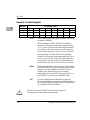
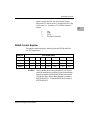
MVME172 Version Register............................................................................3-35
SCSI Interrupt Control Register.......................................................................3-36
Tick Timer 3 and 4 Compare and Counter Registers.......................................3-37
Bus Clock Register...........................................................................................3-38
PROM Access Time Control Register .............................................................3-39
Flash Access Time Control Register................................................................3-40
ABORT Switch Interrupt Control Register......................................................3-41
RESET Switch Control Register......................................................................3-42
Watchdog Timer Control Register....................................................................3-43
Access and Watchdog Time Base Select Register............................................3-44
DRAM Control Register ..................................................................................3-45
MPU Status Register........................................................................................3-46
32-bit Prescaler Count Register........................................................................3-48

xiii
CHAPTER 4 IP2 Chip
Introduction................................................................................................................4-1
Summary of Major Features...............................................................................4-1
Functional Description...............................................................................................4-2
General Description............................................................................................4-2
Cache Coherency................................................................................................4-2
Local Bus to IndustryPack DMA Controllers.....................................................4-3
Clocking Environments and Performance..........................................................4-5
Programmable Clock ..........................................................................................4-7
Error Reporting...................................................................................................4-7
Error Reporting as a Local Bus Slave .........................................................4-7
Error Reporting as a Local Bus Master .......................................................4-7
IndustryPack Error Reporting......................................................................4-8
Interrupts.............................................................................................................4-8
Overall Memory Map ................................................................................................4-9
Programming Model................................................................................................4-10
Chip ID Register...............................................................................................4-17
Chip Revision Register.....................................................................................4-17
Vector Base Register.........................................................................................4-18
IP_a, IP_b, IP_c, IP_d Memory Base Address Registers.................................4-19
IP_a or Double Size IP_ab Memory Base Address Registers ..................4-20
IP_b Memory Base Address Registers......................................................4-20
IP_c or Double Size IP_cd Memory Base Address Registers...................4-21
IP_d Memory Base Address Registers......................................................4-21
IP_a, IP_b, IP_c, IP_d Memory Size Registers................................................4-21
IP_a, IP_b, IP_c, and IP_d; IRQ0 and IRQ1 Interrupt Control Registers........4-23
IP_a, IP_b, IP_c, and IP_d; General Control Registers....................................4-24
IP Clock Register..............................................................................................4-28
DMA Arbitration Control Register...................................................................4-29
IP RESET Register ..........................................................................................4-30
Programming the DMA Controllers.................................................................4-31
DMA Enable Function...............................................................................4-33
DMA Control and Status Register Set Definition.....................................4-33
Programming the Programmable Clock....................................................4-43
Local Bus to IndustryPack Addressing....................................................................4-46
8-Bit Memory Space.........................................................................................4-46
16-Bit Memory Space.......................................................................................4-47
32-Bit Memory Space.......................................................................................4-48
IP_a I/O Space..................................................................................................4-49
IP_ab I/O Space................................................................................................4-50
IP_a ID Space ...................................................................................................4-51

xiv
IP to Local Bus Data Routing..................................................................................4-52
Memory Space Accesses..................................................................................4-52
I/O and ID Space Accesses ..............................................................................4-54
CHAPTER 5 MCECC
Introduction ...............................................................................................................5-1
Features......................................................................................................................5-1
Functional Description ..............................................................................................5-2
General Description............................................................................................5-2
Performance........................................................................................................5-2
Cache Coherency................................................................................................5-3
ECC....................................................................................................................5-4
Cycle Types.................................................................................................5-4
Error Reporting ...........................................................................................5-5
Single Bit Error (Cycle Type = Burst Read or Non-Burst Read) ...............5-5
Double Bit Error (Cycle Type = Burst Read or Non-Burst Read)..............5-5
Triple (or Greater) Bit Error
(Cycle Type = Burst Read or Non-Burst Read)..................................5-6
Cycle Type = Burst Write...........................................................................5-6
Single Bit Error (Cycle Type = Non-Burst Write)......................................5-6
Double Bit Error (Cycle Type = Non-Burst Write)....................................5-6
Triple (or Greater) Bit Error (Cycle Type = Non-Burst Write) ..................5-6
Single Bit Error (Cycle Type = Scrub) .......................................................5-6
Double Bit Error (Cycle Type = Scrub)......................................................5-7
Triple (or Greater) Bit Error (Cycle Type = Scrub)....................................5-7
Error Logging.....................................................................................................5-7
Scrub...................................................................................................................5-7
Refresh................................................................................................................5-8
Arbitration..........................................................................................................5-8
Chip Defaults......................................................................................................5-8
Programming Model..................................................................................................5-9
Chip ID Register...............................................................................................5-14
Chip Revision Register.....................................................................................5-14
Memory Configuration Register ......................................................................5-15
Dummy Register 0............................................................................................5-16
Dummy Register 1............................................................................................5-17
Base Address Register......................................................................................5-17
DRAM Control Register ..................................................................................5-18
BCLK Frequency Register...............................................................................5-20
Data Control Register.......................................................................................5-21

xv
Scrub Control Register......................................................................................5-23
Scrub Period Register Bits 15-8........................................................................5-24
Scrub Period Register Bits 7-0..........................................................................5-24
Chip Prescaler Counter.....................................................................................5-25
Scrub Time On/Time Off Register....................................................................5-25
Scrub Prescaler Counter (Bits 21-16)...............................................................5-27
Scrub Prescaler Counter (Bits 15-8).................................................................5-28
Scrub Prescaler Counter (Bits 7-0)...................................................................5-28
Scrub Timer Counter (Bits 15-8)......................................................................5-28
Scrub Timer Counter (Bits 7-0)........................................................................5-29
Scrub Address Counter (Bits 26-24).................................................................5-29
Scrub Address Counter (Bits 23-16).................................................................5-30
Scrub Address Counter (Bits 15-8)...................................................................5-30
Scrub Address Counter (Bits 7-4).....................................................................5-31
Error Logger Register.......................................................................................5-31
Error Address (Bits 31-24) ...............................................................................5-32
Error Address (Bits 23-16) ...............................................................................5-33
Error Address Bits (15-8) .................................................................................5-33
Error Address Bits (7-4) ...................................................................................5-33
Error Syndrome Register..................................................................................5-34
Defaults Register 1............................................................................................5-34
Defaults Register 2............................................................................................5-36
Initialization......................................................................................................5-37
Syndrome Decode....................................................................................................5-39
APPENDIX A Related Documentation
Motorola Computer Group Documents ....................................................................A-1
Literature Updates..............................................................................................A-2
Manufacturers’ Documents.......................................................................................A-2
APPENDIX B Using Interrupts on the MVME172
Introduction...............................................................................................................B-1
VMEchip2 Tick Timer 1 Periodic Interrupt Example ..............................................B-1
INDEX

xvi
FIGURES
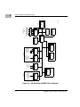
Figure 1-1. 200/300-Series MVME172 Block Diagram ...........................................1-6
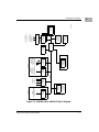
Figure 1-2. 400/500-Series MVME172 Block Diagram...........................................1-7
Figure 2-1. VMEchip2 Block Diagram.....................................................................2-5
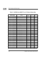
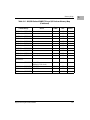
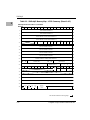
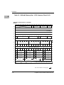
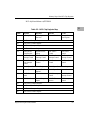
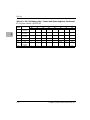
TABLES
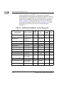
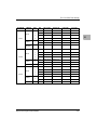
Table 1-1. MVME172 Features Summary.................................................................1-3
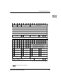
Table 1-2. Redundant Functions in the VMEchip2 and MC2 Chip .........................1-8
Table 1-3. 200/300-Series MVME172 Local Bus Memory Map............................1-10
Table 1-4. 400/500-Series MVME172 Local Bus Memory Map............................1-12
Table 1-5. 200/300-Series MVME172 Local I/O Devices Memory Map...............1-14
Table 1-6. 400/500-Series MVME172 Local I/O Devices Memory Map...............1-18
Table 1-7. VMEchip2 Memory Map (Sheet 1 of 3) ................................................1-22
Table 1-8. MC2 Chip Register Map ........................................................................1-27
Table 1-9. IP2 Chip Overall Memory Map..............................................................1-28
Table 1-10. IP2 Chip Memory Map - Control and Status Registers .......................1-29
Table 1-11. MCECC Internal Register Memory Map ............................................1-35
Table 1-12. Z85230 SCC Register Addresses .........................................................1-37
Table 1-13. 82596CA Ethernet LAN Memory Map................................................1-38
Table 1-14. 53C710 SCSI Memory Map ...............................................................1-39
Table 1-15. MK48T58 BBRAM/TOD Clock Memory Map...................................1-40
Table 1-16. BBRAM Configuration Area Memory Map .......................................1-41
Table 1-17. TOD Clock Memory Map ....................................................................1-42
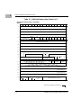
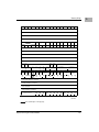
Table 2-1. VMEchip2 Memory Map - LCSR Summary (Sheet 1 of 2) ..................2-22
Table 2-2. DMAC Command Table Format............................................................2-53
Table 2-3. Local Bus Interrupter Summary ............................................................2-76
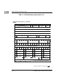
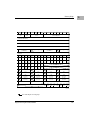
Table 2-4. VMEchip2 Memory Map (GCSR Summary) ......................................2-104
Table 3-1. DRAM Performance.................................................................................3-6
Table 3-2. MC2 Chip Register Map .........................................................................3-9
Table 3-3. Interrupt Vector Base Register Encoding and Priority...........................3-14
Table 3-4. DRAM Size Control Bit Encoding.........................................................3-27
Table 3-5. DRAM Size Control Bit Encoding.........................................................3-28
Table 3-6. SRAM Size Control Bit Encoding .........................................................3-28
Table 3-7. SRAM Size Control Bit Encoding .........................................................3-29
Table 4-1. IP2 Chip Clock Cycles.............................................................................4-6
Table 4-2. IP2 Chip Overall Memory Map ...............................................................4-9
Table 4-3. IP2 Chip Memory Map - Control and Status Registers .........................4-11

xvii
Table 5-1. MCECC Specifications.............................................................................5-3
Table 5-2. MCECC Internal Register Memory Map, Part 1....................................5-10
Table 5-3. MCECC Internal Register Memory Map, Part 2 ...................................5-12
Table A-1. Motorola Computer Group Documents..................................................A-1
Table A-2. Manufacturers’ Documents ....................................................................A-2

xviii

1-1
1
1Board Description
and Memory Maps
Introduction
This manual provides programming information for the MVME172
Embedded Controller. Extensive programming information is provided for
the Application-Specific Integrated Circuit (ASIC) devices used on the
board. Reference information is included for the Large Scale Integration
(LSI) devices used on the board and sources for additional information are
provided.
This chapter briefly describes the board level hardware features of the
MVME172 Embedded Controller. The chapter begins with a board level
overview and features list. Memory maps are next, and the chapter closes
with some general software considerations such as cache coherency,
interrupts, and bus errors.
All programmable registers in the MVME172 that reside in ASICs are
covered in the chapters on those ASICs. Chapter 2 covers the VMEchip2,
Chapter 3 covers the MC2 chip, and Chapter 4 covers the IP2 chip. Chapter
5 covers the MCECC chip, used only on 200/300-Series MVME172.
Appendix A describes using interrupts. For those interested in
programmable register bit definitions and less interested in hardware
functionality, focus on Chapters 2, 3, 4, and 5. In some cases, however,
Chapter 1 gives related background information.
Overview
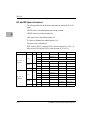
The MVME172 is based on the MC68060 or MC68LC060
microprocessor. The MVME172 is available in various versions with the
features listed in Table 1-1 on page 1-3. A “No VMEbus” option is also
available.
The I/O connection for the 200/300-Series MVME172 is provided through
four RJ-45 front panel connectors.

1-2 Computer Group Literature Center Web Site
Board Description and Memory Maps
1
The I/O connection for the 400/500-Series serial ports is provided by two
DB-25 front panel I/O connectors. The I/O is connected to the VMEbus P2
connector. The main board is connected through a P2 transition board and
cables to transition boards. The Series 400/500 MVME172 supports the
transition boards MVME712-12, MVME712-13, MVME712M,
MVME712A, MVME712AM, and MVME712B (referred to in this
manual as MVME712x, unless separately specified). These transition
boards provide configuration headers, serial port drivers and industry
standard connectors for the I/O devices. The MVME712 series transition
boards were designed to support the MVME167 boards, but can be used
on the MVME172 by following some special precautions. (Refer to the
section on the Serial Communications Interface in the MVME172
installation and use manual furnished with your 400/500-Series
MVME172, for more information.)
The VMEbus interface is provided by an ASIC called the VMEchip2. The
VMEchip2 includes two tick timers, a watchdog timer, programmable map
decoders for the master and slave interfaces, and a VMEbus to/from local
bus DMA controller, a VMEbus to/from local bus non-DMA programmed
access interface, a VMEbus interrupter, a VMEbus system controller, a
VMEbus interrupt handler, and a VMEbus requester.
Processor-to-VMEbus transfers can be D8, D16, or D32. VMEchip2 DMA
transfers to the VMEbus, however, can be D16, D32, D16/BLT, D32/BLT,
or D64/MBLT.
The MC2 chip ASIC provides four tick timers, the interface to the LAN
chip, SCSI chip, serial port chip, BBRAM, the programmable interface for
the DRAM and/or SRAM mezzanine board, and Flash write enable.
The IndustryPack Interface Controller (IP2 chip) ASIC provides control
and status information, including DMA control, for up to four single size
IndustryPacks (IPs) or up to two double size IPs that can be plugged into
the MVME172 main module.
Page is loading ...
Page is loading ...
Page is loading ...
Page is loading ...
Page is loading ...
Page is loading ...
Page is loading ...
Page is loading ...
Page is loading ...
Page is loading ...
Page is loading ...
Page is loading ...
Page is loading ...
Page is loading ...
Page is loading ...
Page is loading ...
Page is loading ...
Page is loading ...
Page is loading ...
Page is loading ...
Page is loading ...
Page is loading ...
Page is loading ...
Page is loading ...
Page is loading ...
Page is loading ...
Page is loading ...
Page is loading ...
Page is loading ...
Page is loading ...
Page is loading ...
Page is loading ...
Page is loading ...
Page is loading ...
Page is loading ...
Page is loading ...
Page is loading ...
Page is loading ...
Page is loading ...
Page is loading ...
Page is loading ...
Page is loading ...
Page is loading ...
Page is loading ...
Page is loading ...
Page is loading ...
Page is loading ...
Page is loading ...
Page is loading ...
Page is loading ...
Page is loading ...
Page is loading ...
Page is loading ...
Page is loading ...
Page is loading ...
Page is loading ...
Page is loading ...
Page is loading ...
Page is loading ...
Page is loading ...
Page is loading ...
Page is loading ...
Page is loading ...
Page is loading ...
Page is loading ...
Page is loading ...
Page is loading ...
Page is loading ...
Page is loading ...
Page is loading ...
Page is loading ...
Page is loading ...
Page is loading ...
Page is loading ...
Page is loading ...
Page is loading ...
Page is loading ...
Page is loading ...
Page is loading ...
Page is loading ...
Page is loading ...
Page is loading ...
Page is loading ...
Page is loading ...
Page is loading ...
Page is loading ...
Page is loading ...
Page is loading ...
Page is loading ...
Page is loading ...
Page is loading ...
Page is loading ...
Page is loading ...
Page is loading ...
Page is loading ...
Page is loading ...
Page is loading ...
Page is loading ...
Page is loading ...
Page is loading ...
Page is loading ...
Page is loading ...
Page is loading ...
Page is loading ...
Page is loading ...
Page is loading ...
Page is loading ...
Page is loading ...
Page is loading ...
Page is loading ...
Page is loading ...
Page is loading ...
Page is loading ...
Page is loading ...
Page is loading ...
Page is loading ...
Page is loading ...
Page is loading ...
Page is loading ...
Page is loading ...
Page is loading ...
Page is loading ...
Page is loading ...
Page is loading ...
Page is loading ...
Page is loading ...
Page is loading ...
Page is loading ...
Page is loading ...
Page is loading ...
Page is loading ...
Page is loading ...
Page is loading ...
Page is loading ...
Page is loading ...
Page is loading ...
Page is loading ...
Page is loading ...
Page is loading ...
Page is loading ...
Page is loading ...
Page is loading ...
Page is loading ...
Page is loading ...
Page is loading ...
Page is loading ...
Page is loading ...
Page is loading ...
Page is loading ...
Page is loading ...
Page is loading ...
Page is loading ...
Page is loading ...
Page is loading ...
Page is loading ...
Page is loading ...
Page is loading ...
Page is loading ...
Page is loading ...
Page is loading ...
Page is loading ...
Page is loading ...
Page is loading ...
Page is loading ...
Page is loading ...
Page is loading ...
Page is loading ...
Page is loading ...
Page is loading ...
Page is loading ...
Page is loading ...
Page is loading ...
Page is loading ...
Page is loading ...
Page is loading ...
Page is loading ...
Page is loading ...
Page is loading ...
Page is loading ...
Page is loading ...
Page is loading ...
Page is loading ...
Page is loading ...
Page is loading ...
Page is loading ...
Page is loading ...
Page is loading ...
Page is loading ...
Page is loading ...
Page is loading ...
Page is loading ...
Page is loading ...
Page is loading ...
Page is loading ...
Page is loading ...
Page is loading ...
Page is loading ...
Page is loading ...
Page is loading ...
Page is loading ...
Page is loading ...
Page is loading ...
Page is loading ...
Page is loading ...
Page is loading ...
Page is loading ...
Page is loading ...
Page is loading ...
Page is loading ...
Page is loading ...
Page is loading ...
Page is loading ...
Page is loading ...
Page is loading ...
Page is loading ...
Page is loading ...
Page is loading ...
Page is loading ...
Page is loading ...
Page is loading ...
Page is loading ...
Page is loading ...
Page is loading ...
Page is loading ...
Page is loading ...
Page is loading ...
Page is loading ...
Page is loading ...
Page is loading ...
Page is loading ...
Page is loading ...
Page is loading ...
Page is loading ...
Page is loading ...
Page is loading ...
Page is loading ...
Page is loading ...
Page is loading ...
Page is loading ...
Page is loading ...
Page is loading ...
Page is loading ...
Page is loading ...
Page is loading ...
Page is loading ...
Page is loading ...
Page is loading ...
Page is loading ...
Page is loading ...
Page is loading ...
Page is loading ...
Page is loading ...
Page is loading ...
Page is loading ...
Page is loading ...
Page is loading ...
Page is loading ...
Page is loading ...
Page is loading ...
Page is loading ...
Page is loading ...
Page is loading ...
Page is loading ...
Page is loading ...
Page is loading ...
Page is loading ...
Page is loading ...
Page is loading ...
Page is loading ...
Page is loading ...
Page is loading ...
Page is loading ...
Page is loading ...
Page is loading ...
Page is loading ...
Page is loading ...
Page is loading ...
Page is loading ...
Page is loading ...
Page is loading ...
Page is loading ...
Page is loading ...
Page is loading ...
Page is loading ...
Page is loading ...
Page is loading ...
Page is loading ...
Page is loading ...
Page is loading ...
Page is loading ...
Page is loading ...
Page is loading ...
Page is loading ...
Page is loading ...
Page is loading ...
Page is loading ...
Page is loading ...
Page is loading ...
Page is loading ...
Page is loading ...
Page is loading ...
Page is loading ...
Page is loading ...
Page is loading ...
Page is loading ...
Page is loading ...
Page is loading ...
Page is loading ...
Page is loading ...
Page is loading ...
Page is loading ...
Page is loading ...
Page is loading ...
Page is loading ...
Page is loading ...
Page is loading ...
Page is loading ...
Page is loading ...
Page is loading ...
Page is loading ...
Page is loading ...
Page is loading ...
Page is loading ...
Page is loading ...
Page is loading ...
Page is loading ...
Page is loading ...
Page is loading ...
Page is loading ...
Page is loading ...
Page is loading ...
Page is loading ...
Page is loading ...
Page is loading ...
-
 1
1
-
 2
2
-
 3
3
-
 4
4
-
 5
5
-
 6
6
-
 7
7
-
 8
8
-
 9
9
-
 10
10
-
 11
11
-
 12
12
-
 13
13
-
 14
14
-
 15
15
-
 16
16
-
 17
17
-
 18
18
-
 19
19
-
 20
20
-
 21
21
-
 22
22
-
 23
23
-
 24
24
-
 25
25
-
 26
26
-
 27
27
-
 28
28
-
 29
29
-
 30
30
-
 31
31
-
 32
32
-
 33
33
-
 34
34
-
 35
35
-
 36
36
-
 37
37
-
 38
38
-
 39
39
-
 40
40
-
 41
41
-
 42
42
-
 43
43
-
 44
44
-
 45
45
-
 46
46
-
 47
47
-
 48
48
-
 49
49
-
 50
50
-
 51
51
-
 52
52
-
 53
53
-
 54
54
-
 55
55
-
 56
56
-
 57
57
-
 58
58
-
 59
59
-
 60
60
-
 61
61
-
 62
62
-
 63
63
-
 64
64
-
 65
65
-
 66
66
-
 67
67
-
 68
68
-
 69
69
-
 70
70
-
 71
71
-
 72
72
-
 73
73
-
 74
74
-
 75
75
-
 76
76
-
 77
77
-
 78
78
-
 79
79
-
 80
80
-
 81
81
-
 82
82
-
 83
83
-
 84
84
-
 85
85
-
 86
86
-
 87
87
-
 88
88
-
 89
89
-
 90
90
-
 91
91
-
 92
92
-
 93
93
-
 94
94
-
 95
95
-
 96
96
-
 97
97
-
 98
98
-
 99
99
-
 100
100
-
 101
101
-
 102
102
-
 103
103
-
 104
104
-
 105
105
-
 106
106
-
 107
107
-
 108
108
-
 109
109
-
 110
110
-
 111
111
-
 112
112
-
 113
113
-
 114
114
-
 115
115
-
 116
116
-
 117
117
-
 118
118
-
 119
119
-
 120
120
-
 121
121
-
 122
122
-
 123
123
-
 124
124
-
 125
125
-
 126
126
-
 127
127
-
 128
128
-
 129
129
-
 130
130
-
 131
131
-
 132
132
-
 133
133
-
 134
134
-
 135
135
-
 136
136
-
 137
137
-
 138
138
-
 139
139
-
 140
140
-
 141
141
-
 142
142
-
 143
143
-
 144
144
-
 145
145
-
 146
146
-
 147
147
-
 148
148
-
 149
149
-
 150
150
-
 151
151
-
 152
152
-
 153
153
-
 154
154
-
 155
155
-
 156
156
-
 157
157
-
 158
158
-
 159
159
-
 160
160
-
 161
161
-
 162
162
-
 163
163
-
 164
164
-
 165
165
-
 166
166
-
 167
167
-
 168
168
-
 169
169
-
 170
170
-
 171
171
-
 172
172
-
 173
173
-
 174
174
-
 175
175
-
 176
176
-
 177
177
-
 178
178
-
 179
179
-
 180
180
-
 181
181
-
 182
182
-
 183
183
-
 184
184
-
 185
185
-
 186
186
-
 187
187
-
 188
188
-
 189
189
-
 190
190
-
 191
191
-
 192
192
-
 193
193
-
 194
194
-
 195
195
-
 196
196
-
 197
197
-
 198
198
-
 199
199
-
 200
200
-
 201
201
-
 202
202
-
 203
203
-
 204
204
-
 205
205
-
 206
206
-
 207
207
-
 208
208
-
 209
209
-
 210
210
-
 211
211
-
 212
212
-
 213
213
-
 214
214
-
 215
215
-
 216
216
-
 217
217
-
 218
218
-
 219
219
-
 220
220
-
 221
221
-
 222
222
-
 223
223
-
 224
224
-
 225
225
-
 226
226
-
 227
227
-
 228
228
-
 229
229
-
 230
230
-
 231
231
-
 232
232
-
 233
233
-
 234
234
-
 235
235
-
 236
236
-
 237
237
-
 238
238
-
 239
239
-
 240
240
-
 241
241
-
 242
242
-
 243
243
-
 244
244
-
 245
245
-
 246
246
-
 247
247
-
 248
248
-
 249
249
-
 250
250
-
 251
251
-
 252
252
-
 253
253
-
 254
254
-
 255
255
-
 256
256
-
 257
257
-
 258
258
-
 259
259
-
 260
260
-
 261
261
-
 262
262
-
 263
263
-
 264
264
-
 265
265
-
 266
266
-
 267
267
-
 268
268
-
 269
269
-
 270
270
-
 271
271
-
 272
272
-
 273
273
-
 274
274
-
 275
275
-
 276
276
-
 277
277
-
 278
278
-
 279
279
-
 280
280
-
 281
281
-
 282
282
-
 283
283
-
 284
284
-
 285
285
-
 286
286
-
 287
287
-
 288
288
-
 289
289
-
 290
290
-
 291
291
-
 292
292
-
 293
293
-
 294
294
-
 295
295
-
 296
296
-
 297
297
-
 298
298
-
 299
299
-
 300
300
-
 301
301
-
 302
302
-
 303
303
-
 304
304
-
 305
305
-
 306
306
-
 307
307
-
 308
308
-
 309
309
-
 310
310
-
 311
311
-
 312
312
-
 313
313
-
 314
314
-
 315
315
-
 316
316
-
 317
317
-
 318
318
-
 319
319
-
 320
320
-
 321
321
-
 322
322
-
 323
323
-
 324
324
-
 325
325
-
 326
326
-
 327
327
-
 328
328
-
 329
329
-
 330
330
-
 331
331
-
 332
332
-
 333
333
-
 334
334
-
 335
335
-
 336
336
-
 337
337
-
 338
338
-
 339
339
-
 340
340
-
 341
341
-
 342
342
-
 343
343
-
 344
344
-
 345
345
-
 346
346
-
 347
347
-
 348
348
-
 349
349
-
 350
350
-
 351
351
-
 352
352
-
 353
353
-
 354
354


Ask a question and I''ll find the answer in the document
Finding information in a document is now easier with AI
Related papers
-
Motorola MVME1X7P Datasheet
-
-
-
-
-
-
-
-
Motorola MVME2400-0331 Installation and Use Manual
-
Other documents
-
CH Tech AMi4000 User manual
-
TEWS TVME200 User manual
-
-
Hitachi SH7095 Hardware User Manual
-
 ARMTEL TOP-EC-IP2 User manual
-
-
National Instruments Printer Accessories 320030-01 User manual
-
ESD VME-ISER8 Owner's manual
-
Emerson MVME3100 User manual
-
