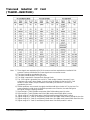
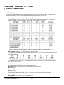
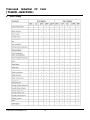
Transcend Industrial Ultra Speed CF Card User manual
- Category
- Memory cards
- Type
- User manual
This manual is also suitable for

T
T
T
r
r
r
a
a
a
n
n
n
s
s
s
c
c
c
e
e
e
n
n
n
d
d
d
I
I
I
n
n
n
d
d
d
u
u
u
s
s
s
t
t
t
r
r
r
i
i
i
a
a
a
l
l
l
C
C
C
F
F
F
C
C
C
a
a
a
r
r
r
d
d
d
(
(
(
T
T
T
S
S
S
1
1
1
2
2
2
8
8
8
M
M
M
~
~
~
8
8
8
G
G
G
B
B
B
C
C
C
F
F
F
1
1
1
0
0
0
0
0
0
I
I
I
)
)
)
Transcend Information Inc.
1
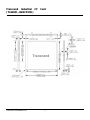
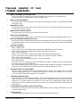
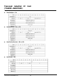
Description
The Transcend CF100I is a High Speed industrial
Compact Flash Card with high quality Flash Memory
assembled on a printed circuit board.
Placement
Features
• CompactFlash Specification Version 4.1 Complaint
• RoHS compliant products
• Single Power Supply: 3.3V±5% or 5V±10%
• Operating Temperature: -40
o
C to 85
o
C
• Storage Temperature: -55
o
C to 100
o
C
• Operation Modes:
PC Card Memory Mode
PC Card IO Mode
True IDE Mode
• True IDE Mode supports up to Ultra DMA Mode 4
• Support PIO mode 0 to PIO mode 6
• True IDE Mode: Fixed Disk (Standard)
• PC Card Mode: Fixed Disk (Standard)
• Durability of Connector: 10,000 times
• Endurance: 2,000,000 Program/Erase cycles
• MTBF: 1,000,000 hours
• Support Wear-Leveling to extend product life
• Compliant to CompactFlash, PCMCIA, and ATA
standards
Dimensions

T
T
T
r
r
r
a
a
a
n
n
n
s
s
s
c
c
c
e
e
e
n
n
n
d
d
d
I
I
I
n
n
n
d
d
d
u
u
u
s
s
s
t
t
t
r
r
r
i
i
i
a
a
a
l
l
l
C
C
C
F
F
F
C
C
C
a
a
a
r
r
r
d
d
d
(
(
(
T
T
T
S
S
S
1
1
1
2
2
2
8
8
8
M
M
M
~
~
~
8
8
8
G
G
G
B
B
B
C
C
C
F
F
F
1
1
1
0
0
0
0
0
0
I
I
I
)
)
)
Transcend Information Inc.
2
Transcend

T
T
T
r
r
r
a
a
a
n
n
n
s
s
s
c
c
c
e
e
e
n
n
n
d
d
d
I
I
I
n
n
n
d
d
d
u
u
u
s
s
s
t
t
t
r
r
r
i
i
i
a
a
a
l
l
l
C
C
C
F
F
F
C
C
C
a
a
a
r
r
r
d
d
d
(
(
(
T
T
T
S
S
S
1
1
1
2
2
2
8
8
8
M
M
M
~
~
~
8
8
8
G
G
G
B
B
B
C
C
C
F
F
F
1
1
1
0
0
0
0
0
0
I
I
I
)
)
)
Transcend Information Inc.
3
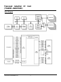
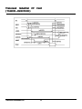
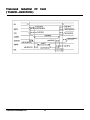
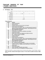
Block Diagram

T
T
T
r
r
r
a
a
a
n
n
n
s
s
s
c
c
c
e
e
e
n
n
n
d
d
d
I
I
I
n
n
n
d
d
d
u
u
u
s
s
s
t
t
t
r
r
r
i
i
i
a
a
a
l
l
l
C
C
C
F
F
F
C
C
C
a
a
a
r
r
r
d
d
d
(
(
(
T
T
T
S
S
S
1
1
1
2
2
2
8
8
8
M
M
M
~
~
~
8
8
8
G
G
G
B
B
B
C
C
C
F
F
F
1
1
1
0
0
0
0
0
0
I
I
I
)
)
)
Transcend Information Inc.
4
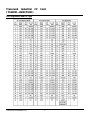
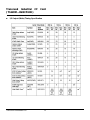
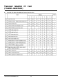
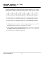
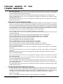
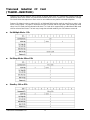
Pin Assignments and Pin Type

T
T
T
r
r
r
a
a
a
n
n
n
s
s
s
c
c
c
e
e
e
n
n
n
d
d
d
I
I
I
n
n
n
d
d
d
u
u
u
s
s
s
t
t
t
r
r
r
i
i
i
a
a
a
l
l
l
C
C
C
F
F
F
C
C
C
a
a
a
r
r
r
d
d
d
(
(
(
T
T
T
S
S
S
1
1
1
2
2
2
8
8
8
M
M
M
~
~
~
8
8
8
G
G
G
B
B
B
C
C
C
F
F
F
1
1
1
0
0
0
0
0
0
I
I
I
)
)
)
Transcend Information Inc.
5
Note: 1) These signals are required only for 16 bit accesses and not required when installed in 8 bit
systems. Devices should allow for 3-state signals not to consume current.
2) The signal should be grounded by the host.
3) The signal should be tied to VCC by the host.
4) The mode is required for CompactFlash Storage Cards.
5) The -CSEL signal is ignored by the card in PC Card modes. However, because it is not
pulled upon the card in these modes, it should not be left floating by the host in PC Card
modes. In these modes, the pin should be connected by the host to PC Card A25 or
grounded by the host.
6) If DMA operations are not used, the signal should be held high or tied to VCC by the host. For
proper operation in older hosts: while DMA operations are not active, the card shall ignore
this signal,including a floating condition
7) Signal usage in True IDE Mode except when Ultra DMA mode protocol is active.
8) Signal usage in True IDE Mode when Ultra DMA mode protocol DMA Write is active.
9) Signal usage in True IDE Mode when Ultra DMA mode protocol DMA Read is active.
10) Signal usage in PC Card I/O and Memory Mode when Ultra DMA mode protocol DMA Write is active.
11) Signal usage in PC Card I/O and Memory Mode when Ultra DMA mode protocol DMA Read is active.
12) Signal usage in PC Card I/O and Memory Mode when Ultra DMA protocol is active.

T
T
T
r
r
r
a
a
a
n
n
n
s
s
s
c
c
c
e
e
e
n
n
n
d
d
d
I
I
I
n
n
n
d
d
d
u
u
u
s
s
s
t
t
t
r
r
r
i
i
i
a
a
a
l
l
l
C
C
C
F
F
F
C
C
C
a
a
a
r
r
r
d
d
d
(
(
(
T
T
T
S
S
S
1
1
1
2
2
2
8
8
8
M
M
M
~
~
~
8
8
8
G
G
G
B
B
B
C
C
C
F
F
F
1
1
1
0
0
0
0
0
0
I
I
I
)
)
)
Transcend Information Inc.
6
Signal Description
Signal Name Dir. Pin Description
A10 – A00
(PC Card Memory Mode)
A10 – A00
(PC Card I/O Mode)
A02 - A00
(True IDE Mode)
I
I
8,10,11,12,
14,15,16,17,
18,19,20
18,19,20
These address lines along with the -REG signal are used to select the following:
The I/O port address registers within the CompactFlash Storage Card , the
memory mapped port address registers within the CompactFlash Storage Card,
a byte in the card's information structure and its configuration control and status
registers.
This signal is the same as the PC Card Memory Mode signal.
In True IDE Mode, only A[02:00] are used to select the one of eight registers
in the Task File, the remaining address lines should be grounded by the host.
BVD1
(PC Card Memory Mode)
-STSCHG
(PC Card I/O Mode)
Status Changed
-PDIAG
(True IDE Mode)
I/O 46 This signal is asserted high, as BVD1 is not supported.
This signal is asserted low to alert the host to changes in the READY and Write
Protect states, while the I/O interface is configured. Its use is controlled by the
Card Config and Status Register.
In the True IDE Mode, this input / output is the Pass Diagnostic signal in the
Master / Slave handshake protocol.
BVD2
(PC Card Memory Mode)
-SPKR
(PC Card I/O Mode)
-DASP
(True IDE Mode)
I/O 45 This signal is asserted high, as BVD2 is not supported.
This line is the Binary Audio output from the card. If the Card does not support
the Binary Audio function, this line should be held negated.
In the True IDE Mode, this input/output is the Disk Active/Slave Present signal in
the Master/Slave handshake protocol.
-CD1, -CD2
(PC Card Memory Mode)
-CD1, -CD2
(PC Card I/O Mode)
-CD1, -CD2
(True IDE Mode)
O 26,25 These Card Detect pins are connected to ground on the CompactFlash Storage
Card. They are used by the host to determine that the CompactFlash Storage
Card is fully inserted into its socket.
This signal is the same for all modes.
This signal is the same for all modes.

T
T
T
r
r
r
a
a
a
n
n
n
s
s
s
c
c
c
e
e
e
n
n
n
d
d
d
I
I
I
n
n
n
d
d
d
u
u
u
s
s
s
t
t
t
r
r
r
i
i
i
a
a
a
l
l
l
C
C
C
F
F
F
C
C
C
a
a
a
r
r
r
d
d
d
(
(
(
T
T
T
S
S
S
1
1
1
2
2
2
8
8
8
M
M
M
~
~
~
8
8
8
G
G
G
B
B
B
C
C
C
F
F
F
1
1
1
0
0
0
0
0
0
I
I
I
)
)
)
Transcend Information Inc.
7
Signal Name Dir. Pin Description
-CE1, -CE2
(PC Card Memory Mode)
Card Enable
-CE1, -CE2
(PC Card I/O Mode)
Card Enable
-CS0, -CS1
(True IDE Mode)
I 7,32
These input signals are used both to select the card and to indicate to the card
whether a byte or a word operation is being performed. -CE2 always accesses
the odd byte of the word.-CE1 accesses the even byte or the Odd byte of the
word depending on A0 and -CE2. A multiplexing scheme based on A0,-CE1,
-CE2 allows 8 bit hosts to access all data on D0-D7. See Table 27, Table 29,
Table 31, Table 35, Table 36 and Table 37.
This signal is the same as the PC Card Memory Mode signal.
In the True IDE Mode, -CS0 is the address range select for the task file
registers while -CS1 is used to select the Alternate Status Register and the
Device Control Register.
While –DMACK is asserted, -CS0 and –CS1 shall be held negated and the
width of the transfers shall be 16 bits.
-CSEL
(PC Card Memory Mode)
-CSEL
(PC Card I/O Mode)
-CSEL
(True IDE Mode)
I 39 This signal is not used for this mode, but should be connected by the host to PC
Card A25 or grounded by the host.
This signal is not used for this mode, but should be connected by the host to PC
Card A25 or grounded by the host.
This internally pulled up signal is used to configure this device as a Master or a
Slave when configured in the True IDE Mode.
When this pin is grounded, this device is configured as a Master.
When the pin is open, this device is configured as a Slave.
D15 - D00
(PC Card Memory Mode)
D15 - D00
(PC Card I/O Mode)
D15 - D00
(True IDE Mode)
I/O
31,30,29,28,
27,49,48,47,
6,5,4,3,2,
23, 22, 21
These lines carry the Data, Commands and Status information between the host
and the controller. D00 is the LSB of the Even Byte of the Word. D08 is the LSB
of the Odd Byte of the Word.
This signal is the same as the PC Card Memory Mode signal.
In True IDE Mode, all Task File operations occur in byte mode on the low order
bus D[7:0] while all data transfers are 16 bit using D[15:0].
GND
(PC Card Memory Mode)
GND
(PC Card I/O Mode)
GND
(True IDE Mode)
-- 1,50 Ground.
This signal is the same for all modes.
This signal is the same for all modes.

T
T
T
r
r
r
a
a
a
n
n
n
s
s
s
c
c
c
e
e
e
n
n
n
d
d
d
I
I
I
n
n
n
d
d
d
u
u
u
s
s
s
t
t
t
r
r
r
i
i
i
a
a
a
l
l
l
C
C
C
F
F
F
C
C
C
a
a
a
r
r
r
d
d
d
(
(
(
T
T
T
S
S
S
1
1
1
2
2
2
8
8
8
M
M
M
~
~
~
8
8
8
G
G
G
B
B
B
C
C
C
F
F
F
1
1
1
0
0
0
0
0
0
I
I
I
)
)
)
Transcend Information Inc.
8
Signal Name Dir. Pin Description
-INPACK
(PC Card Memory Mode)
-INPACK
(PC Card I/O Mode)
Input Acknowledge
DMARQ
(True IDE Mode)
O 43 This signal is not used in this mode.
The Input Acknowledge signal is asserted by the CompactFlash Storage Card
when the card is selected and responding to an I/O read cycle at the address that
is on the address bus. This signal is used by the host to control the enable of any
input data buffers between the CompactFlash Storage Card and the CPU.
This signal is a DMA Request that is used for DMA data transfers between host
and device. It shall be asserted by the device when it is ready to transfer data to
or from the host. For Multiword DMA transfers, the direction of data transfer is
controlled by -IORD and -IOWR. This signal is used in a handshake manner with
-DMACK, i.e., the device shall wait until the host asserts -DMACK before
negating DMARQ, and reasserting DMARQ if there is more data to transfer.
DMARQ shall not be driven when the device is not selected.
While a DMA operation is in progress, -CS0 and –CS1 shall be held negated and
the width of the transfers shall be 16 bits.
If there is no hardware support for DMA mode in the host, this output signal is not
used and should not be connected at the host. In this case, the BIOS must report
that DMA mode is not supported by the host so that device drivers will not
attempt DMA mode.
A host that does not support DMA mode and implements both PCMCIA and
True-IDE modes of operation need not alter the PCMCIA mode connections
while in True-IDE mode as long as this does not prevent proper operation in any
mode.
-IORD
(PC Card Memory Mode)
-IORD
(PC Card I/O Mode)
-IORD
(True IDE Mode – Except
Ultra DMA Protocol Active)
-HDMARDY
(True IDE Mode – In Ultra
DMA Protocol DMA Read)
HSTROBE
(True IDE Mode – In Ultra
DMA Protocol DMA Write)
I 34 This signal is not used in this mode.
This is an I/O Read strobe generated by the host. This signal gates I/O data onto
the bus from the CompactFlash Storage Card when the card is configured to use
the I/O interface.
In True IDE Mode, while Ultra DMA mode is not active, this signal has the same
function as in PC Card I/O Mode.
In True IDE Mode when Ultra DMA mode DMA Read is active, this signal is
asserted by the host to indicate that the host is read to receive Ultra DMA data-in
bursts. The host may negate -HDMARDY to pause an Ultra DMA transfer.
In True IDE Mode when Ultra DMA mode DMA Write is active, this signal is the
data out strobe generated by the host. Both the rising and falling edge of
HSTROBE cause data to be latched by the device. The host may stop
generating HSTROBE edges to pause an Ultra DMA data-out burst.

T
T
T
r
r
r
a
a
a
n
n
n
s
s
s
c
c
c
e
e
e
n
n
n
d
d
d
I
I
I
n
n
n
d
d
d
u
u
u
s
s
s
t
t
t
r
r
r
i
i
i
a
a
a
l
l
l
C
C
C
F
F
F
C
C
C
a
a
a
r
r
r
d
d
d
(
(
(
T
T
T
S
S
S
1
1
1
2
2
2
8
8
8
M
M
M
~
~
~
8
8
8
G
G
G
B
B
B
C
C
C
F
F
F
1
1
1
0
0
0
0
0
0
I
I
I
)
)
)
Transcend Information Inc.
9
Signal Name Dir. Pin Description
-IOWR
(PC Card Memory Mode)
-IOWR
(PC Card I/O Mode)
-IOWR
(True IDE Mode – Except
Ultra DMA Protocol Active)
STOP
(True IDE Mode – Ultra DMA
Protocol Active)
I 35
This signal is not used in this mode.
The I/O Write strobe pulse is used to clock I/O data on the Card Data bus into the
CompactFlash Storage Card controller registers when the CompactFlash
Storage Card is configured to use the I/O interface.
The clocking shall occur on the negative to positive edge of the signal (trailing
edge).
In True IDE Mode, while Ultra DMA mode protocol is not active, this signal has
the same function as in PC Card I/O Mode. When Ultra DMA mode protocol is
supported, this signal must be negated before entering Ultra DMA mode
protocol.
In True IDE Mode, while Ultra DMA mode protocol is active, the assertion of this
signal causes the termination of the Ultra DMA burst.
-OE
(PC Card Memory Mode)
-OE
(PC Card I/O Mode)
-ATA SEL
(True IDE Mode)
I 9
This is an Output Enable strobe generated by the host interface. It is used to read
data from the CompactFlash Storage Card in Memory Mode and to read the CIS
and configuration registers.
In PC Card I/O Mode, this signal is used to read the CIS and configuration
registers.
To enable True IDE Mode this input should be grounded by the host.
READY
(PC Card Memory Mode)
-IREQ
(PC Card I/O Mode)
INTRQ
(True IDE Mode)
O 37
In Memory Mode, this signal is set high when the CompactFlash Storage Card is
ready to accept a new data transfer operation and is held low when the card is
busy.
At power up and at Reset, the READY signal is held low (busy) until the
CompactFlash Storage Card has completed its power up or reset function. No
access of any type should be made to the CompactFlash Storage Card during
this time.
Note, however, that when a card is powered up and used with RESET
continuously disconnected or asserted, the Reset function of the RESET pin is
disabled. Consequently, the continuous assertion of RESET from the application
of power shall not cause the READY signal to remain continuously in the busy
state.
I/O Operation – After the CompactFlash Storage Card Card has been configured
for I/O operation, this signal is used as -Interrupt Request. This line is strobed
low to generate a pulse mode interrupt or held low for a level mode interrupt.
In True IDE Mode signal is the active high Interrupt Request to the host.

T
T
T
r
r
r
a
a
a
n
n
n
s
s
s
c
c
c
e
e
e
n
n
n
d
d
d
I
I
I
n
n
n
d
d
d
u
u
u
s
s
s
t
t
t
r
r
r
i
i
i
a
a
a
l
l
l
C
C
C
F
F
F
C
C
C
a
a
a
r
r
r
d
d
d
(
(
(
T
T
T
S
S
S
1
1
1
2
2
2
8
8
8
M
M
M
~
~
~
8
8
8
G
G
G
B
B
B
C
C
C
F
F
F
1
1
1
0
0
0
0
0
0
I
I
I
)
)
)
Transcend Information Inc.
10
Signal Name Dir. Pin Description
-REG
(PC Card Memory Mode)
Attribute Memory Select
-REG
(PC Card I/O Mode)
I 44
This signal is used during Memory Cycles to distinguish between Common
Memory and Register (Attribute) Memory accesses. High for Common Memory,
Low for Attribute Memory.
The signal shall also be active (low) during I/O Cycles when the I/O address is on
the Bus.
-DMACK
(True IDE Mode)
This is a DMA Acknowledge signal that is asserted by the host in response to
DMARQ to initiate DMA transfers.
While DMA operations are not active, the card shall ignore the -DMACK signal,
including a floating condition.
If DMA operation is not supported by a True IDE Mode only host, this signal
should be driven high or connected to VCC by the host.
A host that does not support DMA mode and implements both PCMCIA and
True-IDE modes of operation need not alter the PCMCIA mode connections
while in True-IDE mode as long as this does not prevent proper operation all
modes.
RESET
(PC Card Memory Mode)
RESET
(PC Card I/O Mode)
-RESET
(True IDE Mode)
I 41 The CompactFlash Storage Card is Reset when the RESET pin is high with the
following important exception:
The host may leave the RESET pin open or keep it continually high from the
application of power without causing a continuous Reset of the card. Under
either of these conditions, the card shall emerge from power-up having
completed an initial Reset.
The CompactFlash Storage Card is also Reset when the Soft Reset bit in the
Card Configuration Option Register is set.
This signal is the same as the PC Card Memory Mode signal.
In the True IDE Mode, this input pin is the active low hardware reset from the
host.
VCC
(PC Card Memory Mode)
VCC
(PC Card I/O Mode)
VCC
(True IDE Mode)
-- 13,38 +5 V, +3.3 V power.
This signal is the same for all modes.
This signal is the same for all modes.

T
T
T
r
r
r
a
a
a
n
n
n
s
s
s
c
c
c
e
e
e
n
n
n
d
d
d
I
I
I
n
n
n
d
d
d
u
u
u
s
s
s
t
t
t
r
r
r
i
i
i
a
a
a
l
l
l
C
C
C
F
F
F
C
C
C
a
a
a
r
r
r
d
d
d
(
(
(
T
T
T
S
S
S
1
1
1
2
2
2
8
8
8
M
M
M
~
~
~
8
8
8
G
G
G
B
B
B
C
C
C
F
F
F
1
1
1
0
0
0
0
0
0
I
I
I
)
)
)
Transcend Information Inc.
11
Signal Name Dir. Pin Description
-VS1
-VS2
(PC Card Memory Mode)
-VS1
-VS2
(PC Card I/O Mode)
-VS1
-VS2
(True IDE Mode)
O 33
40
Voltage Sense Signals. -VS1 is grounded on the Card and sensed by the Host so
that the CompactFlash Storage Card CIS can be read at 3.3 volts and -VS2 is
reserved by PCMCIA for a secondary voltage and is not connected on the Card.
This signal is the same for all modes.
This signal is the same for all modes.
-WAIT
(PC Card Memory Mode)
-WAIT
(PC Card I/O Mode)
IORDY
(True IDE Mode – Except
Ultra DMA Mode)
-DDMARDY
(True IDE Mode – Ultra DMA
Write Mode)
DSTROBE
(True IDE Mode – Ultra
DMA Read Mode)
O 42 The -WAIT signal is driven low by the CompactFlash Storage Card to signal the
host to delay completion of a memory or I/O cycle that is in progress.
This signal is the same as the PC Card Memory Mode signal.
In True IDE Mode, except in Ultra DMA modes, this output signal may be used as
IORDY.
In True IDE Mode, when Ultra DMA mode DMA Write is active, this signal is
asserted by the host to indicate that the device is read to receive Ultra DMA
data-in bursts. The device may negate -DDMARDY to pause an Ultra DMA
transfer.
In True IDE Mode, when Ultra DMA mode DMA Write is active, this signal is the
data out strobe generated by the device. Both the rising and falling edge of
DSTROBE cause data to be latched by the host. The device may stop
generating DSTROBE edges to pause an Ultra DMA data-out burst.
-WE
(PC Card Memory Mode)
-WE
(PC Card I/O Mode)
-WE
(True IDE Mode)
I 36 This is a signal driven by the host and used for strobing memory write data to the
registers of the CompactFlash Storage Card when the card is configured in the
memory interface mode. It is also used for writing the configuration registers.
In PC Card I/O Mode, this signal is used for writing the configuration registers.
In True IDE Mode, this input signal is not used and should be connected to VCC
by the host.
WP
(PC Card Memory Mode)
Write Protect
-IOIS16
(PC Card I/O Mode)
-IOCS16
(True IDE Mode)
O 24
Memory Mode – The CompactFlash Storage Card does not have a write protect
switch. This signal is held low after the completion of the reset initialization
sequence.
I/O Operation – When the CompactFlash Storage Card is configured for I/O
Operation Pin 24 is used for the -I/O Selected is 16 Bit Port (-IOIS16) function. A
Low signal indicates that a 16 bit or odd byte only operation can be performed at
the addressed port.
In True IDE Mode this output signal is asserted low when this device is expecting
a word data transfer cycle.

T
T
T
r
r
r
a
a
a
n
n
n
s
s
s
c
c
c
e
e
e
n
n
n
d
d
d
I
I
I
n
n
n
d
d
d
u
u
u
s
s
s
t
t
t
r
r
r
i
i
i
a
a
a
l
l
l
C
C
C
F
F
F
C
C
C
a
a
a
r
r
r
d
d
d
(
(
(
T
T
T
S
S
S
1
1
1
2
2
2
8
8
8
M
M
M
~
~
~
8
8
8
G
G
G
B
B
B
C
C
C
F
F
F
1
1
1
0
0
0
0
0
0
I
I
I
)
)
)
Transcend Information Inc.
12
Electrical Specification
The following tables indicate all D.C. Characteristics for the CompactFlash Storage Card. Unless
otherwise stated, conditions are:
Vcc = 5V ±10%
Vcc = 3.3V ± 5%
Absolute Maximum Conditions
Input Power
Input Leakage Current
Input Characteristics

T
T
T
r
r
r
a
a
a
n
n
n
s
s
s
c
c
c
e
e
e
n
n
n
d
d
d
I
I
I
n
n
n
d
d
d
u
u
u
s
s
s
t
t
t
r
r
r
i
i
i
a
a
a
l
l
l
C
C
C
F
F
F
C
C
C
a
a
a
r
r
r
d
d
d
(
(
(
T
T
T
S
S
S
1
1
1
2
2
2
8
8
8
M
M
M
~
~
~
8
8
8
G
G
G
B
B
B
C
C
C
F
F
F
1
1
1
0
0
0
0
0
0
I
I
I
)
)
)
Transcend Information Inc.
13
Output Drive Type
Output Drive Characteristics

T
T
T
r
r
r
a
a
a
n
n
n
s
s
s
c
c
c
e
e
e
n
n
n
d
d
d
I
I
I
n
n
n
d
d
d
u
u
u
s
s
s
t
t
t
r
r
r
i
i
i
a
a
a
l
l
l
C
C
C
F
F
F
C
C
C
a
a
a
r
r
r
d
d
d
(
(
(
T
T
T
S
S
S
1
1
1
2
2
2
8
8
8
M
M
M
~
~
~
8
8
8
G
G
G
B
B
B
C
C
C
F
F
F
1
1
1
0
0
0
0
0
0
I
I
I
)
)
)
Transcend Information Inc.
14
Signal Interface

T
T
T
r
r
r
a
a
a
n
n
n
s
s
s
c
c
c
e
e
e
n
n
n
d
d
d
I
I
I
n
n
n
d
d
d
u
u
u
s
s
s
t
t
t
r
r
r
i
i
i
a
a
a
l
l
l
C
C
C
F
F
F
C
C
C
a
a
a
r
r
r
d
d
d
(
(
(
T
T
T
S
S
S
1
1
1
2
2
2
8
8
8
M
M
M
~
~
~
8
8
8
G
G
G
B
B
B
C
C
C
F
F
F
1
1
1
0
0
0
0
0
0
I
I
I
)
)
)
Transcend Information Inc.
15
Notes: 1) Control Signals: each card shall present a load to the socket no larger than 50 pF 10 at a DC current of 700 μA low
state and 150 μA high state, including pull-resistor. The socket shall be able to drive at least the following load
10 while meeting all AC timing requirements: (the number of sockets wired in parallel) multiplied by (50 pF with DC
current 700 μA low state and 150 μA high state per socket).
2) Resistor is optional.
3) Status Signals: the socket shall present a load to the card no larger than 50 pF
10 at a DC current of 400 μA low
state and 100 μA high state, including pull-up resistor. The card shall be able to drive at least the following load
10 while meeting all AC timing requirements: 50 pF at a DC current of 400 μA low state and 100 μA high state.
4) Status Signals: the socket shall present a load to the card no larger than 50 pF
10 at a DC current of 400 μA low
state and 100 μA high state, including pull-up resistor. The card shall be able to drive at least the following load
10 while meeting all AC timing requirements: 50 pF at a DC current of 400 μA low state and 100 μA high state.
5) Status Signals: the socket shall present a load to the card no larger than 50 pF
10 at a DC current of 400 μA low
state and 100 μA high state, including pull-up resistor. The card shall be able to drive at least the following load
10 while meeting all AC timing requirements: 50 pF at a DC current of 400 μA low state and 1100 μA high state.
6) BVD2 was not defined in the JEIDA 3.0 release. Systems fully supporting JEIDA release 3 SRAM cards shall
pull-up pin 45 (BVD2) to avoid sensing their batteries as “Low.”
7) Address Signals: each card shall present a load of no more than 100pF
10 at a DC current of 450μA low state and
150μA high state. The host shall be able to drive at least the following load
10 while meeting all AC timing
requirements: (the number of sockets wired in parallel) multiplied by (100pF with DC current 450μA low state
and 150μA high state per socket).
8) Data Signals: the host and each card shall present a load no larger than 50pF
10 at a DC current of 450μA and
150μA high state. The host and each card shall be able to drive at least the following load
10 while meeting all AC
timing requirements: 100pF with DC current 1.6mA low state and 300μA high state. This permits the host to wire
two sockets in parallel without derating the card access speeds.
9) Reset Signal: This signal is pulled up to prevent the input from floating when a CFA to PCMCIA adapter is used in
a PCMCIA revision 1 host. However, to minimize DC current drain through the pull-up resistor in normal
operation the pull-up should be turned off once the Reset signal has been actively driven low by the host.
Consequently, the input is specified as an I2Z because the resistor is not necessarily detectable in the input
current leakage test.
10) Host and card restrictions for CF Advanced Timing Modes and Ultra DMA modes: Additional Requirements for
CF Advanced Timing Modes and Ultra DMA Electrical Requirements for additional required limitations on the
implementation of CF Advanced Timing modes and Ultra DMA modes respectively.
Additional Requirements for CF Advanced Timing Modes
The CF Advanced Timing modes include PCMCIA I/O and Memory modes that are 100ns or faster and True
IDE PIO Modes 5,6 and Multiword DMA Modes 3,4.
When operating in CF Advanced timing modes, the host shall conform to the following requirements:
1) Only one CF device shall be attached to the CF Bus.
2) The host shall not present a load of more than 40pF to the device for all signals, including any cabling.
3) The maximum cable length is 0.15 m (6 in). The cable length is measured from the card connector to the host
controller. 0.46 m (18 in) cables are not supported.
4) The -WAIT and IORDY signals shall be ignored by the host.
Devices supporting CF Advanced timing modes shall also support slower timing modes, to ensure operability with
systems that do not support CF Advanced timing modes

T
T
T
r
r
r
a
a
a
n
n
n
s
s
s
c
c
c
e
e
e
n
n
n
d
d
d
I
I
I
n
n
n
d
d
d
u
u
u
s
s
s
t
t
t
r
r
r
i
i
i
a
a
a
l
l
l
C
C
C
F
F
F
C
C
C
a
a
a
r
r
r
d
d
d
(
(
(
T
T
T
S
S
S
1
1
1
2
2
2
8
8
8
M
M
M
~
~
~
8
8
8
G
G
G
B
B
B
C
C
C
F
F
F
1
1
1
0
0
0
0
0
0
I
I
I
)
)
)
Transcend Information Inc.
16
Ultra DMA Electrical Requirements
Host and Card signal capacitance limits for Ultra DMA operation
The host interface signal capacitance at the host connector shall be a maximum of 25 pF for each signal as measured at
1 MHz. The card interface signal capacitance at the card connector shall be a maximum of 20 pF for each signal as
measured at 1 MHz.
Series termination required for Ultra DMA operation
Series termination resistors are required at both the host and the card for operation in any of the Ultra DMA modes. Table
13 describes typical values for series termination at the host and the device.
Table: Typical Series Termination for Ultra DMA

T
T
T
r
r
r
a
a
a
n
n
n
s
s
s
c
c
c
e
e
e
n
n
n
d
d
d
I
I
I
n
n
n
d
d
d
u
u
u
s
s
s
t
t
t
r
r
r
i
i
i
a
a
a
l
l
l
C
C
C
F
F
F
C
C
C
a
a
a
r
r
r
d
d
d
(
(
(
T
T
T
S
S
S
1
1
1
2
2
2
8
8
8
M
M
M
~
~
~
8
8
8
G
G
G
B
B
B
C
C
C
F
F
F
1
1
1
0
0
0
0
0
0
I
I
I
)
)
)
Transcend Information Inc.
17
Table: Ultra DMA Termination with Pull-up or Pull down Example
Printed Circuit Board (PCB) Trace Requirements for Ultra DMA
On any PCB for a host or device supporting Ultra DMA:
The longest D[15:00] trace shall be no more than 0.5" longer than either STROBE trace as measured from
the IC pin to the connector.
The shortest D[15:00] trace shall be no more than 0.5" shorter than either STROBE trace as measured from
the IC pin to the connector.
Ultra DMA Mode Cabling Requirement
Operation in Ultra DMA mode requires a crosstalk suppressing cable. The cable shall have a grounded line
between each signal line.
For True IDE mode operation using a cable with IDE (ATA) type 40 pin connectors it is recommended that the
host sense the cable type using the method described in the ANSI INCITS 361-2002 AT Attachment - 6
standard, to prevent use of Ultra DMA with a 40 conductor cable.

T
T
T
r
r
r
a
a
a
n
n
n
s
s
s
c
c
c
e
e
e
n
n
n
d
d
d
I
I
I
n
n
n
d
d
d
u
u
u
s
s
s
t
t
t
r
r
r
i
i
i
a
a
a
l
l
l
C
C
C
F
F
F
C
C
C
a
a
a
r
r
r
d
d
d
(
(
(
T
T
T
S
S
S
1
1
1
2
2
2
8
8
8
M
M
M
~
~
~
8
8
8
G
G
G
B
B
B
C
C
C
F
F
F
1
1
1
0
0
0
0
0
0
I
I
I
)
)
)
Transcend Information Inc.
18
Attribute Memory Read Timing Specification

T
T
T
r
r
r
a
a
a
n
n
n
s
s
s
c
c
c
e
e
e
n
n
n
d
d
d
I
I
I
n
n
n
d
d
d
u
u
u
s
s
s
t
t
t
r
r
r
i
i
i
a
a
a
l
l
l
C
C
C
F
F
F
C
C
C
a
a
a
r
r
r
d
d
d
(
(
(
T
T
T
S
S
S
1
1
1
2
2
2
8
8
8
M
M
M
~
~
~
8
8
8
G
G
G
B
B
B
C
C
C
F
F
F
1
1
1
0
0
0
0
0
0
I
I
I
)
)
)
Transcend Information Inc.
19
Configuration Register (Attribute Memory) Write Timing Specification

T
T
T
r
r
r
a
a
a
n
n
n
s
s
s
c
c
c
e
e
e
n
n
n
d
d
d
I
I
I
n
n
n
d
d
d
u
u
u
s
s
s
t
t
t
r
r
r
i
i
i
a
a
a
l
l
l
C
C
C
F
F
F
C
C
C
a
a
a
r
r
r
d
d
d
(
(
(
T
T
T
S
S
S
1
1
1
2
2
2
8
8
8
M
M
M
~
~
~
8
8
8
G
G
G
B
B
B
C
C
C
F
F
F
1
1
1
0
0
0
0
0
0
I
I
I
)
)
)
Transcend Information Inc.
20
Common Memory Read Timing Specification
Page is loading ...
Page is loading ...
Page is loading ...
Page is loading ...
Page is loading ...
Page is loading ...
Page is loading ...
Page is loading ...
Page is loading ...
Page is loading ...
Page is loading ...
Page is loading ...
Page is loading ...
Page is loading ...
Page is loading ...
Page is loading ...
Page is loading ...
Page is loading ...
Page is loading ...
Page is loading ...
Page is loading ...
Page is loading ...
Page is loading ...
Page is loading ...
Page is loading ...
Page is loading ...
Page is loading ...
Page is loading ...
Page is loading ...
Page is loading ...
Page is loading ...
Page is loading ...
Page is loading ...
Page is loading ...
Page is loading ...
Page is loading ...
Page is loading ...
Page is loading ...
Page is loading ...
Page is loading ...
Page is loading ...
Page is loading ...
Page is loading ...
Page is loading ...
Page is loading ...
Page is loading ...
Page is loading ...
Page is loading ...
Page is loading ...
Page is loading ...
Page is loading ...
Page is loading ...
Page is loading ...
Page is loading ...
Page is loading ...
Page is loading ...
Page is loading ...
-
 1
1
-
 2
2
-
 3
3
-
 4
4
-
 5
5
-
 6
6
-
 7
7
-
 8
8
-
 9
9
-
 10
10
-
 11
11
-
 12
12
-
 13
13
-
 14
14
-
 15
15
-
 16
16
-
 17
17
-
 18
18
-
 19
19
-
 20
20
-
 21
21
-
 22
22
-
 23
23
-
 24
24
-
 25
25
-
 26
26
-
 27
27
-
 28
28
-
 29
29
-
 30
30
-
 31
31
-
 32
32
-
 33
33
-
 34
34
-
 35
35
-
 36
36
-
 37
37
-
 38
38
-
 39
39
-
 40
40
-
 41
41
-
 42
42
-
 43
43
-
 44
44
-
 45
45
-
 46
46
-
 47
47
-
 48
48
-
 49
49
-
 50
50
-
 51
51
-
 52
52
-
 53
53
-
 54
54
-
 55
55
-
 56
56
-
 57
57
-
 58
58
-
 59
59
-
 60
60
-
 61
61
-
 62
62
-
 63
63
-
 64
64
-
 65
65
-
 66
66
-
 67
67
-
 68
68
-
 69
69
-
 70
70
-
 71
71
-
 72
72
-
 73
73
-
 74
74
-
 75
75
-
 76
76
-
 77
77


Transcend Industrial Ultra Speed CF Card User manual
- Category
- Memory cards
- Type
- User manual
- This manual is also suitable for
Ask a question and I''ll find the answer in the document
Finding information in a document is now easier with AI
Related papers
-
Transcend TS128MCF220I Datasheet
-
-
-
-
-
-
-
-
-
Other documents
-
SanDisk SDCFB-512-A10 User manual
-
WinSystems CFAST-B-XXG-SI User manual
-
Transcend Information TS256MSDOM22V User manual
-
Hilti CS-TTS SA User guide
-
Contec CF-A Owner's manual
-
-
Transcend Information TS32GCF133 User manual
-
-
-
Icop iCF-XG Owner's manual