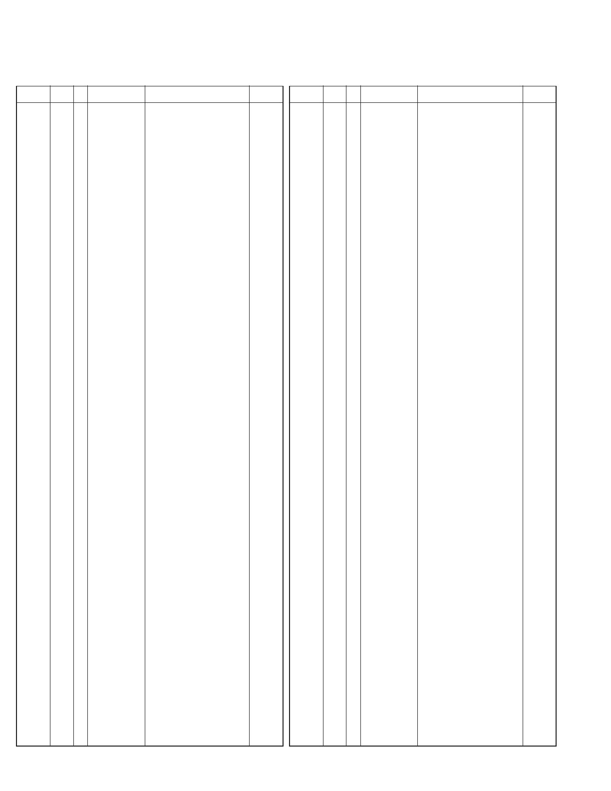
Kenwood M) User manual

Category
Telephones
Type
User manual

This manual is also suitable for

VHF FM TRANSCEIVER
TK-2160
© 2003-8 PRINTED IN JAPAN
B51-8652-00 (S) 1214
SERVICE MANUAL
Knob (CH-SELECTOR)
(K29-9280-13)
Knob (VOLUME)
(K29-9278-13)
Cabinet assy
(A02-3826-33)
Knob (PTT)
(K29-9279-03)
Antenna
(KRA-26: Option)
GENERAL .............................................................2
SYSTEM SET-UP .................................................2
OPERATING FEATURES .....................................3
REALIGNMENT....................................................4
DISASSEMBLY FOR REPAIR ..............................5
CIRCUIT DESCRIPTION .......................................7
INSTALLATION..................................................11
TERMINAL FUNCTION......................................12
SEMICONDUCTOR DATA .................................13
COMPONENTS DESCRIPTION .........................14
PARTS LIST........................................................15
EXPLODED VIEW...............................................23
PACKING ............................................................24
ADJUSTMENT ...................................................25
PC BOARD
TX-RX UNIT (X57-672X-XX) ........................30
SCHEMATIC DIAGRAM.....................................34
BLOCK DIAGRAM..............................................38
LEVEL DIAGRAM...............................................40
KSC-30................................................................41
SPECIFICATIONS............................BACK COVER
CONTENTS
Does not come with antenna.
Antenna is available as an option.
TK-2160
2
GENERAL / SYSTEM SET-UP
INTRODUCTION
SCOPE OF THIS MANUAL
This manual is intended for use by experienced technicians
familiar with similar types of commercial grade communications
equipment. It contains all required service information for the
equipment and is current as of the publication date. Changes
which may occur after publication are covered by either Service
Bulletins or Manual Revisions. These are issued as required.
ORDERING REPLACEMENT PARTS
When ordering replacement parts or equipment information,
the full part identification number should be included. This
applies to all parts, components, kits, or chassis. If the part
number is not known, include the chassis or kit number of
which it is a part, and a sufficient description of the required
component for proper identification.
PERSONAL SAFETY
The following precautions are recommended for personal
safety:
DO NOT transmit until all RF connectors are verified secure
and any open connectors are properly terminated.
SHUT OFF and DO NOT operate this equipment near
electrical blasting caps or in an explosive atmosphere.
This equipment should be serviced by a qualified technician
only.
SERVICE
This radio is designed for easy servicing. Refer to the
schematic diagrams, printed circuit board views, and alignment
procedures contained within.
SYSTEM SET-UP
Merchandise received
License and frequency allocated by FCC
Choose the type of transceiver
Transceiver programming
Delivery
Are you using the speaker microphone?
A personal computer (IBM PC or compatible), programming
interface (KPG-22), and programming software (KPG-82D)
are required for programming.
(The frequency, TX power HI/LOW, and signalling data are programmed
for the transceiver.)
YES
NO
KMC-17 or KMC-21
Speaker microphone
(Option)
Are you using the optional antenna?
YES
NO
KRA-22 or KRA-26
Optional antenna
TX/RX 136~174
5.0W
TK-2160 (K,M)
Frequency range (MHz) RF power Type
Unit
Model
TX-RX Unit Frequency range Remarks
& destination
TK-2160
K,M X57-6720-10 136~174MHz
IF1 : 49.95MHz
LOC : 50.4MHz
TK-2160
3
OPERATING FEATURES
1. Operation Features
Installing the (Optional) Antenna
Screw the antenna into the connector on
the top of the transceiver by holding the
antenna at its base and turning it clockwise
until secure.
Installing the Belt Clip
Note: When first installing the belt clip, you must remove the
battery pack from the rear of the transceiver.
1 Remove the two screws from the
rear of the transceiver, then remove
the small, plastic black covering that
was held in place.
2 Insert the belt clip mount into the
space on the rear of the transceiver.
3 Using the 2 screws, affix the belt
clip in place.
Note: Do not dispose of the plastic
black covering! If you remove
the belt clip, replace the covering
into the space on the rear of the
transceiver. Either this covering
or the belt clip must be in place,
otherwise the battery pack may
not remain installed properly.
Installing the Cover over the
Speaker/ Microphone Jacks
Note: When installing the speaker/
microphone jack cover, you must
remove the battery pack from the
rear of the transceiver.
If you are not using a speaker/
microphone, install the cover over the
speaker/ microphone jacks using the
supplied screw.
Note: To lift the cover after it has been installed, use a piece
of hardened plastic or metal, such as a small screwdriver.
Lift the cover by its tab, beside the screwhole, taking
care not to damage the cover.
Installing the (Optional) Speaker/ Microphone
Note: When installing the optional
speaker/ microphone and its
locking bracket, you must
remove the battery pack from
the rear of the transceiver.
1 Insert the speaker/ microphone
plugs into the speaker/ microphone
jacks.
2 Attach the locking bracket using the supplied screw.
Note: To lift the locking bracket after it has been installed,
use a piece of hardened plastic or metal, such as a small
screwdriver. Lift the bracket by its tab, beside the
screwhole, taking care not to damage the bracket.
GETTING ACQUAINTED
The transceiver is shown with the optional KNB-24L battery
pack.
qq
qq
q LED indicator
Lights red while transmitting. Lights green while receiving.
Flashes orange while receiving a 2-Tone, DTMF, or
FleetSync signal that matches the one set up in your
transceiver. If programmed by your dealer, flashes red when
the battery power is low while transmitting.
w Channel Switch
Rotate to select a channel from 1 to 16.
e Power switch/ Volume control
Turn clockwise to switch ON the transceiver. Rotate to
adjust the volume. To switch OFF the transceiver, turn
counterclockwise fully.
r AUX key
This is a PF (Programmable Function) key. Press it to activate
its auxiliary function (page 4). The default setting for this
key is None.
t PTT (Push-to-Talk) switch
Press this switch, then speak into the microphone to call a
station.
y Side 1 key
This is a PF (Programmable Function) key. Press it to activate
its auxiliary function (page 4). The default setting for this
key is None.
u Side 2 key
This is a PF (Programmable Function) key. Press it to activate
its auxiliary function (page 4). The default setting for this
key is Squelch Off Momentary. Press each key to activate
its auxiliary function.
i SP/MIC jacks
Connect an optional speaker/ microphone here.
Antenna
Microphone Speaker
4
1 2 3
5
8
6
7
TK-2160
4
OPERATING FEATURES /
REALIGNMENT
Programmable Auxiliary Functions
The AUX, Side 1, and Side 2 keys can be programmed
with the auxiliary functions listed below:
2-Tone Encode
Emergency
1
•Monitor Momentary
Monitor Toggle
None
RF Power Low
•Scan
Scan Temporary Delete
Scrambler
Squelch Off Momentary
Squelch Off Toggle
1
This function can be programmed only on the AUX key.
2. How to Enter Each Mode
Mode Operation
User mode Power ON
PC mode Received commands from PC
1. Modes
Mode Function
User mode For normal use.
PC mode Used for communication between the
radio and PC (IBM compatible).
Data programming Used to read and write frequency data
mode
and other features to and from the radio.
PC test mode Used to check the radio using the PC.
This feature is included in the KPG-
82D.
User mode
PC mode
PC test mode
Data programming
mode
PC tuning mode
REALIGNMENT
3.PC Mode
3-1. Preface
The TK-2160 transceiver is programmed using a personal
computer, a programming interface (KPG-22) and programming
software (KPG-82D).
The programming software can be used with an IBM PC
or compatible. Figure 1 shows the setup of an IBM PC for
programming.
3-2. Connection procedure
1. Connect the TK-2160 to the personal computer with the
interface cable.
2. When the POWER is switched on, user mode can be
entered immediately. When the PC sends a command,
the radio enters PC mode.
When data is transmitting from the transceiver, the red
LED lights.
When data is received by the transceiver, the green LED
lights.
Notes:
The data stored in the personal computer must match the
model type when it is written into the EEPROM.
Change the TK-2160 to PC mode, then attach the interface
cable.
3-3. KPG-22 description
(PC programming interface cable: Option)
The KPG-22 is required to interface the TK-2160 with the
computer. It has a circuit in its D-subconnector (25-pin) case
that converts the RS-232C logic level to the TTL level.
The KPG-22 connects the SP/MIC connector of the TK-2160
to the computer’s RS-232C serial port.
3-4. Programming software description
KPG-82D is the programming software for TK-2160
supplied on a CD-ROM. This software runs under Windows
98, ME, Windows 2000 or XP on an IBM-PC or compatible
machine.
The data can be input to or read from TK-2160 and edited
on the screen. The programmed or edited data can be printed
out. It is also possible to tune the transceiver.
Tuning cable
(E30-3216-05)
RF Power meter
or SSG
Gray +
Gray/Black
1.5D-XV Lead wire +
1.5D-XV Shield wire
}
}
SP
MIC
KPG-22
KPG-82D
IBM-PC
Fig. 1
TK-2160
5
DISASSEMBLY FOR REPAIR
/
/
,
Packing
1. Separating the case assembly from the chassis.
1. Remove the volume knob
z
.
2. Remove the two screws
x
.
3. Lift the chassis
c
,
and remove it from the case assembly.
Note: After separating the case assembly from the chassis,
remove the channel knob.
2. Separating the chassis from the TX/RX unit.
1. Remove the two screws
v
fixing the TX/RX unit B/2.
2. Remove the twelve screws
b
and two screws
n
fixing
the TX/RX unit A/2.
3. Remove the solder from the antenna terminal using a
soldering iron
m
, then lift the unit off.
z
x
x
c
Channel knob
m
,
.
v
v
b
b
b
b
b
b
b
n
TX/RX UNIT B/2
TX/RX UNIT A/2
3. How to remove the battery terminal block.
1. Remove the two screws /, then pull out the back cover .
2. Remove the screw
.
Note: To remove the TX/RX unit B/2, remove the solder using
a soldering iron
.
.
Note: The two screws
n
of TX/RX unit A/2 are fixing the
battery terminal block
,
.
TK-2160
6
Assembling
•Installation of battery terminal block and
packing
Install them so that no distortion or deformation occurs.
•Installation of speakers and cushion, and wire
styling of speakers
Install the speakers so that they do not protrude from the
cushion. Perform the wire styling of speakers as shown in a
photograph.
Attaching the cushion
Attach the cushion as shown in Fig. 1.
Note: Cushion must not cover the screws A,B and C.
DISASSEMBLY FOR REPAIR
Install the cushion
according to the
guide.
•Installation of chassis and cabinet assy
Wire Styling
B
A
C
Fig. 1
Take screw B and
MIC edge as reference
line when sticking.
G13-2018-04
Stick between screw
A and B.
G13-2017-04
G13-2020-04
Do not press this area, top
packing easily deform.
Second, press down the Chassis to the
cabinet assy as shown in the diagram.
Good Condition NG Condition
After mount, packing
should be in this
condition.
Packing deform.
Packing protruded out.
Note:
Take care that the packing does not protrude from the
chassis or case.
Replace the protruded or deformed packing with a new one.
First, mount the set to the cabinet assy.
TK-2160
7
5) Audio Amplifier Circuit
The demodulated signal from IC401 is amplified by IC602,
and goes to AF amplifier through IC601.
The signal then goes through an AF volume control
(VR801), and is routed to an audio power amplifier (IC605)
where it is amplified and output to the speaker.
Fig. 3 Wide/Narrow switching circuit
CIRCUIT DESCRIPTION
1. Frequency Configuration
The receiver utilizes double conversion. The first IF is 49.95
MHz and the second IF is 450 kHz. The first local oscillator
signal is supplied from the PLL circuit.
The PLL circuit in the transmitter generates the necessary
frequencies. Fig. 1 shows the frequencies.
Fig. 1 Frequency configuration
1) Front End (RF AMP)
The signal coming from the antenna passes through the
transmit/receive switching diode circuit, (D204,D206,D208
and D212) passes through a BPF (L411 and L412), and is
amplified by the RF amplifier (Q404).
The resulting signal passes through a BPF (L407 and L409)
and goes to the mixer. These BPFs are adjusted by variable
capacitors (D402,D403,D404 and D405). The input voltage
to the variable capacitor is regulated by voltage output from
the microprocessor (IC805).
2) First Mixer
The signal from the front end is mixed with the first local
oscillator signal generated in the PLL circuit by Q403 to
produce a first IF frequency of 49.95 MHz.
The resulting signal passes through the XF401 MCF to cut
the adjacent spurious and provide the opitimun
characteristics, such as adjacent frequency selectivity.
Fig. 2 Receiver section
2. Receiver
The frequency configuration of the receiver is shown in Fig. 2.
3) IF Amplifier Circuit
The first IF signal is passed through a four-pole monolithic
crystal filter (XF401) to remove the adjacent channel signal.
The filtered first IF signal is amplified by the first IF amplifier
(Q402) and then applied to the lF system IC (IC401). The
IF system IC provides a second mixer, second local
oscillator, limiting amplifier, quadrature detector and RSSI
(Received Signal Strength Indicator). The second mixer
mixes the first IF signal with the 50.4MHz of the second
local oscillator output (TCXO X1) and produces the second
IF signal of 450kHz.
The second IF signal is passed through the ceramic filter
(CF401) to remove the adjacent channel signal. The filtered
second IF signal is amplified by the limiting amplifier and
demodulated by the quadrature detector with the ceramic
discriminator (CD401). The demodulated signal is routed
to the audio circuit.
4) Wide/Narrow Switching Circuit
Narrow and Wide settings can be made for each channel
by switching the demodulation level.
The WIDE (high level) and NARROW (low level) data is
output from IC805, pin 54.
When a WIDE (high level) data is received, Q401 turn off.
When a NARROW (low level) data is received, Q401 turn on.
Q401 turns on/off with the Wide/Narrow data and the
IC401 detector output level is switched to maintain a
constant output level during wide or narrow signals.
SP
BPF
IC602
AF Amp
IC601
IC605
AF PA
IC401
IF,MIX,DET
ANT
AQUA
CF401
TCXO
TUNE
Q4
X3 multiply
TUNE
ANT SW
BPF
MCF
1st Local
RF AMP
Q404
MIXER
Q403
XF401
IF AMP
Q402
AF VOL
X1
16.8MHz
2nd Local
Q401
H : Wide
L : Narrow
C409
W/N
R408
R409
CD401
IFO
QUAD
IC401
FM IF SYSTEM
5R
AFOUT
Q402
SP
TX: 136 ~ 174MHz (K,M)
PLL
VCO
IF SYSTEM
ANT
TCXO
X3 multiply
49.95MHz
MCF
AF
AMP
MIC
MIC
AMP
TX
AMP
RF
AMP
50.4MHz
CF
450kHz
RX: 185.95 ~ 233.95MHz
(K,M)
TX/RX: 136 ~ 174MHz (K,M)
16.8MHz
RF
AMP
ANT SW
TK-2160
8
RECEIVE SIGNALING
RECEIVE SIGNALING
SP
Q608
SW
IF Amp
FM IF IC401
IC602
IF Amp
IC601
IC605
AF PA
IC805
IC603
BPF & COMPALATER
Q603,604,607
SW
QT/DQT
2-TONE
DTMF
CLK,DATA,
STD,LOADN
SIGNAL
SP MUTE
HSDI
LSDI
AN SQL
CPU
AQUA
CIRCUIT DESCRIPTION
Fig. 5 AF amplifier and squelch
6) Tone Volume Fixed Circuit
This function generates a TONE signal sound even if the
AF volume of the transceiver is the minimum.
A TONE signal is sent through Q602 to the AF amplifier
when, in the FPU, “TONE Volume Fixed” is set to ON.
7) Squelch
Part of the AF signal from the IC enters the FM IC (IC401)
again, and the noise component is amplified and rectified
by a filter and an amplifier to produce a DC voltage
corresponding to the noise level.
The DC signal from the FM IC goes to the analog port of
the microprocessor (IC805). IC805 determines whether
to output sounds from the speaker by checking whether
the input voltage is higher or lower than the preset value.
To output sounds from the speaker, IC805 sends a high
signal to the SP MUTE line and turns IC605 on through
Q603,Q604,Q607 and Q608. (See Fig. 5)
8) Receive Signalling
(1) QT/DQT
The output signal from IF IC(IC401) enters the
microprocessor(IC805) through IC601. IC805 determines
whether the QT or DQT matches the preset value, and
controls the SP MUTE and the speaker output sounds
according to the squelch results.
(2) 2-TONE
Part of the received AF signal output from the AF amplifier
IC602, and then passes through an audio processor
(IC601), goes to the other AF amplifier IC603, is compared,
and then goes to IC805. IC805 checks whether 2-TONE
data is necessary. If it matches, IC805 carries out a
specified operation, such as turning the speaker on. (See
Fig. 5)
(4) DTMF
The DTMF input signal from the IF IC (IC401) is amplified
by IC602 and goes to IC601. The decoded information is
then processed by the CPU.
3. PLL Frequency Synthesizer
The PLL circuit generates the first local oscillator signal for
reception and the RF signal for transmission.
1) PLL
The frequency step of the PLL circuit is K:2.5,5,6.25 or
7.5kHz, M:6 or 6.25kHz.
A 16.8MHz reference oscillator signal is divided at IC1 by a
fixed counter to produce an oscillator (VCO) output signal
which is buffer amplified by Q9 then divided in IC1 by a
dual-module programmable counter. The divided signal is
compared in phase with the 5 or 6.25kHz reference signal
from the phase comparator in IC1. The output signal from
the phase comparator is filtered through a low-pass filter
and passed to the VCO to control the oscillator frequency.
(See Fig. 6)
2) VCO
The operating frequency is generated by Q6 in transmit
mode and Q5 in receive mode. The oscillator frequency is
controlled by applying the VCO control voltage, obtained
from the phase comparator, to the varactor diodes
(D3,D5,D7 and D8 in transmit mode and D4,D6,D9 and D10
in receive mode). The RX pin is set high in receive mode
causing Q8 and Q12 to turn Q6 off and Q5 on.
The TX pin is set high in transmit mode. The outputs from
Q5 and Q6 are amplified by Q9 and sent to the RF amplifiers.
Fig. 4 Tone volume fixed circuit
IC805
CPU
BEEP
BEEPSW
TONE VOL FIXED
IC601
AQUA
VOL
IC605
TA7368F
Q602
Hi: ON
LOW: OFF
+
SP
SP-J
[VOL Position vs Output Level]
Output Level (mV)
Min
ON
OFF
25
500
Center Max
(3) MSK (Fleet Sync)
Fleet Sync utilizes 1200bps and 2400bps MSK signal is
output from pin 6 of IC601. And is routed to the VCO.
When encoding MSK, the microphone input signal is muted.
TK-2160
9
CIRCUIT DESCRIPTION
PLL DATA
X1
16.8MHz
REF OSC
1M
1N
PLL IC IC1
PHASE
COMPARATOR
CHARGE
PUMP
LPF
5kHz/6.25kHz
D3, 5, 7, 8
D4, 6, 9, 10
Q6
TX VCO
Q5
RX VCO
Q9
BUFF AMP
Q11
RF AMP
Q7
DOUBLER
Q8, 12
T/R SW
5kHz/6.25kHz
LPF
RX
TX
Fig. 6 PLL circuit
3) Unlock Detector
If a pulse signal appears at the LD pin of IC1, an unlock
condition occurs, and the DC voltage obtained from C19,R6
and Q1 causes the voltage applied to the microprocessor
to go high. When the microprocessor detects this condition,
the transmitter is disabled, ignoring the push-to-talk switch
input signal. (See Fig. 7)
Fig. 7 Unlock detector circuit
5C
R6
Q1
C19
R7
IC805
IC1
LD
UL
PLL IC
CPU
R16
4. Transmitter System
1) Microphone Amplifier
The signal from the microphone passes through the IC601.
When encoding DTMF, it is turned OFF for muting the
microphone input signal by IC601.
The signal passes through the Audio processor (IC601) for
the maximum deviation adjustment, and goes to the VCXO
modulation input.
Fig. 8 Microphone amplifier
Fig. 9 Drive and final amplifier and APC circuit
3) APC Circuit
The APC circuit always monitors the current flowing through
the RF power amplifier (Q211) and keeps a constant current.
The voltage drop at R264, R265 and R270 is caused by the
current flowing through the RF power amplifier and this
voltage is applied to the differential amplifier IC201(1/2).
IC201(2/2) compares the output voltage of IC201(1/2) with
the reference voltage from IC805. The output of IC201(2/2)
controls the VG of the RF power amplifier, drive amplifier
and pre-drive amplifier to make both voltages the same.
The change of power high/low is carried out by the change
of the reference voltage.
4) Encode Signalling
(1) QT/DQT
QT,DQT data of the LSDTCXO Line is output from pin 22 of
the CPU. The signal passes through a low-pass CR filter
and goes to the TCXO(X1).
The QT,DQT data of the LSDVCO Line is output from pin
2) Drive and Final Amplifier
The signal from the T/R switch (D201 is on) is amplified by
the drive amplifier (Q207) to 50mW.
The output of the drive amplifier is amplified by the RF power
amplifier (Q211) to 5.0W (1W when the power is low). The
RF power amplifier consists of two MOS FET stages. The
output of the RF power amplifier is then passed through
the harmonic filter (LPF) and antenna switch (D204 and
D206) and applied to the antenna terminal.
From
T/R SW
(D201)
DRIVE
AMP
RF
POWER AMP
LPF
ANT
SW
D204
D206
AN
T
VGVG
Q207 Q211
Pre-DRIVE
AMP
Q206
VDD
VG
R264
R265
R270
+B
IC201
(2/2)
IC201
(1/2)
PCTV
(IC805)
IC601
IC805
LPF
DTMF/2 TONE
LSDTCXO
LSDVCO
CPU
AGC
VCO
MIC
X1
TCXO
LPF
IC606
BUFFER
LPF
AQUA
TK-2160
10
2) Memory Circuit
Memory circuit consists of the CPU (IC805) and an EEPROM
(IC804). An EEPROM has a capacity of 64k bits that contains
the transceiver control program for the CPU and data such
as transceiver channels and operating features.
3) Low Battery Warning
The battery voltage is checked using by the microprocessor.
The transceiver generates a warning tone when it falls below
the warning voltage shown in the table.
(1)The red LED blinks when the battery voltage falls below
the voltage (1) shown in the table during transmission.
(2)The red LED blinks when the battery voltage falls below
the voltage (2) shown in the table during transmission.
Note:
The transceiver checks the battery voltage during reception
even when, in the FPU, the Battery Warning status function
is set to “On TX” (default setting).
However, the LED does not blink during reception. During
transmission, the LED blinks to generate the warning tone
of a low battery voltage.
(3)The transceiver immediately stops transmission when
the battery voltage falls below the voltage (3) shown in
the table. A message tone beeps while the PTT switch
is released.
CIRCUIT DESCRIPTION
6. Control Circuit
The control circuit consists of a microprocessor (IC805) and
its peripheral circuits. It controls the TX-RX unit. IC805 mainly
performs the following:
(1) Switching between transmission and reception by the
PTT signal input.
(2) Reading system, group, frequency, and program data
from the memory circuit.
(3) Sending frequency program data to the PLL.
(4) Controlling squelch on/off by the DC voltage from the
squelch circuit.
(5)Controlling the audio mute circuit by the decode data input.
(6) Transmitting tone and encode data.
1) Frequency Shift Circuit
The microprocessor (IC805) operates at a clock of
7.3728MHz. This oscillator has a circuit that shifts the
frequency by BEAT SHIFT SW (Q810).
A beat sound may be able to be evaded from generation if
“Beat Shift” is set to ON when it is generated in the internal
spurious transmission modulated sound of a transceiver.
20 of the CPU. The signal passes through a low pass CR
filter, mixes with the audio signal, and goes to the VCO
modulation input. TX deviation is adjusted by the CPU.
(2) DTMF/2 TONE
High-speed data is output from pin 2 of the CPU. The signal
passes through a low-pass CR filter, and provides a TX and
SP out tone, and is then applied to the audio processor
(IC601). The signal is mixed with the audio signal and goes
to the VCO.
TX deviation is adjusted by the CPU.
(3) MSK (Fleet Sync)
The MSK input signal from the IF IC is amplified by IC602
(1/2) and goes to pin 31 of IC 601. The signal is demodulated
by MSK demodulator in IC 601. The demodulated data goes
to the CPU for processing.
5. Power Supply
There are 3.5V power supply for PLL circuit and five 5V
power supplies for the microprocessor: 5M,5MS,5C,5R, and
5T. 5M is always output while the power is on. 5M is always
output, but turns off when the power is turned off to prevent
malfunction of the microprocessor.
5C is a common 5V and is output when SAVE is not set to
OFF.
5R is 5V for reception and output during reception.
5T is 5V for transmission and output during transmission.
X801C834
XOUT
IC805
Q810
Hi: OFF
LOW: ON
BSHIFT
Fig. 10 Frequency shift circuit
Fig. 11 Memory circuit
IC805
CPU
IC804
EEPROM
Battery Case Li-ion Battery Ni-Cd Battery Ni-MH Battery
(1) 6.2[V] 6.5[V] 6.2[V] 6.2[V]
(2) 7.6[V] 7.1[V] 6.8[V] 7.0[V]
(3) 5.9[V] 6.2[V] 5.9[V] 5.9[V]
SB
R833
R834
88
IC805
CPU
Fig. 12 Low battery warning
TK-2160
11
4) Battery Type Detection
The transceiver automatically detects the battery type,
measuring the resistance between the S-terminal and +
terminal on the battery pack and changes the supplied
voltage to the S-tarminal as below. The microprocessor then
detects the battery type.
7. Control System
Keys and channel selector circuit.
The signal from the keys and channel selector are directly
input to the microprocessor, as shown in fig. 13.
Fig. 13 Control system
Channel selector
CPU
IC805
SIDE 2
EN4
EN3
EN2
EN1
67
68
69
70
PTT
PTT
SW
SIDE 1
34
74
75
76
AUXSW
AUX SW
SW1
SW2
CIRCUIT DESCRIPTION / INSTALLATION
Resistor value Battery type Input voltage of S-terminal
1.8M Li-ion 0.3~1.3V
560k Ni-Cd 1.3~2.6V
220k Ni-MH 2.6~5.0V
OPEN Battery case 0~0.3V
INSTALLATION
1. Optional Board
Remove the TX/RX unit from the radio before installing the
optional board in the radio.
The procedure for removing the TX/RX unit is described in
the DISASSEMBLY FOR REPAIR section in the Service
Manual.
Install the optional board on the back of the TX/RX unit.
For details on installation of the optional board, refer to
Installation Information supplied with the optional board.
When installing the optional board, also refer to the chart in
TERMINAL FUNCTION section (page 12) given in the Service
Manual.
Note: To install and use the Scrambler Board, remove “R601”
and “R647” from the front of the TX/RX unit.
R647 R601
R601
R607
R608
R609
R610
R613
R615
R616
R
617
R618
R621
R622
R623
R624
R625
R626
R627
R628
R629
R631
R632
R633
R634
R636
R640
R641
R835
R642
R836
C607
R643
C608
C609
R839
R647
R840
C610
C613
C614
C618
C619
C621
C622
C625
R855
R856
C628
C630
C1
C631
C632
C633
C634
C4
C635
C636
C637
C640
C641
C642
C643
C645
C646
C648
C846
C847
R695
IC601
CP803
4
CP808
CP809
CP810
CP812
CP813
CP814
R1
R2
R3
C
606
L804
L806
R696
C627
C3
19
10
16
1725
26
32
+
75
76
51
50
CE
VCC
++
+
TX-RX UNIT (X57-6720-10)
Component side view
TK-2160
12
TERMINAL FUNCTION
CN801
1 GND GND Vss
2SB Switched B Output Voltage/7mA load DC (Battery terminal) ±0.5V
3A3 AUX3 Load >100k (Low) Vss ~ 0.4V (High) Vdd-0.8V ~ Vdd
4 TXAFI Transmit AF input Input sensitivity/Impedance (1kHz std. dev.) 280±50mVrms @22k Load
5A2 AUX2 Load >100k (Low) Vss ~ 0.4V (High) Vdd-0.8V ~ Vdd
6A6 AUX6 Load >100k (Low) Vss ~ 0.4V (High) Vdd-0.8V ~ Vdd
7A1 AUX1 Load >100k (Low) Vss ~ 0.4V (High) Vdd-0.8V ~ Vdd
8A5 AUX5 Load >100k (Low) Vss ~ 0.4V (High) Vdd-0.8V ~ Vdd
9A4 AUX4 Load >100k (Low) Vss ~ 0.4V (High) Vdd-0.8V ~ Vdd
10 NC Non connection Non connection
11 5C DC 5V Output Voltage/10mA load 5.0±0.5V
12 DEO Discriminator signal output Output voltage/Impedance (1kHz std. mod.) 280±50mVrms @2.2k Load
13 TXAFI Transmit AF input Input sensitivity/Impedance (1kHz std. dev.) 280±50mVrms @22k Load
14 DEO Discriminator signal output Output voltage/Impedance (1kHz std. mod.) 280±50mVrms @2.2k Load
15 NC Non connection Non connection
16 ALT Sidetone input
Input sensitivity/Impedance
7 ±3mVrms @22k Load
(1kHz rated AF power/Vol. MAX)
17 NC Non connection Non connection
18 NC Non connection Non connection
19 NC Non connection Non connection
20 GND GND Vss
Pin
Designation
Function Condition Value
No.
Solder point connection
MIC_I Mic input Input sensitivity/Impedance (1kHz std. dev.) 7±3mVrms @22k Load
MIC_O Mic o utput
Output voltage/Impedance (1kHz 15mVrms mic input) 2.6±1.0mVrms @2.2k Load
Output voltage/Impedance (1kHz 100mVrms mic input) 90±20mVrms @100k Load
RA_I Receiver AF input Input sensitivity/Impedance (1kHz rated AF power/Vol. MAX) 75±20mVrms @22k Load
RA_O Receiver AF output
Output voltage/Impedance (1kHz std. mod.) 150±50mVrms @2.2k Load
Output voltage/Impedance (1kHz system mod.) 290±50mVrms @100k Load
A1 AUX1 Load >100k (Low) Vss ~ 0.4V (High) Vdd-0.8V ~ Vdd
A2 AUX2 Load >100k (Low) Vss ~ 0.4V (High) Vdd-0.8V ~ Vdd
A3 AUX3 Load >100k (Low) Vss ~ 0.4V (High) Vdd-0.8V ~ Vdd
A4 AUX4 Load >100k (Low) Vss ~ 0.4V (High) Vdd-0.8V ~ Vdd
A5 AUX5 Load >100k (Low) Vss ~ 0.4V (High) Vdd-0.8V ~ Vdd
A6 AUX6 Load >100k (Low) Vss ~ 0.4V (High) Vdd-0.8V ~ Vdd
SB Switched B Output Voltage/7mA load DC (Battery terminal) ±0.5V
GND GND Vss
5C DC 5V Output Voltage/10mA load 5.0±0.5V
TXAFI Transmit AF input Input sensitivity/Impedance (1kHz std. dev.) 280±50mVrms @22k Load
DEO Discriminator signal output Output voltage/Impedance (1kHz std. mod.) 280±50mVrms @2.2k Load
LSDFO Received sub-tone output Output voltage/Impedance (150Hz 15% mod.) 180±50mVrms @2.2k Load
ALT Sidetone input Input sensitivity/Impedance (1kHz rated AF power/Vol. MAX) 7±3mVrms @22k Load
Designation
Function Condition Value
TK-2160
13
Microprocessor : M30622MCA7G7GP (TX-RX UNIT : IC805)
Pin function
1 PCTV O APC/BPF control data output.
2 DTMF O DTMF, 2TONE.
3 HSDI I High speed data input (2TONE).
4 EEPDAT I/O EEPROM data input/output.
5 EEPCLK O EEPROM Clock
6 BYTE I GND.
7 CNVSS I GND.
8 AUX5 O Option Board 5
9 AUX6 O Option Board 6
10 RESET I CPU reset.
11 XOUT O CPU clock.
12 VSS - GND.
13 XIN I CPU clock.
14 VCC - +5V.
15 NC I NC
16 INT I Battery voltage monitor input Low battery : L
17 RDF/FD I Base Band IC Data input
18
TCLK/
I Base Band IC Data input
DTRDI
19 NC - NC
20 LSDVCO O Low speed data output (VCO).
21 NC I NC
22
LSDTCXO
O Low speed data output (TCXO).
23 NC I NC
24 BEEP O Beep output.
25 OPTDET I Option detect input
26 NC - NC
27 NC - NC
28 NC - NC
29 AUX4 O Option board port 4
30 AUX2 I/O Option board port 2
31 NC - NC
32 NC - NC
33 TXD I/O Serial data.
34 PTT/RXD I PTT on : L/Serial data.
35 STD I Base Band IC Data input
36 BBDIR O Base Band IC Data output
37 BBCLK O Base Band IC clock output
38 BBDI/O I/O Base Band IC Data input/output
39 NC - NC
40
TDATA/
O Base Band IC Data output
DTRCLK
41
DTRLOADN
O Base Band IC Data output
42 AUX3 O Option board port 3
43 AUX1 O Option board port 1
44 NC - NC
45 NC - NC
46 DSW O APC voltage discharge Switch
47
BEEPSW
O Beep switch.
48 AFCOUT O AF amp power supply control
49 AFMUTE O RX audio mute
50 NC - NC
51 TX O TX VCO power supply switch TX:L
52 RX O RX VCO power supply switch RX:L
Pin Port
I/O Function
No. Name
Pin Port
I/O Function
No. Name
53 BSHIFT O Beet shift switch.
54 W/N O W/N switch Wide:H
55 NC - NC
56 APCSW O APC switch output.
57 SAVE O Battery save output.
58 5TC O 5T control output.
59 5RC O 5R control output.
60 VCC - +5V.
61 5MSC O 5M control output.
62 VSS - GND.
63 NC - NC
64 NC - NC
65 NC - NC
66 NC - NC
67 EN4 I CH selector input 4.
68 EN3 I CH selector input 3.
69 EN2 I CH selector input 2.
70 EN1 I CH selector input 1.
71 NC - NC
72 LEDTX O RED LED lights control output
73 LEDRX O GREEN LED lights control output
74 AUXSW I Key input (Emergency).
75 SIDE1 I Side key 1 input.
76 SIDE2 I Side key 2 input.
77 NC - NC
78 NC - NC
79 SIM1 I Destination select 1.
80 SIM2 I Destination select 2.
81 NC - NC
82 PLLUL I PLL unlock detect input. unlock : L
83 RFCLK O PLL clock output. Latch : L
84 RFDAT O PLL data output.
85 PS O PLL power save output.
86 PLLSTB O PLL strobe output.
87
BATTSEL
I Battery distinction input.
88 BATT I Battery voltage input.
89 VOX I VOX input.
90 RSSQL I Received signal strength indicator input.
91 ANSQL I Squelch level input.
92 LSDI I Low speed data input (QT/DQT).
93 THM I Thermistor input.
94 AVSS - GND.
95 NC - NC
96 VREF - +5V.
97 AVCC - +5V.
98 NC - NC
99 NC - NC
100 NC - NC
SEMICONDUCTOR DATA
TK-2160
14
COMPONENTS DESCRIPTION
IC1 IC PLL system
IC201 IC Comparator (APC)
IC401 IC FM IF system
IC601 IC Audio processor
IC602 IC AF AMP
IC603(1/2)
IC HSD AMP
IC603(2/2)
IC HSD AMP
IC604 IC VOX AMP
IC605 IC AF Power AMP
IC606 IC AF AMP
IC801 IC Voltage regulator / 5V
IC802 IC Voltage detector / Reset
IC803 IC Voltage detector / INT
IC804 IC EEPROM
IC805 IC Microprocessor
IC806 IC Flip Flop
Q1 Transistor Level shift
Q2 Transistor Level shift
Q3 Transistor Level shift
Q4 Transistor Tripler
Q5 FET VCO / RX
Q6 FET VCO / TX
Q7 Transistor Doubler
Q8 FET DC switch / TX VCO
Q9 Transistor RF Buffer AMP
Q10 Transistor Ripple filter
Q11 Transistor RF AMP
Q12 FET DC switch / RX VCO
Q206 FET Pre-drive AMP
Q207 FET TX Drive AMP
Q208 Transistor APC switch
Q209 FET APC switch
Q210 Transistor APC switch
Q211 FET TX Final AMP
Q212 FET APC switch
Q213 Transistor APC switch
Q400 FET W/N switch / TX
Q401 Transistor W/N switch / RX
Q402 Transistor IF AMP
Q403 FET Mixer
Q404 FET RF AMP
Q601 FET AF Mute
Q602 FET Beep switch
Q603 Transistor DC switch / SP Mute
Q604 Transistor DC switch
Q605 Transistor MIC AGC
Q606 Transistor MIC AGC
Q607 Transistor DC switch / SP Mute
Q608 FET SP Mute switch
Q801 Transistor 5T switch
Q802(1/2) FET 5TC switch
Q802(2/2) FET SAVE switch
Q803(1/2) Transistor AVR / 5C
Q803(2/2) Transistor AVR / 5T
Q804 Transistor 5C switch
Q805(1/2) Transistor LED switch / Green
Q805(2/2) Transistor LED switch / Red
Q806 Transistor AVR / PLLB
Q807 Transistor PLLB switch
Q808 Transistor 5MS switch
Q809 Transistor 5R switch
Q810 FET Beet shift switch
D2 diode Shift switch
D3
Variable
Frequency control / TX VCO
capacitance diode
D4
Variable
Frequency control / RX VCO
capacitance diode
D5
Variable
Frequency control / TX VCO
capacitance diode
D6
Variable
Frequency control / RX VCO
capacitance diode
D7
Variable
Frequency control / TX VCO
capacitance diode
D8
Variable
Frequency control / TX VCO
capacitance diode
D9
Variable
Frequency control / RX VCO
capacitance diode
D10
Variable
Frequency control / RX VCO
capacitance diode
D11 Diode Shift switch
D12
Variable
Modulator
capacitance diode
D13 Diode Current steering
D14 Diode Shift switch
D201 Diode TX/RX RF switch
D203 Zener diode APC protect
D204 Diode ANT switch
D206 Diode ANT switch
D208 Diode ANT switch
D212 Diode ANT switch
D401 Diode TX/RX RF switch
D402
Variable
RF BPF tuning
capacitance diode
D403
Variable
RF BPF tuning
capacitance diode
D404
Variable
RF BPF tuning
capacitance diode
D405
Variable
RF BPF tuning
capacitance diode
D603 Diode Limitter
D604 Diode Detector
D605 Diode Detector
D606 Diode Detector
D801 Diode 5M protector
D802 LED LED / Red
D803 LED LED / Green
D805 Diode Reverse protection
Ref. No.
Use/Function
Operation/Condition
TX-RX UNIT (X57-672X-XX)
Ref. No.
Use/Function
Operation/Condition
TK-2160
15
PARTS LIST
CAPACITORS
1 = Type ... ceramic, electrolytic, etc.
2 = Shape ... round, square, ect.
3 = Temp. coefficient
4 = Voltage rating
5 = Value
6 = Tolerance
Color*
CC45
Capacitor value
010 = 1pF
100 = 10pF
101 = 100pF
102 = 1000pF = 0.001µF
103 = 0.01µF
22
Multiplier
2nd number
1st number
0 = 22pF
CC 45
TH 1H J220
1
2
3
4
6
5
Temperature coefficient
Tolerance (More than 10pF)
Voltage rating
Chip capacitors
1
1st Word
Color*
Code
DGJKMXZP
No code
LCPRSTU
Black Red Orange Yellow Green Blue Violet
0 -80 -150 -220
+ 40
- 40
+ 80
- 20
+ 100
-0
-330 -470 -750
C
(%)
ppm/
0.25 0.5 2 5 10 20
More than 10µF -10 +50
Less than 4.7µF-10 +75
2nd Word HG
Example : CC45TH = -470
JKL
ppm/
30 60
0.1 0.25 0.5 1 2
120 250 500
60ppm/
Gode
CDFGB
(pF)
(Less than 10pF)
1st word
2nd word
A
0
2.0
2.5
3.15
20
25
31.5
200
250
315
2000
2500
3150
1.0
1.25
1.6
10
12.5
16
100
125
160
1000
1250
1600
1
2
3
BCDEF
4.0
40
400
4000
G
5.0
50
500
5000
H
6.3
63
630
6300
J
8.0
80
800
8000
K
-
35
-
-
V
(EX) C C 7 3 F S L 1 H
000
J
Refer to the table above.
1 = Type
2 = Shape
5 = Voltage rating
4 = Temp. coefficient
3 = Dimension
6 = Value
7 = Tolerance
7654321
(EX) C K 7 3 F F 1 H
000
Z
7654321
(Chip)(CH,RH<UJ,SL)
(Chip)(B,F)
Chip resistor (Carbon)
(EX) R K 7 3 E B 2 B
000
J
7654321
RESISTORS
(Chip)(B,F)
Carbon resistor (Nomal type)
(EX) R D 1 4 B B
2C
000
J
7654321
1 = Type
2 = Shape
5 = Rating wattage
4 = Temp. coefficient
3 = Dimension
6 = Value
7 = Tolerance
Dimension code L W T
Empty
A
B
C
D
E
F
G
H
L
W
T
0.5
5.0
0.4
3.2
0.3
2.0
0.2
1.25
0.2
1.6
0.2
1.25
0.2
0.8
0.05
0.5
0.05
0.5
0.3
2.5
0.5
5.6
0.5
4.5
0.5
4.5
0.5
4.5
0.2
3.0
0.3
2.0
0.2
1.6
0.05
1.0
0.4
3.2
Less than 2.0
Less than 2.0
Less than 2.0
Less than 1.25
Less than 1.5
Less than 1.25
Less than 1.25
Less than 1.0
Dimension (Chip capacitors)
Dimension (Chip resistor)
Rating wattage
Dimension
Dimension code L W T
E
F
G
H
0.2
1.6
0.2
1.25
0.2
0.8
0.05
0.5
0.1
0.5
0.05
0.35
0.2
3.2
0.3
2.0
0.2
1.6
0.05
1.0
1.0
1.0
Code
2C
2H
2E
Wattage
1/6W
1/2W
1/4W
Code
1J
2B
2A
Wattage
1/16W
1/8W
1/10W
Code
3A
3D
Wattage
1W
2W
TK-2160
PARTS LIST
16
New Parts. indicates safety critical components.
Parts without Parts No. are not supplied.
Les articles non mentionnes dans le Parts No. ne sont pas fournis.
Teile ohne Parts No. werden nicht geliefert.
L:
Scandinavia
K:
USA
P:
Canada
Y:
PX (Far East, Hawaii)
T:
England
E:
Europe
Y:
AAFES (Europe)
X:
Australia
M:
Other Areas
Parts No. Description
Address
New
parts
Destination Destination
TK-2160
Ref. No.
Parts No. Description
Address
New
parts
TK-2160 (Y50-578X-XX)
TX-RX UNIT (X57-672X-XX)
Ref. No.
11B A02-3826-33 CABINET ASSY
22B A10-4068-01 CHASSIS
33A A82-0054-02 REAR PANEL
43AB01-0694-03 ESCUTCHEON
52D B09-0676-03 CAP ACCESSORY
61C B62-1716-00 INSTRUCTION MANUAL K
61C B62-1747-00 INSTRUCTION MANUAL M
73B B72-2153-04 MODEL NAME PLATE
83A E04-0446-05 RF COAXIAL RECEPTACLE(SMA)
93B E37-1085-05 FLAT CABLE
10 2A E37-1101-05 SPEAKER WIRE(RED)
11 2A E37-1102-05 SPESKER WIRE(BLACK)
12 3A E72-0416-13 BATT TERMINAL BLOCK
13 G10-1315-04 FIBROUS SHEET(CABINET)
14 2B G11-4090-04 SHEET(FINAL FET)
15 3B G11-4254-04 SHEET(PTT)
16 3A G11-4287-04 SHEET(TERMINAL BLOCK)
17 3A G11-4289-04 SHEET(CHASSIS)
18 2B G13-2001-04 CUSHION(CHASSIS)
19 2B G13-2014-04 CUSHION(CHASSIS BOTTOM)
20 2B G13-2017-04 CUSHION
21 2B G13-2018-04 CUSHION
22 3A G13-2019-04 CUSHION
23 2B G13-2020-04 CUSHION
24 3A G53-1579-02 PACKING
25 2B G53-1580-03 PACKING(CHASSIS)
26 1B G53-1581-22 PACKING(SPEAKER)
27 3B G53-1582-03 PACKING(BATT TERMINAL BLOCK)
28 3C H12-3150-02 PACKING FIXTURE
29 H25-2345-04 PROTECTION BAG
30 1D H52-1981-02 ITEM CARTON CASE
31 2A J19-5454-03 HOLDER
32 2D J21-8464-04 HARDWARE FIXTURE ACCESSORY
33 2C J29-0701-05 HOOK ACCESSORY
34 3A J30-1275-04 SPACER(CH KNOB)
35 3A J30-1281-04 SPACER(CH KNOB)
36 J30-1283-04 SPACER
37 1A K29-9278-13 KNOB(VOLUME)
38 1B K29-9279-03 KNOB(PTT)
39 3A K29-9280-13 KNOB(CH SELECTOR)
A3AN14-0583-04 CIRCULAR NUT(CH)
B3A N14-0805-04 CIRCULAR NUT(VOLUME)
C3AN30-2604-46 PAN HEAD MACHINE SCREW
D3BN30-2612-46 PAN HEAD MACHINE SCREW
E 3A,3B N30-3006-45 PAN HEAD MACHINE SCREW
F2DN35-3004-45 BINDING HEAD MACHINE SCREW
G 3A,3B N78-2040-46 PAN HEAD TAPTITE SCREW
H 2A,2B N83-2005-46 PAN HEAD TAPTITE SCREW
40 2A R31-0650-05 VARIABLE RESISTOR
41 2A S60-0420-05 ROTARY SWITCH
42 1B T07-0369-05 SPEAKER
D802 B30-2156-05 LED(RED)
D803 B30-2157-05 LED(YELLOW)
C1 CK73GB1H822K CHIP C 8200PF K
C2 CK73GB1H102K CHIP C 1000PF K
C3 CK73GB1E123K CHIP C 0.012UF K
C4 CK73GB0J225K CHIP C 2.2UF K
C5 CK73GB1H102K CHIP C 1000PF K
C6 CK73GB1H103K CHIP C 0.010UF K
C7 CK73GB1H102K CHIP C 1000PF K
C8 CC73GCH1H100D CHIP C 10PF D
C9 CK73GB1H103K CHIP C 0.010UF K
C10 CC73GCH1H100D CHIP C 10PF D
C11-13 CC73GCH1H101J CHIP C 100PF J
C14 C92-0713-05 CHIP-TAN 10UF 6.3WV
C15 CK73GB1H102K CHIP C 1000PF K
C16 CC73GCH1H470J CHIP C 47PF J
C18,19 CK73GB1C104K CHIP C 0.10UF K
C22 CK73GB1C104K CHIP C 0.10UF K
C23 CK73GB0J225K CHIP C 2.2UF K
C24 C92-0713-05 CHIP-TAN 10UF 6.3WV
C25 CK73GB1H102K CHIP C 1000PF K
C27 CK73GB1H102K CHIP C 1000PF K
C28 CC73GCH1H560J CHIP C 56PF J
C30 CC73GCH1H220J CHIP C 22PF J
C31 CC73GCH1H560J CHIP C 56PF J
C32 C92-0002-05 CHIP-TAN 0.22UF 35WV
C33 CC73GCH1H470J CHIP C 47PF J
C34 CK73GB1H102K CHIP C 1000PF K
C35 CC73GCH1H680J CHIP C 68PF J
C36 C92-0560-05 CHIP-TAN 10UF 6.3WV
C37 CK73GB1H102K CHIP C 1000PF K
C38,39 C92-0504-05 CHIP-TAN 0.68UF 20WV
C40 CK73GB1H471K CHIP C 470PF K
C41 CK73GB1H103K CHIP C 0.010UF K
C42 CK73GB1H183K CHIP C 0.018UF K
C43 CK73GB1A105K CHIP C 1.0UF K
C44 CK73FB1A225K CHIP C 2.2UF K
C45 CC73GCH1H120J CHIP C 12PF J
C46 CC73GCH1H090B CHIP C 9.0PF B
C47 CC73GCH1H040B CHIP C 4.0PF B
C48 CK73HB1C103K CHIP C 0.010UF K
C49 CK73HB1H102K CHIP C 1000PF K
C50 CC73GCH1H120J CHIP C 12PF J
C52 CC73GCH1H050B CHIP C 5.0PF B
C53 CC73HCH1H560J CHIP C 56PF J
C54 CC73HCH1H220J CHIP C 22PF J
C55 CC73GCH1H050B CHIP C 5.0PF B
C56,57 CC73HCH1H270J CHIP C 27PF J
C58 CC73GCH1H150J CHIP C 15PF J
C59 CC73HCH1HR75C CHIP C 0.75PF C
C60 CC73GCH1H070B CHIP C 7.0PF B
C61 CC73HCH1H070B CHIP C 7.0PF B
TX-RX UNIT (X57-672X-XX) 0-10 : K, M
TK-2160
PARTS LIST
17
Ref. No.
Parts No. Description
Address
New
parts
Ref. No.
Parts No. Description
Address
New
parts
Destination Destination
TX-RX UNIT (X57-672X-XX)
C62 CK73GB1E103K CHIP C 0.010UF K
C63 CC73GCH1H220J CHIP C 22PF J
C64 CC73GCH1H4R5B CHIP C 4.5PF B
C65 CC73HCH1H120J CHIP C 12PF J
C66 CK73GB1H102K CHIP C 1000PF K
C67 CK73HB1C103K CHIP C 0.010UF K
C69 CK73GB1E103K CHIP C 0.010UF K
C70 C92-0714-05 CHIP-TAN 4.7UF 6.3WV
C71 CC73HCH1H0R5B CHIP C 0.5PF B
C72 CC73HCH1H040B CHIP C 4.0PF B
C73 CK73GB1H102K CHIP C 1000PF K
C74 CC73HCH1H0R5B CHIP C 0.5PF B
CC75,76 CK73HB1H102K CHIP C 1000PF K
C77 C92-0713-05 CHIP-TAN 10UF 6.3WV
C78 CK73HB1H102K CHIP C 1000PF K
C80 CC73HCH1H330J CHIP C 33PF J
C81 CC73HCH1H150J CHIP C 15PF J
C82-84 CK73HB1H102K CHIP C 1000PF K
C85 CC73HCH1H100D CHIP C 10PF D
C86 CC73GCH1H090D CHIP C 9.0PF D
C87 CC73GCH1H060B CHIP C 6.0PF B
CC201,202 CK73GB1H102K CHIP C 1000PF K
C203 CC73GCH1H470J CHIP C 47PF J
C212 CK73GB1H102K CHIP C 1000PF K
C241 CK73GB1H102K CHIP C 1000PF K
C242 CC73GCH1H390J CHIP C 39PF J
C243 CK73GB1C104K CHIP C 0.10UF K
C246 CK73GB1H102K CHIP C 1000PF K
C248 CK73GB1H102K CHIP C 1000PF K
C249 CC73GCH1H100D CHIP C 10PF D
C255 CK73GB1H102K CHIP C 1000PF K
C258 CK73GB1C104K CHIP C 0.10UF K
C265 CC73GCH1H220J CHIP C 22PF J
C273 CC73GCH1H101J CHIP C 100PF J
C277 CC73GCH1H270J CHIP C 27PF J
C280 CK73GB1H102K CHIP C 1000PF K
C282 CC73GCH1H100D CHIP C 10PF D
C285 C92-0565-05 CHIP-TAN 6.8UF 10WV
C286 CK73GB1A105K CHIP C 1.0UF K
C288 CK73GB1H102K CHIP C 1000PF K
CC290,291 CK73GB1H102K CHIP C 1000PF K
C292 CC73GCH1H101J CHIP C 100PF J
C293 CK73GB1H102K CHIP C 1000PF K
CC295,296 CC73GCH1H050B CHIP C 5.0PF B
C297 CK73GB1H102K CHIP C 1000PF K
C298 CK73GB1H103K CHIP C 0.010UF K
C299 CK73GB1C104K CHIP C 0.10UF K
C300 CK73GB1A105K CHIP C 1.0UF K
C301 CK73GB1H102K CHIP C 1000PF K
C302 CC73GCH1H180J CHIP C 18PF J
C308 CK73GB1H103K CHIP C 0.010UF K
C309 CC73GCH1H100D CHIP C 10PF D
C312 CC73GCH1H820J CHIP C 82PF J
C317 CC73GCH1H100D CHIP C 10PF D
C320 CC73GCH1H220J CHIP C 22PF J
C326 CC73GCH1H220J CHIP C 22PF J
C329 CK73GB1H102K CHIP C 1000PF K
C333 CC73GCH1H120J CHIP C 12PF J
C338 CC73GCH1H220J CHIP C 22PF J
C341 CC73GCH1H100D CHIP C 10PF D
C344 CC73GCH1H820J CHIP C 82PF J
C349 CC73GCH1H030B CHIP C 3.0PF B
C351 CK73GB1H102K CHIP C 1000PF K
C352 CC73GCH1H270G CHIP C 27PF G
C353 CC73GCH1H270J CHIP C 27PF J
C355 CK73GB1H102K CHIP C 1000PF K
C356 CC73GCH1H060D CHIP C 6.0PF D
C358 CC73GCH1H100D CHIP C 10PF D
C359 CC73GCH1H240J CHIP C 24PF J
C360 CC73GCH1H120J CHIP C 12PF J
C362 CC73GCH1H110J CHIP C 11PF J
C363 CC73GCH1H070D CHIP C 7.0PF D
C365 CC73GCH1H330J CHIP C 33PF J
C368 CC73GCH1H030C CHIP C 3.0PF C
C400 CK73GB0J225K CHIP C 2.2UF K
C401 CK73GB1H182K CHIP C 1800PF K
CC402,403 CC73GCH1H271J CHIP C 270PF J
C405 CC73GCH1H390J CHIP C 39PF J
C406 C92-0713-05 CHIP-TAN 10UF 6.3WV
C407 CK73GB1H103K CHIP C 0.010UF K
C408 CK73GB1C104K CHIP C 0.10UF K
C409 CC73GCH1H680J CHIP C 68PF J
C410 CK73GB1H102K CHIP C 1000PF K
C411-413 CK73GB1C104K CHIP C 0.10UF K
C414 CC73GCH1H330J CHIP C 33PF J
C415 CK73GB1H102K CHIP C 1000PF K
CC416,417 CK73GB1H103K CHIP C 0.010UF K
C418 CK73GB1H102K CHIP C 1000PF K
C419 CC73GCH1H010B CHIP C 1.0PF B
C420 CK73GB1C104K CHIP C 0.10UF K
C421 CC73GCH1H080B CHIP C 8.0PF B
C422 CK73GB1H103K CHIP C 0.010UF K
C424 CK73GB1H103K CHIP C 0.010UF K
C425 CC73GCH1H150J CHIP C 15PF J
C426 CC73GCH1H020B CHIP C 2.0PF B
C427 CK73GB1H103K CHIP C 0.010UF K
C428 CC73GCH1H150J CHIP C 15PF J
C429 CK73GB1H102K CHIP C 1000PF K
C430 CC73GCH1H120J CHIP C 12PF J
C432 CK73GB1H102K CHIP C 1000PF K
C434 CK73GB1H103K CHIP C 0.010UF K
C435 CK73GB1H102K CHIP C 1000PF K
C436 CC73GCH1H050B CHIP C 5.0PF B
C437 CC73GCH1H020B CHIP C 2.0PF B
C438 CC73GCH1H090B CHIP C 9.0PF B
C439 CK73GB1H102K CHIP C 1000PF K
C440 CK73HB1H102K CHIP C 1000PF K
C441 CK73GB1H102K CHIP C 1000PF K
C442 CK73HB1A104K CHIP C 0.10UF K
C443 CK73GB1A105K CHIP C 1.0UF K
C444 CC73GCH1H050B CHIP C 5.0PF B
C445 CC73GCH1H020B CHIP C 2.0PF B
C446 CC73GCH1H010C CHIP C 1.0PF C
C447 CC73GCH1H470J CHIP C 47PF J
C448 CK73GB1H102K CHIP C 1000PF K
C456 C92-0714-05 CHIP-TAN 4.7UF 6.3WV
C462 CK73HB1H102K CHIP C 1000PF K
CC463,464 CC73GCH1H040B CHIP C 4.0PF B
CC465,466 CK73GB1H102K CHIP C 1000PF K
C467 CC73GCH1H270J CHIP C 27PF J
TK-2160
PARTS LIST
18
TX-RX UNIT (X57-672X-XX)
Destination
Ref. No. Parts No. Description
Address
New
parts
Destination
Ref. No. Parts No. Description
Address
New
parts
C468 CC73GCH1H010B CHIP C 1.0PF B
C469 CK73GB1H102K CHIP C 1000PF K
C472 CK73GB1H102K CHIP C 1000PF K
C474 CK73GB1H102K CHIP C 1000PF K
C475 CC73GCH1H4R5B CHIP C 4.5PF B
C476 CC73GCH1H0R5B CHIP C 0.5PF B
C477 CC73GCH1H330J CHIP C 33PF J
C478 CK73GB1H102K CHIP C 1000PF K
C479 CC73GCH1H040B CHIP C 4.0PF B
C480 CK73GB1H102K CHIP C 1000PF K
C481 CC73GCH1H220J CHIP C 22PF J
C483 CC73GCH1H100D CHIP C 10PF D
C484 CC73GCH1H040B CHIP C 4.0PF B
C485 CK73GB1H471K CHIP C 470PF K
C486 CC73GCH1H040B CHIP C 4.0PF B
C487 CK73HB1A104K CHIP C 0.10UF K
C602 CK73GB1A224K CHIP C 0.22UF K
C604 CK73GB1C104K CHIP C 0.10UF K
C605 C92-0632-05 CHIP-TAN 6.8UF 6.3WV
C606 CK73GB1H332K CHIP C 3300PF K
C607 CK73GB1H103K CHIP C 0.010UF K
C608 CK73GB1H392K CHIP C 3900PF K
C609 CK73GB1H103K CHIP C 0.010UF K
C610 C92-0714-05 CHIP-TAN 4.7UF 6.3WV
C611 CK73GB0J105K CHIP C 1.0UF K
C613-615 CK73GB1C104K CHIP C 0.10UF K
C618 CK73GB1C104K CHIP C 0.10UF K
C619 CK73GB1H472K CHIP C 4700PF K
C621,622 C92-0714-05 CHIP-TAN 4.7UF 6.3WV
C624 CK73GB1C104K CHIP C 0.10UF K
C625 CC73GCH1H680J CHIP C 68PF J
C627 CK73GB1E123K CHIP C 0.012UF K
C628 CK73GB1H222K CHIP C 2200PF K
C629 CK73GB1H103K CHIP C 0.010UF K
C630 CC73GCH1H101J CHIP C 100PF J
C631 CK73GB1E123K CHIP C 0.012UF K
C632 CK73GB1C104K CHIP C 0.10UF K
C633 CC73GCH1H020B CHIP C 2.0PF B
C634 CK73GB1H102K CHIP C 1000PF K
C635 CK73GB1C104K CHIP C 0.10UF K
C636 CK73GB1C683K CHIP C 0.068UF K
C637 CC73GCH1H101J CHIP C 100PF J
C638 CK73GB1H102K CHIP C 1000PF K
C639 CC73GCH1H470J CHIP C 47PF J
C640 CC73GCH1H101J CHIP C 100PF J
C641,642 CK73GB1C104K CHIP C 0.10UF K
C643 CC73GCH1H680J CHIP C 68PF J
C645 CK73GB0J225K CHIP C 2.2UF K
C646 CK73GB1H821K CHIP C 820PF K
C647 CK73GB1H102K CHIP C 1000PF K
C648,649 CK73GB1C104K CHIP C 0.10UF K
C650 C92-0713-05 CHIP-TAN 10UF 6.3WV
C652 CK73GB1H102K CHIP C 1000PF K
C653 CK73GB1A224K CHIP C 0.22UF K
C654 CK73GB1H103K CHIP C 0.010UF K
C655 CK73GB1E223J CHIP C 0.022UF J
C656 CK73GB1C104K CHIP C 0.10UF K
C657 CC73GCH1H470J CHIP C 47PF J
C658 CK73GB1C104K CHIP C 0.10UF K
C659 CK73GB1H103K CHIP C 0.010UF K
C660 CK73GB1A105K CHIP C 1.0UF K
C661 CK73GB1H471K CHIP C 470PF K
C662,663 CK73GB1C104K CHIP C 0.10UF K
C664 CK73GB1H102K CHIP C 1000PF K
C667 CK73GB1H102K CHIP C 1000PF K
C668 CK73GB1H103K CHIP C 0.010UF K
C669 CK73GB1H102K CHIP C 1000PF K
C671 CK73GB1C104K CHIP C 0.10UF K
C672,673 CK73GB1H472K CHIP C 4700PF K
C674 CC73GCH1H221J CHIP C 220PF J
C675,676 C92-0804-05 CHIP-TAN 1.5UF 16WV
C677 CK73GB1H332K CHIP C 3300PF K
C678 CK73FB1C474K CHIP C 0.47UF K
C679 CC73GCH1H101J CHIP C 100PF J
C680 C92-0560-05 CHIP-TAN 10UF 6.3WV
C681 CK73GB1C683K CHIP C 0.068UF K
C684 CK73GB1C104K CHIP C 0.10UF K
C686 CK73GB1C473K CHIP C 0.047UF K
C687 C92-0560-05 CHIP-TAN 10UF 6.3WV
C688 CC73GCH1H221J CHIP C 220PF J
C689 CK73GB1C223K CHIP C 0.022UF K
C690 CK73GB1H102K CHIP C 1000PF K
C691 C92-0665-05 CHIP-TAN 100UF 6.3WV
C692 CC73GCH1H221J CHIP C 220PF J
C693 CK73GB1H471K CHIP C 470PF K
C695 CK73GB1H102K CHIP C 1000PF K
C696 CK73GB1A224K CHIP C 0.22UF K
C801 CK73GB1A105K CHIP C 1.0UF K
C802 CK73GB1H103K CHIP C 0.010UF K
C803,804 CK73GB1A105K CHIP C 1.0UF K
C805 CK73GB1H102K CHIP C 1000PF K
C807 CK73GB1H102K CHIP C 1000PF K
C809 CK73GB1A105K CHIP C 1.0UF K
C811 CK73GB1C104K CHIP C 0.10UF K
C812 CK73GB1H103K CHIP C 0.010UF K
C814 CK73GB1H103K CHIP C 0.010UF K
C815 CK73GB1A105K CHIP C 1.0UF K
C816,817 CK73GB1H102K CHIP C 1000PF K
C818 CK73GB1H103K CHIP C 0.010UF K
C819 CK73GB1H102K CHIP C 1000PF K
C820,821 CK73GB1A105K CHIP C 1.0UF K
C822 CK73GB1H102K CHIP C 1000PF K
C823 CK73GB1H103K CHIP C 0.010UF K
C825 C92-0713-05 CHIP-TAN 10UF 6.3WV
C828 CK73GB1H102K CHIP C 1000PF K
C830 CK73GB1C104K CHIP C 0.10UF K
C833 CK73GB1A105K CHIP C 1.0UF K
C834 CK73GB1C104K CHIP C 0.10UF K
C835,836 CK73GB1A105K CHIP C 1.0UF K
C837 CK73GB1H102K CHIP C 1000PF K
C840 CK73GB1H102K CHIP C 1000PF K
C841 CK73GB1H103K CHIP C 0.010UF K
C842 CC73GCH1H150J CHIP C 15PF J
C843 CC73GCH1H030C CHIP C 3.0PF C
C845 CC73GCH1H150J CHIP C 15PF J
C846 CK73GB1H103K CHIP C 0.010UF K
C847 C92-0712-05 CHIP-TAN 22UF 6.3WV
C848 CC73GCH1H101J CHIP C 100PF J
C849 CK73GB1H471K CHIP C 470PF K
C850 CK73GB1H103K CHIP C 0.010UF K
TK-2160
PARTS LIST
19
TX-RX UNIT (X57-672X-XX)
Destination
Ref. No. Parts No. Description
Address
New
parts
Destination
Ref. No. Parts No. Description
Address
New
parts
C852,853 CK73GB1H102K CHIP C 1000PF K
C854 CK73GB1H103K CHIP C 0.010UF K
CTC1,2 C05-0384-05 CERAMIC TRIMMER CAP(10PF)
CN801 E40-5932-05 PIN ASSY SOCKET
J601 E11-0457-05 PHONE JACK
F801 F53-0190-05 FUSE
J99-0374-04 ADHESIVE TAPE
CD401 L79-1582-05 TUNING COIL
CF401 L72-1008-05 CERAMIC FILTER
L1 L40-4795-85 SMALL FIXED INDUCTOR(4.7UH)
L3 L40-1581-86 SMALL FIXED INDUCTOR(0.15UH)
L5 L92-0138-05 FERRITE CHIP
L6 L40-1085-92 SMALL FIXED INDUCTOR(100NH)
L7 L92-0141-05 FERRITE CHIP
L8 L40-1075-92 SMALL FIXED INDUCTOR(10NH)
L9 L40-1001-86 SMALL FIXED INDUCTOR(10UH)
L10 L40-1802-86 SMALL FIXED INDUCTOR(18UH)
L11 L40-2775-92 SMALL FIXED INDUCTOR(27NH)
L12 L40-1502-86 SMALL FIXED INDUCTOR(15UH)
L14 L40-1502-86 SMALL FIXED INDUCTOR(15UH)
L16 L41-3378-14 SMALL FIXED INDUCTOR
L17 L41-2278-14 SMALL FIXED INDUCTOR
L18 L40-2275-92 SMALL FIXED INDUCTOR(22NH)
L19,20 L40-1001-86 SMALL FIXED INDUCTOR(10UH)
L21 L40-2785-92 SMALL FIXED INDUCTOR(270NH)
L23 L92-0138-05 FERRITE CHIP
L24,25 L40-1085-92 SMALL FIXED INDUCTOR(100NH)
L208 L40-1085-92 SMALL FIXED INDUCTOR(100NH)
L209 L92-0138-05 FERRITE CHIP
L213 L40-2775-92 SMALL FIXED INDUCTOR(27NH)
L214 L40-4775-92 SMALL FIXED INDUCTOR(47NH)
L216 L40-1585-54 SMALL FIXED INDUCTOR(150NH)
L217 L92-0149-05 FERRITE CHIP
L218 L40-2775-54 SMALL FIXED INDUCTOR(27NH)
L219 L34-4577-05 AIR-CORE COIL
L220 L92-0149-05 FERRITE CHIP
L221 L34-4563-05 AIR-CORE COIL
L222 L34-4573-05 AIR-CORE COIL
L223 L34-4563-05 AIR-CORE COIL
L224 L40-2295-85 SMALL FIXED INDUCTOR(2.2UH)
L225 L34-4576-05 AIR-CORE COIL
L226 L34-4575-05 AIR-CORE COIL
L227 L34-4567-05 AIR-CORE COIL
L228 L40-5675-92 SMALL FIXED INDUCTOR(56NH)
L229 L34-4566-05 AIR-CORE COIL
L230 L40-1092-81 SMALL FIXED INDUCTOR
L401 L92-0138-05 FERRITE CHIP
L402 L40-3975-92 SMALL FIXED INDUCTOR(39NH)
L403 L40-5685-85 SMALL FIXED INDUCTOR(0.56UH)
L404 L40-2785-92 SMALL FIXED INDUCTOR(270NH)
L405 L40-1285-92 SMALL FIXED INDUCTOR(120NH)
L406 L40-2785-92 SMALL FIXED INDUCTOR(270NH)
L407 L41-6878-14 SMALL FIXED INDUCTOR
L408 L92-0138-05 FERRITE CHIP
L409 L41-6878-14 SMALL FIXED INDUCTOR
L411 L41-6878-14 SMALL FIXED INDUCTOR
L412 L41-5678-14 SMALL FIXED INDUCTOR
L413 L40-3975-92 SMALL FIXED INDUCTOR(39NH)
L416 L40-5681-86 SMALL FIXED INDUCTOR(0.56UH)
L601 L92-0140-05 FERRITE CHIP
L602 L92-0149-05 FERRITE CHIP
L801 L92-0149-05 FERRITE CHIP
L802 L92-0140-05 FERRITE CHIP
L803-807 L92-0138-05 FERRITE CHIP
X1 L77-1932-05 TCXO(16.8MHZ)
X801 L77-1933-05 CRYSTAL RESONATOR(7.3728MHZ)
XF401 L71-0617-05 MCF(49.95MHZ)
RCP1,2 RK75HA1J473J CHIP-COM 47K J 1/16W
RCP3,4 RK75HA1J102J CHIP-COM 1.0K J 1/16W
RCP801,802
RK75HA1J473J CHIP-COM 47K J 1/16W
CP803-805 RK75HA1J102J CHIP-COM 1.0K J 1/16W
CP806 RK75HA1J473J CHIP-COM 47K J 1/16W
CP807 RK75HA1J102J CHIP-COM 1.0K J 1/16W
CP808 RK75HA1J472J CHIP-COM 4.7K J 1/16W
CP809-818 RK75HA1J102J CHIP-COM 1.0K J 1/16W
R1 RK73GB1J223J CHIP R 22K J 1/16W
R2 RK73GB1J103J CHIP R 10K J 1/16W
R3 RK73GB1J473J CHIP R 47K J 1/16W
R4 R92-1252-05 CHIP R 0 OHM J 1/16W
R5 RK73GB1J224J CHIP R 220K J 1/16W
R6 RK73GB1J473J CHIP R 47K J 1/16W
R7 R92-1252-05 CHIP R 0 OHM J 1/16W
R9 RK73GB1J393J CHIP R 39K J 1/16W
R12 RK73GB1J101J CHIP R 100 J 1/16W
R13 R92-1252-05 CHIP R 0 OHM J 1/16W
R14 RK73GB1J222J CHIP R 2.2K J 1/16W
R15 R92-1252-05 CHIP R 0 OHM J 1/16W
R16 RK73GB1J102J CHIP R 1.0K J 1/16W
R17 RK73GB1J101J CHIP R 100 J 1/16W
R18 RK73GB1J474J CHIP R 470K J 1/16W
R19 RK73GB1J100J CHIP R 10 J 1/16W
R20,21 R92-1252-05 CHIP R 0 OHM J 1/16W
R22 RK73GB1J561J CHIP R 560 J 1/16W
R23 RK73GB1J121J CHIP R 120 J 1/16W
R24 RK73GB1J471J CHIP R 470 J 1/16W
R25 RK73GB1J103J CHIP R 10K J 1/16W
R26 RK73GB1J223J CHIP R 22K J 1/16W
R27 RK73GB1J103J CHIP R 10K J 1/16W
R28 RK73GB1J472J CHIP R 4.7K J 1/16W
R29 RK73GB1J103J CHIP R 10K J 1/16W
R30 RK73GB1J393J CHIP R 39K J 1/16W
R31 RK73GB1J472J CHIP R 4.7K J 1/16W
R32 RK73GB1J104J CHIP R 100K J 1/16W
R33 RK73HB1J103J CHIP R 10K J 1/16W
R35 RK73HB1J223J CHIP R 22K J 1/16W
R37 RK73HB1J274J CHIP R 270K J 1/16W
R38 RK73HB1J271J CHIP R 270 J 1/16W
R39 RK73GB1J220J CHIP R 22 J 1/16W
R40 RK73HB1J221J CHIP R 220 J 1/16W
R41 RK73GB1J331J CHIP R 330 J 1/16W
R42 RK73GB1J683J CHIP R 68K J 1/16W
R43,44 RK73HB1J220J CHIP R 22 J 1/16W
R46 RK73HB1J154J CHIP R 150K J 1/16W
R47 RK73HB1J472J CHIP R 4.7K J 1/16W
R49 RK73HB1J101J CHIP R 100 J 1/16W
R50 RK73HB1J332J CHIP R 3.3K J 1/16W
R51 RK73HB1J103J CHIP R 10K J 1/16W
TK-2160
PARTS LIST
20
TX-RX UNIT (X57-672X-XX)
Destination
Ref. No. Parts No. Description
Address
New
parts
Destination
Ref. No. Parts No. Description
Address
New
parts
R55 RK73GJ1J333D CHIP R 33K D 1/16W
R56 RK73HB1J331J CHIP R 330 J 1/16W
R57 RK73GJ1J104D CHIP R 100K D 1/16W
R58 RK73HB1J222J CHIP R 2.2K J 1/16W
R59 RK73HB1J470J CHIP R 47 J 1/16W
R60 RK73GB1J472J CHIP R 4.7K J 1/16W
R61 RK73GB1J103J CHIP R 10K J 1/16W
R201 RK73GB1J101J CHIP R 100 J 1/16W
R202 RK73GB1J472J CHIP R 4.7K J 1/16W
R203 R92-1252-05 CHIP R 0 OHM J 1/16W
R214 RK73GB1J223J CHIP R 22K J 1/16W
R215 RK73GB1J103J CHIP R 10K J 1/16W
R252 RK73GB1J331J CHIP R 330 J 1/16W
R254 R92-1252-05 CHIP R 0 OHM J 1/16W
R256 RK73GB1J683J CHIP R 68K J 1/16W
R257 RK73GB1J473J CHIP R 47K J 1/16W
R258 R92-1252-05 CHIP R 0 OHM J 1/16W
R259 RK73GB1J150J CHIP R 15 J 1/16W
R260 RK73GB1J331J CHIP R 330 J 1/16W
R261-263 R92-1252-05 CHIP R 0 OHM J 1/16W
R264,265 RK73EB2ER39K CHIP R 0.39 K 1/4W
R267 RK73GB1J123J CHIP R 12K J 1/16W
R268 RK73GB1J820J CHIP R 82 J 1/16W
R269 RK73GB1J473J CHIP R 47K J 1/16W
R270 RK73EB2ER39K CHIP R 0.39 K 1/4W
R272-277 RK73GH1J154D CHIP R 150K D 1/16W
R278 RK73GB1J103J CHIP R 10K J 1/16W
R279 RK73GB1J473J CHIP R 47K J 1/16W
R280 R92-1252-05 CHIP R 0 OHM J 1/16W
R281 RK73GB1J222J CHIP R 2.2K J 1/16W
R282 RK73GB1J105J CHIP R 1.0M J 1/16W
R283,284 RK73GB1J104J CHIP R 100K J 1/16W
R285,286 RK73GB1J271J CHIP R 270 J 1/16W
R287 R92-1252-05 CHIP R 0 OHM J 1/16W
R401 RK73GB1J100J CHIP R 10 J 1/16W
R403 RK73GB1J102J CHIP R 1.0K J 1/16W
R404 RK73GB1J334J CHIP R 330K J 1/16W
R406 RK73GB1J332J CHIP R 3.3K J 1/16W
R407 RK73GB1J474J CHIP R 470K J 1/16W
R408 RK73GB1J332J CHIP R 3.3K J 1/16W
R409 RK73GB1J392J CHIP R 3.9K J 1/16W
R412 RK73GB1J122J CHIP R 1.2K J 1/16W
R413 RK73GB1J124J CHIP R 120K J 1/16W
R414 RK73GB1J681J CHIP R 680 J 1/16W
R415 RK73GB1J472J CHIP R 4.7K J 1/16W
R416 RK73GB1J101J CHIP R 100 J 1/16W
R417 R92-1252-05 CHIP R 0 OHM J 1/16W
R418 RK73GB1J561J CHIP R 560 J 1/16W
R419 RK73GB1J221J CHIP R 220 J 1/16W
R421-424 RK73GB1J823J CHIP R 82K J 1/16W
R425 R92-1252-05 CHIP R 0 OHM J 1/16W
R427 RK73GB1J105J CHIP R 1.0M J 1/16W
R428,429 RK73HB1J562J CHIP R 5.6K J 1/16W
R431 RK73GB1J105J CHIP R 1.0M J 1/16W
R433 R92-1252-05 CHIP R 0 OHM J 1/16W
R434 RK73HB1J103J CHIP R 10K J 1/16W
R435 RK73HB1J224J CHIP R 220K J 1/16W
R436 RK73HB1J473J CHIP R 47K J 1/16W
R437 RK73HB1J224J CHIP R 220K J 1/16W
R438 RK73GB1J471J CHIP R 470 J 1/16W
R440 RK73GB1J470J CHIP R 47 J 1/16W
R441 RK73GB1J221J CHIP R 220 J 1/16W
R443 RK73HB1J224J CHIP R 220K J 1/16W
R457 RK73HB1J104J CHIP R 100K J 1/16W
R459 RK73GB1J184J CHIP R 180K J 1/16W
R460 RK73GB1J104J CHIP R 100K J 1/16W
R461 RK73GB1J101J CHIP R 100 J 1/16W
R462 R92-1252-05 CHIP R 0 OHM J 1/16W
R463 RK73GB1J105J CHIP R 1.0M J 1/16W
R465 RK73GB1J105J CHIP R 1.0M J 1/16W
R466,467 R92-0670-05 CHIP R 0 OHM
R468 RK73GB1J332J CHIP R 3.3K J 1/16W
R469 RK73GB1J221J CHIP R 220 J 1/16W
R601 R92-1252-05 CHIP R 0 OHM J 1/16W
R602 RK73GB1J184J CHIP R 180K J 1/16W
R603 R92-1252-05 CHIP R 0 OHM J 1/16W
R604 RK73GB1J184J CHIP R 180K J 1/16W
R607-609 RK73GB1J103J CHIP R 10K J 1/16W
R610 RK73GB1J472J CHIP R 4.7K J 1/16W
R612 RK73GB1J682J CHIP R 6.8K J 1/16W
R613 RK73GB1J824J CHIP R 820K J 1/16W
R615 RK73GB1J334J CHIP R 330K J 1/16W
R616 R92-1252-05 CHIP R 0 OHM J 1/16W
R617 RK73GB1J103J CHIP R 10K J 1/16W
R618 RK73GJ1J364D CHIP R 360K D 1/16W
R621 RK73GB1J473J CHIP R 47K J 1/16W
R622 RK73GB1J684J CHIP R 680K J 1/16W
R623 RK73GB1J274G CHIP R 270K G 1/16W
R624 RK73GB1J822J CHIP R 8.2K J 1/16W
R625 RK73GB1J563J CHIP R 56K J 1/16W
R626,627 RK73GB1J184J CHIP R 180K J 1/16W
R628 RK73GB1J224J CHIP R 220K J 1/16W
R629 RK73GB1J394J CHIP R 390K J 1/16W
R630 RK73GB1J684J CHIP R 680K J 1/16W
R631 RK73GB1J394J CHIP R 390K J 1/16W
R632 RK73GB1J823J CHIP R 82K J 1/16W
R633 RK73GB1J223J CHIP R 22K J 1/16W
R634 RK73GB1J103J CHIP R 10K J 1/16W
R636 RK73GB1J474J CHIP R 470K J 1/16W
R637 RK73GB1J394J CHIP R 390K J 1/16W
R639 RK73GB1J393J CHIP R 39K J 1/16W
R640 RK73GB1J184J CHIP R 180K J 1/16W
R641,642 RK73GB1J124J CHIP R 120K J 1/16W
R643 RK73GB1J154J CHIP R 150K J 1/16W
R644,645 RK73GB1J472J CHIP R 4.7K J 1/16W
R646 RK73GB1J223J CHIP R 22K J 1/16W
R647 R92-1252-05 CHIP R 0 OHM J 1/16W
R648 RK73GB1J103J CHIP R 10K J 1/16W
R649 RK73GB1J104J CHIP R 100K J 1/16W
R650 RK73GB1J102J CHIP R 1.0K J 1/16W
R651 R92-1252-05 CHIP R 0 OHM J 1/16W
R652 RK73GB1J273J CHIP R 27K J 1/16W
R653 RK73GB1J392J CHIP R 3.9K J 1/16W
R654 RK73GB1J103J CHIP R 10K J 1/16W
R655,656 RK73GB1J105J CHIP R 1.0M J 1/16W
R657 RK73GB1J332J CHIP R 3.3K J 1/16W
R658 RK73GB1J103J CHIP R 10K J 1/16W
R660 RK73GB1J154J CHIP R 150K J 1/16W
R661 RK73GB1J684J CHIP R 680K J 1/16W
R665 R92-1252-05 CHIP R 0 OHM J 1/16W
  • Page 1 1
  • Page 2 2
  • Page 3 3
  • Page 4 4
  • Page 5 5
  • Page 6 6
  • Page 7 7
  • Page 8 8
  • Page 9 9
  • Page 10 10
  • Page 11 11
  • Page 12 12
  • Page 13 13
  • Page 14 14
  • Page 15 15
  • Page 16 16
  • Page 17 17
  • Page 18 18
  • Page 19 19
  • Page 20 20
  • Page 21 21
  • Page 22 22
  • Page 23 23
  • Page 24 24
  • Page 25 25
  • Page 26 26
  • Page 27 27
  • Page 28 28
  • Page 29 29
  • Page 30 30
  • Page 31 31
  • Page 32 32
  • Page 33 33
  • Page 34 34
  • Page 35 35
  • Page 36 36
  • Page 37 37
  • Page 38 38
  • Page 39 39
  • Page 40 40
  • Page 41 41
  • Page 42 42

Kenwood M) User manual

Category
Telephones
Type
User manual
This manual is also suitable for

Ask a question and I''ll find the answer in the document

Finding information in a document is now easier with AI