Intel SSDSC2BX012T4 Datasheet
- Category
- Solid state drives
- Type
- Datasheet
This manual is also suitable for

Intel®
Solid-State Drive DC S3610 Series
Product Specification
Capacity:
− 2.5-inch: 200GB, 400GB, 480GB, 800GB, 1.2TB, 1.6TB
− 1.8-inch: 200GB, 400GB, 800GB
Components:
− Intel®
20nm NAND Flash Memory
− High Endurance Technology (HET)
Multi-Level Cell (MLC)
Form Factor: 2.5–inch and 1.8-inch
Read and Write IOPS
1,2
(Full LBA Range, IOMeter* Queue Depth 32)
− Random 4KB
3
Reads: Up to 84,000 IOPS
− Random 4KB Writes: Up to 28,000 IOPS
− Random 8KB
3
Reads: Up to 52,000 IOPS
− Random 8KB Writes: Up to 14,000 IOPS
Bandwidth Performance
1
− Sustained Sequential Read: Up to 550 MB/s
4
− Sustained Sequential Write: Up to 520 MB/s
Endurance: 3 drive writes per day
5
for 5 years
− 200GB: 1.1PB – 400GB: 3.0PB
− 480GB: 3.7PB
− 800GB 2.5”: 5.3PB – 800GB 1.8”: 4.2PB
− 1.2TB: 8.6PB – 1.6TB: 10.7PB
Latency (average sequential)
− Read: 55 µs (TYP)
− Write: 66 µs (TYP)
Quality of Service
6,8
− Read/Write: 500 µs / 5 ms (99.9%)
Performance Consistency
7,8
− Read/Write: Up to 90%/90% (99.9%)
AES 256-bit Encryption
Altitude
9
− Operating: -1,000 to 10,000 ft
− Operating
10
: 10,000 to 15,000 ft
− Non-operating: -1,000 to 40,000 ft
Product Ecological Compliance
− RoHS*
Compliance
− SATA Revision 3.0; compatible with SATA 6Gb/s, 3Gb/s
and 1.5Gb/s interface rates
− ATA/ATAPI Command Set – 2 (ACS-2 Rev 7);
includes SCT (Smart Command Transport)
and device statistics log support
− Enhanced SMART ATA feature set
− Native Command Queuing (NCQ) command set
− Data set management Trim command
Power Management
− 2.5 inch: 5V or 5V+12V SATA Supply Rail
11
− 1.8 inch: 3.3V SATA Supply Rail
− SATA Interface Power Management
− OS-aware hot plug/removal
− Enhanced power-loss data protection feature
Power
12
− Active: Up to 6.8 W (TYP)
8
− Idle: 600 mW
Weight:
− 2.5-inch 200GB, 400GB & 480GB: 82 grams ± 2 grams
− 2.5-inch 800GB: 88 grams ± 2 grams
− 2.5-inch 1.2-1.6TB: 94 grams ± 2 grams
− 1.8-inch 200GB: 88 grams ± 2 grams
− 1.8-inch 400-800GB: 94 grams ± 2 grams
Temperature
− Operating: 0°
C to 70°
C
− Non-Operating
13
: -55°
C to 95°
C
− Temperature monitoring and logging
− Thermal throttling
Shock (operating and non-operating):
1,000 G/0.5 ms
Vibration
− Operating: 2.17 G
RMS
(5-700 Hz)
− Non-Operating
: 3.13 G
RMS
(5-800 Hz)
Reliability
− Uncorrectable Bit Error Rate (UBER):
1 sector per 10
^17
bits read
− Mean Time Between Failures (MTBF): 2 million hours
− End-to-End data protection
Certifications and Declarations
− UL*, CE*, C-Tick*, BSMI*, KCC*, Microsoft* WHCK, VCCI*,
SATA-IO*
Compatibility
− Windows 7* and Windows 8*, and Windows 8.1*
− Windows Server 2012* R2
− Windows Server 2012*
− Windows Server 2008* Enterprise 32/64bit SP2
− Windows Server 2008* R2 SP1
− Windows Server 2003* Enterprise R2 64bit SP2
− VMWare* 5.1, 5.5
− Red Hat* Enterprise Linux* 5.5, 5.6, 6.1, 6.3, 7.0
− SUSE* Linux* Enterprise Server 10, 11 SP1
− CentOS* 64bit 5.7, 6.3
− Intel
®
SSD Toolbox with Intel
®
SSD Optimizer
1. Performance values vary by capacity
2. Performance specifications apply to both compressible and incompressible data
3. 4KB = 4,096 bytes; 8KB = 8,192 bytes.
4.
MB/s = 1,000,000 bytes/second
5. Based on JESD218 standard.
6. Based on Random 4KB QD=1 workload, measured as the time taken for 99.9
percentile of commands to finish the round-trip from host to drive and back to host
7. Based on Random 4KB QD=32 workload, measured as the (IOPS in the 99.9
th
percentile slowest 1-second interval)/(average IOPS during the test)
8. Measurement taken once the workload has reached steady state but including all background activities required for normal operation and data reliability
9. Altitude pressure is simulated in a test chamber; excludes soft error
10. Extended operation at a higher altitude might impact reliability.
11. If both 12V and 5V power supplies are present, defaults to 5V+ 12V power supplies. Does not support 12 volt only.
12. Based on 5Vpower supply
13. Please contact your Intel representative for details on the non-operating temperature range
Order Number: 331342-003US

Intel
®
Solid-State Drive DC S3610 Series
Ordering Information
Contact your local Intel sales representative for ordering information.
INFORMATION IN THIS DOCUMENT IS PROVIDED IN CONNECTION WITH INTEL PRODUCTS. NO LICENSE, EXPRESS OR IMPLIED, BY ESTOPPEL OR OTHERWISE, TO ANY
INTELLECTUAL PROPERTY RIGHTS IS GRANTED BY THIS DOCUMENT. EXCEPT AS PROVIDED IN INTEL'S TERMS AND CONDITIONS OF SALE FOR SUCH PRODUCTS, INTEL
ASSUMES NO LIABILITY WHATSOEVER AND INTEL DISCLAIMS ANY EXPRESS OR IMPLIED WARRANTY, RELATING TO SALE AND/OR USE OF INTEL PRODUCTS INCLUDING
LIABILITY OR WARRANTIES RELATING TO FITNESS FOR A PARTICULAR PURPOSE, MERCHANTABILITY, OR INFRINGEMENT OF ANY PATENT, COPYRIGHT OR OTHER
INTELLECTUAL PROPERTY RIGHT.
A "Mission Critical Application" is any application in which failure of the Intel Product could result, directly or indirectly, in personal injury or death. SHOULD YOU PURCHASE OR
USE INTEL'S PRODUCTS FOR ANY SUCH MISSION CRITICAL APPLICATION, YOU SHALL INDEMNIFY AND HOLD INTEL AND ITS SUBSIDIARIES, SUBCONTRACTORS AND
AFFILIATES, AND THE DIRECTORS, OFFICERS, AND EMPLOYEES OF EACH, HARMLESS AGAINST ALL CLAIMS COSTS, DAMAGES, AND EXPENSES AND REASONABLE
ATTORNEYS' FEES ARISING OUT OF, DIRECTLY OR INDIRECTLY, ANY CLAIM OF PRODUCT LIABILITY, PERSONAL INJURY, OR DEATH ARISING IN ANY WAY OUT OF SUCH
MISSION CRITICAL APPLICATION, WHETHER OR NOT INTEL OR ITS SUBCONTRACTOR WAS NEGLIGENT IN THE DESIGN, MANUFACTURE, OR WARNING OF THE INTEL
PRODUCT OR ANY OF ITS PARTS.
Intel may make changes to specifications and product descriptions at any time, without notice. Designers must not rely on the absence or characteristics of any features or
instructions marked "reserved" or "undefined." Intel reserves these for future definition and shall have no responsibility whatsoever for conflicts or incompatibilities arising from
future changes to them. The information here is subject to change without notice. Do not finalize a design with this information.
Software and workloads used in performance tests may have been optimized for performance only on Intel microprocessors. Performance tests, such as SYSmark and
MobileMark, are measured using specific computer systems, components, software, operations and functions. Any change to any of those factors may cause the results to vary.
You should consult other information and performance tests to assist you in fully evaluating your contemplated purchases, including the performance of that product when
combined with other products.
The products described in this document may contain design defects or errors known as errata which may cause the product to deviate from published specifications. Current
characterized errata are available on request.
Intel Non-Volatile Memory Solutions Group (NSG) states that, through our Software Legal Compliance (SWLC) process, we have examined and evaluated firmware and software
components that may accompany this Intel Solid-State Drive product, including embedded SSD firmware and any Intel-provided drivers. We conclude that there are no Open
Source elements contained in these components. For more information about our SWLC process, please contact your Intel Representative.
Contact your local Intel sales office or your distributor to obtain the latest specifications and before placing your product order.
Copies of documents which have an order number and are referenced in this document, or other Intel literature, may be obtained by calling 1-800-548-4725, or go to:
http://www.intel.com/design/literature.htm
Low Halogen applies only to brominated and chlorinated flame retardants (BFRs/CFRs) and PVC in the final product. Intel components as well as purchased components on the
finished assembly meet JS-709 requirements, and the PCB/substrate meet IEC 61249-2-21 requirements. The replacement of halogenated flame retardants and/or PVC may
not be better for the environment.
Intel and the Intel logo are trademarks of Intel Corporation in the U.S. and other countries.
*Other names and brands may be claimed as the property of others.
Copyright © 2015 Intel Corporation. All rights reserved.
March 2015 Product Specification
331342-003US 2

Intel® Solid-State Drive DC S3610 Series
Contents
1. Overview ....................................................................................................................................................................... 5
1.1. Revision History ......................................................................................................................................................................... 4
1.2. Terminology ................................................................................................................................................................................ 4
2. Product Specifications .............................................................................................................................................. 6
2.1. Capacity ......................................................................................................................................................................................... 6
2.2. Performance ................................................................................................................................................................................ 6
2.3. Electrical Characteristics ....................................................................................................................................................... 8
2.4. Environmental Conditions ................................................................................................................................................. 12
2.5. Product Regulatory Compliance ..................................................................................................................................... 13
2.6. Reliability ................................................................................................................................................................................... 13
2.7. Temperature Sensor ............................................................................................................................................................ 14
2.8. Power Loss Capacitor Test ................................................................................................................................................ 14
2.9. Hot Plug Support ................................................................................................................................................................... 14
3. Mechanical Information ......................................................................................................................................... 15
4. Pin and Signal Descriptions .................................................................................................................................. 16
4.1. 2.5-inch Form Factor Pin Locations .............................................................................................................................. 16
4.2. 1.8-inch Form Factor Pin Locations .............................................................................................................................. 17
4.3. Connector Pin Signal Definitions .................................................................................................................................... 17
4.4. Power Pin Signal Definitions............................................................................................................................................. 17
5. Supported Command Sets .................................................................................................................................... 19
5.1. ATA General Feature Command Set ............................................................................................................................. 19
5.2. Power Management Command Set............................................................................................................................... 19
5.3. Security Mode Feature Set ................................................................................................................................................ 19
5.4. SMART Command Set ......................................................................................................................................................... 20
5.5. Device Statistics ...................................................................................................................................................................... 25
5.6. SMART Command Transport (SCT) ............................................................................................................................... 26
5.7. Data Set Management Command Set .......................................................................................................................... 27
5.8. Host Protected Area Command Set .............................................................................................................................. 27
5.9. 48-Bit Address Command Set ......................................................................................................................................... 27
5.10. General Purpose Log Command Set............................................................................................................................. 27
5.11. Native Command Queuing ................................................................................................................................................ 27
5.12. Software Settings Preservation ....................................................................................................................................... 27
6. Certifications and Declarations ............................................................................................................................ 28
7. References ................................................................................................................................................................ 29
Appendix A: IDENTIFY DEVICE Command Data ............................................................................................................... 30
March 2015 Product Specification
331342-003US 3

Intel® Solid-State Drive DC S3610 Series
Revision History
Revision
Description
Date
001
Initial release.
January 2015
002
Added 1.8” SKUs spec
February 2015
003
Updated values in Table 1, "User-Addressable Sectors."
March 2015
Terminology
Term Definition
ATA
Advanced Technology Attachment
DAS
Device Activity Signal
DMA
Direct Memory Access
ECC
Error Correction Code
EXT
Extended
FPDMA
First Party Direct Memory Access
GB
Gigabyte. Note: The total usable capacity of the SSD may be less than the total physical capacity
because a small portion of the capacity is used for NAND flash management and maintenance purposes.
Gb
Gigabit
HDD
Hard Disk Drive
HET
High Endurance Technology
KB
Kilobyte
I/O
Input/Output
IOPS
Input/Output Operations Per Second
ISO
International Standards Organization
LBA
Logical Block Address
MB
Megabyte (1,000,000 bytes)
MLC
Multi-level Cell
MTBF
Mean Time Between Failures
NCQ
Native Command Queuing
NOP
No Operation
PB Petabyte
PCB
Printed Circuit Board
PIO
Programmed Input/Output
RDT
Reliability Demonstration Test
RMS
Root Mean Square
SATA
Serial Advanced Technology Attachment
SCT
SMART Command Transport
SMART
Self-Monitoring, Analysis and Reporting Technology. This is an open standard for developing hard drives
and software systems that automatically monitors the health of a drive and reports potential problems.
SSD
Solid-State Drive
TB
Terabyte
TYP
Typical
UBER Uncorrectable Bit Error Rate
Product Specification March 2015
4 331342-003US

Intel® Solid-State Drive DC S3610 Series
1 Overview
This document describes the specifications and capabilities of the Intel® SSD DC S3610 Series.
The Intel SSD DC S3610 Series delivers leading performance and Quality of Service combined with
world-class reliability for Serial Advanced Technology Attachment (SATA)-based computers in
capacities of 200GB, 400GB, 480GB, 800GB, 1.2TB and 1.6TB.
By combining 20nm Intel® NAND Flash Memory technology with SATA 6Gb/s interface support, the Intel
SSD DC S3610 Series delivers Sequential Read speeds of up to 550 MB/s and Sequential Write speeds
of up to 520 MB/s. The Intel SSD DC S3610 Series also delivers Random 4k Read speeds of up to 84,000
IOPS and Random 4K Write speeds of up to 28,000 IOPS, and Quality of Service of 500 µs for random
4KB reads measured at a queue depth of 1.
The industry-standard 2.5-inch and 1.8-inch form factors enable interchangeability with existing hard
disk drives (HDDs) and native SATA HDD drop-in replacement with the enhanced performance,
reliability, ruggedness, and power savings offered by an SSD.
Intel SSD DC S3610 Series offers these key features:
• Standard Endurance Technology
• High I/O and throughput performance
• Consistent I/O latency
• Enhanced power-loss data protection
• End-to-End data protection
• Thermal throttling
• Temperature Sensor
• Inrush current management
• Low power
• High reliability
• Temperature monitor and logging
• Power loss protection capacitor self-test
March 2015 Product Specification
331342-003US 5

Intel® Solid-State Drive DC S3610 Series
2 Product Specifications
2.1 Capacity
Table 1: User Addressable Sectors
Intel SSD DC S3610 Series
Unformatted Capacity
(Total User Addressable Sectors in LBA Mode)
200GB
390,721,968
400GB
781,422,768
480GB
937,703,088
800GB
1,562,824,368
1.2TB
2,344,225,968
1.6GB
3,125,627,568
Notes:
1GB = 1,000,000,000 bytes; 1 sector = 512 bytes.
LBA count shown represents total user storage capacity and will remain the same throughout the life of the drive.
The total usable capacity of the SSD may be less than the total physical capacity because a small portion of the capacity is used for NAND flash
management and maintenance purposes.
2.2 Performance
Table 2: Random Read/Write Input/Output Operations Per Second (IOPS)
Specification
1
Unit
Intel SSD DC S3610 Series
200GB
(2.5”/1.8”)
400GB
(2.5”/1.8”)
480GB
(2.5”)
800GB
(2.5”/1.8”)
1.2TB
(2.5”)
1.6TB
(2.5”)
Random 4KB Read
(up to)
2
IOPS
84,000/70,000
84,000/70,000
84,000
84,000/70,000
84,000
84,000
Random 4KB Write (up to)
IOPS
12,000/11,000
25,000/22,000
28,000
28,000/17,000
28,000
27,000
Random 8KB Read
(up to)
3
IOPS 52,000/48,000 52,000/47,000
52,000
52,000/46,000
52,000
52,000
Random 8KB Write
(up to)
IOPS
6,000/5,500
12,000/11,000
14,000
14,000/9,000
15,000
14,000
Random 4KB
70/30 Read/Write (up to)
2
IOPS 30,000/28,000 46,000/40,000 49,000 49,000/37,000 51,000 50,000
Random 8KB
70/30 Read/Write
(up to)
3
IOPS 15,000/14,000 25,000/23,000 28,000 29,000/21,000 30,000 29,000
Notes:
1. Performance measured using IOMeter* with Queue Depth 32. Measurements are performed on a full Logical Block Address (LBA) span of the drive.
2. 4KB = 4,096 bytes
3. 8KB = 8,192 bytes
Product Specification March 2015
6 331342-003US

Intel® Solid-State Drive DC S3610 Series
Table 3: Random Read/Write IOPS Consistency
Specification
1
Unit
Intel SSD DC S3610 Series
200GB
(2.5”/1.8”)
400GB
(2.5”/1.8”)
480GB
(2.5”)
800GB
(2.5”/1.8”)
1.2TB (2.5”) 1.6TB (2.5”)
Random 4KB Read
(up to)
2
%
90/90
90/90
90
90/90
90
90
Random 4KB Write (up to)
%
90/90
90/90
90
90/85
90
90
Random 8KB Read
(up to)
3
%
90/90
90/90
90
90/90
90
90
Random 8KB Write
(up to)
%
90/90
90/90
90
90/90
90
90
Notes:
1. Performance consistency measured using IOMeter* based on Random 4KB QD=32 workload, measured as the (IOPS in the 99.9th percentile
slowest 1-second interval) / (average IOPS during the test). Measurements are performed on a full Logical Block Address (LBA) span of the drive
once the workload has reached steady state but including all background activities required for normal operation and data reliability
2. 4KB = 4,096 bytes
3. 8KB = 8,192 bytes
Table 4: Sequential Read and Write Bandwidth
Specification Unit
Intel SSD DC S3610 Series
200GB
(2.5”/1.8”)
400GB
(2.5”/1.8”)
480GB
(2.5”)
800GB
(2.5”/1.8”)
1.2TB (2.5”) 1.6TB (2.5”)
Sequential Read
(SATA 6Gb/s)
1
MB/s
550/500
550/500
550
550/500
550
550
Sequential Write
(SATA 6Gb/s)
1
MB/s
230/220
400/370
450
520/380
500
500
Note:
1. Performance measured using IOMeter* with 128KB (131,072 bytes) of transfer size with Queue Depth 32.
Table 5: Latency
Specification
Intel SSD DC S3610 Series
200GB/400GB/
480GB
800GB/1.2TB/
1.6TB
Latency
1
(TYP)
Read
Write
Power On to Ready
2
55 µs
66 µs
5.0 s
55 µs
66 µs
7.0 s
Notes:
1. Device measured using IOMeter*. Latency measured using 4KB (4,096 bytes) transfer size with Queue Depth equal to 1 on a sequential workload.
2. Power On To Ready time assumes proper shutdown. Time varies if shutdown is not preceded by STANDBY IMMEDIATE command. For 95% of the
time, the maximum time for power on to ready will be less than 15 seconds.
March 2015 Product Specification
331342-003US 7

Intel® Solid-State Drive DC S3610 Series
Table 6: Quality of Service 2.5”
Specification Unit
Intel 2.5” SSD DC S3610 Series
Queue Depth=1
Queue Depth=32
200GB/400GB/
480GB
800GB/1.2TB/
1.6TB
200GB/400GB/
480GB
800GB/1.2TB/
1.6TB
Quality of Service
1,2
(99.9%)
Reads
ms
2
5
5
5
Writes
ms
5
0.5
10
10/5/5
Quality of Service
1,2
(99.9999%)
Reads
ms
10
10
10
10
Writes
ms
15
10
30
20/30/30
Table 7: Quality of Service 1.8"
Specification Unit
Intel 1.8” SSD DC S3610 Series
Queue Depth=1
Queue Depth=32
200GB
400GB/800GB
200GB
400GB/800GB
Quality of Service
1,2
(99.9%)
Reads
ms
0.2
0.2/2
5
5
Writes
ms
2
0.5/1
10
10
Quality of Service
1,2
(99.9999%)
Reads
ms
10
5/10
10
10
Writes
ms
15
10
20
20/30
Notes:
1. Device measured using IOMeter*. Quality of Service measured using 4KB (4,096 bytes) transfer size on a random workload on a full Logical Block
Address (LBA) span of the drive once the workload has reached steady state but including all background activities required for normal operation
and data reliability.
2. Based on Random 4KB QD=1, 32 workloads, measured as the time taken for 99.9(or 99.9999) percentile of commands to finish the round-trip from
host to drive and back to host.
2.3 Electrical Characteristics
Table 8: Operating Voltage for 2.5-inch Form Factor
Electrical Characteristics
Intel SSDDC S3610 Series
200GB, 400GB, 480GB, 800GB, 1.2TB, 1.6TB
5V Operating Characteristics:
Operating Voltage range
Inrush Current (Typical Peak)
1
5V (±5%)
1.2A for the first 1s
12V Operating Characteristics:
Operating Voltage range
Inrush Current (Typical Peak)
1
12V (±10%)
1.2A for the first 1s
Note:
1. Measured from initial device power supply application.
Product Specification March 2015
8 331342-003US

Intel® Solid-State Drive DC S3610 Series
Table 9: Power Consumption for 2.5-inch Form Factor (5V Supply)
Specification Unit
Intel SSD DC S3610 Series
200GB
400GB
480GB
800GB
1.2TB
1.6TB
Active Write - RMS Average
1
W
3.3
4.7 5.3 6.3 6.4 6.8
Active Write - Burst
2
W
3.6
5.7 6.6 8.7 10.0 10.7
Active Write - Max Burst
3
W
4.9
7.4 9.0 11.3 11.6 12.2
Active Read - RMS Average
4
W
2.6
2.7 2.7 2.9 3.0 3.3
Active Read - Burst
5
W
1.4
4.5 4.3 4.5 4.9 5.7
Active Read – Max Burst
6
W
4.3
5.6 5.3 6.2 5.9 6.5
Idle W
0.54
0.57 0.57 0.61 0.63 0.62
Notes:
1. The workload equates 128 KB (131,072 bytes) Queue Depth equal to 32 sequential writes. RMS (Root Mean Squared) Average Power is
measured using Agilent Power Analyzer over a 100 ms sample period with PLI capacitor charge enabled.
2. The workload equates 128 KB (131,072 bytes) Queue Depth equal to 32 sequential writes. RMS (Root Mean Squared) Burst Power is
measured using Agilent Power Analyzer over a 500 µs sample period with PLI capacitor charge disabled.
3. The workload equates 128 KB (131,072 bytes) Queue Depth equal to 32 sequential writes. RMS (Root Mean Squared) Max Burst power is
measured using Agilent Power Analyzer over a 500 µs sample period with PLI capacitor charge enabled. Pulse is 0.25% of total time.
4. The workload equates 128 KB (131,072 bytes) Queue Depth equal to 32 sequential reads. RMS (Root Mean Squared) average power is
measured using Agilent Power Analyzer over a 100 ms sample period with PLI capacitor charge enabled.
5. The workload equates 128 KB (131,072 bytes) Queue Depth equal to 32 sequential reads. RMS (Root Mean Squared) burst power is
measured using Agilent Power Analyzer over a 500 µs sample period with PLI capacitor charge disabled.
6. The workload equates 128 KB (131,072 bytes) Queue Depth equal to 32 sequential reads. RMS (Root Mean Squared) Max Burst power is
measured using Agilent Power Analyzer over a 500 µs sample period with PLI capacitor charge enabled. Pulse is approximately 0.25% of
total time.
March 2015 Product Specification
331342-003US 9

Intel® Solid-State Drive DC S3610 Series
Table 10: Power Consumption for 2.5-inch Form Factor (5V + 12V Supply)
Specification
1
Unit
Intel SSD DC S3610 Series
200GB
400GB
480GB
800GB
1.2TB
1.6TB
5V
12V
5V
12V
5V
12V
5V
12V
5V
12V
5V
12V
Active Write - RMS Average
1
W
1.6
2.0 1.8 3.2 1.9 3.6 2.1 4.5 2.1 4.1 2.3 4.5
Active Write - Burst
2
W
2.1
2.2 2.4 4.2 2.5 5.1 2.3 7.1 2.9 7.8 3.0 8.2
Active Write - Max Burst
3
W
3.4
2.2 3.9 4.1 4.5 5.0 4.5 7.8 4.7 7.7 4.5 8.2
Active Read - RMS Average
4
W
1.8
0.9 1.9 0.9 1.9 0.9 2.0 0.9 2.2 1.0 2.3 1.7
Active Read - Burst
5
W
2.0
1.4 2.3 2.0 2.4 2.0 2.4 3.6 2.8 4.1 3.0 1.7
Active Read – Max Burst
6
W
3.3
1.4 3.6 2.0 4.4 2.1 4.4 2.1 4.3 2.5 4.5 5.4
Idle W
0.54
0.01 0.57 0.01 0.58 0.01 0.61 0.01 0.63 0.01 0.62 0.01
Notes:
1. The workload equates 128 KB (131,072 bytes) Queue Depth equal to 32 sequential writes. RMS (Root Mean Squared) Average Power is
measured using Agilent Power Analyzer over a 100 ms sample period with PLI capacitor charge enabled.
2. The workload equates 128 KB (131,072 bytes) Queue Depth equal to 32 sequential writes. RMS (Root Mean Squared) Burst Power is
measured using Agilent Power Analyzer over a 500 µs sample period with PLI capacitor charge disabled.
3. The workload equates 128 KB (131,072 bytes) Queue Depth equal to 32 sequential writes. RMS (Root Mean Squared) Max Burst power is
measured using Agilent Power Analyzer over a 500 µs sample period with PLI capacitor charge enabled. Pulse is 0.25% of total time.
4. The workload equates 128 KB (131,072 bytes) Queue Depth equal to 32 sequential reads. RMS (Root Mean Squared) average power is
measured using Agilent Power Analyzer over a 100 ms sample period with PLI capacitor charge enabled.
5. The workload equates 128 KB (131,072 bytes) Queue Depth equal to 32 sequential reads. RMS (Root Mean Squared) burst power is
measured using Agilent Power Analyzer over a 500 µs sample period with PLI capacitor charge disabled.
6. The workload equates 128 KB (131,072 bytes) Queue Depth equal to 32 sequential reads. RMS (Root Mean Squared) Max Burst power is
measured using Agilent Power Analyzer over a 500 µs sample period with PLI capacitor charge enabled. Pulse is approximately 0.25% of
total time.
Table 11: Operating Voltage for 1.8-inch Form Factor
Electrical Characteristics
Intel SSD DC S3610 Series
200GB, 400GB, 800GB
3.3V Operating Characteristics:
Operating Voltage range
Inrush Current (Typical Peak)
1
3.3V (±5%)
1.5A for the first 1s
Note:
1. Measured from initial device power supply application.
Product Specification March 2015
10 331342-003US

Intel® Solid-State Drive DC S3610 Series
Table 12: Power Consumption for 1.8-inch Form Factor
Specification Unit
Intel SSD DC S3610 Series
200GB
400GB
800GB
Active Write - RMS Average
1
@ 3.3V W
2.9 4.5 5.2
Active Write – Burst
2
@ 3.3V W
3.3 5.8 6.1
Active Write - Max Burst
3
@ 3.3V W
3. 8 6.2 6.7
Active Read - RMS Average
4
@ 3.3V W
2.2 2.4 2.6
Active Read - Burst
5
@ 3.3V W
2.7 4.0 5.5
Active Read – Max Burst
6
@ 3.3V W
3.3 4.1 5.6
Idle @ 3.3V W
0.53 0.55 0.56
Notes:
1. The workload equates 128 KB (131,072 bytes) Queue Depth equal to 32 sequential writes. RMS (Root Mean Squared) Average Power is
measured using Agilent Power Analyzer over a 100 ms sample period with PLI capacitor charge enabled.
2. The workload equates 128 KB (131,072 bytes) Queue Depth equal to 32 sequential writes. RMS (Root Mean Squared) Burst Power is
measured using Agilent Power Analyzer over a 500 µs sample period with PLI capacitor charge disabled.
3. The workload equates 128 KB (131,072 bytes) Queue Depth equal to 32 sequential writes. RMS (Root Mean Squared) Max Burst power is
measured using Agilent Power Analyzer over a 500 µs sample period with PLI capacitor charge enabled. Pulse is 0.25% of total time.
4. The workload equates 128 KB (131,072 bytes) Queue Depth equal to 32 sequential reads. RMS (Root Mean Squared) average power is
measured using Agilent Power Analyzer over a 100 ms sample period with PLI capacitor charge enabled.
5. The workload equates 128 KB (131,072 bytes) Queue Depth equal to 32 sequential reads. RMS (Root Mean Squared) burst power is
measured using Agilent Power Analyzer over a 500 µs sample period with PLI capacitor charge disabled.
6. The workload equates 128 KB (131,072 bytes) Queue Depth equal to 32 sequential reads. RMS (Root Mean Squared) Max Burst power is
measured using Agilent Power Analyzer over a 500 µs sample period with PLI capacitor charge enabled. Pulse is approximately 0.25% of
total time.
March 2015 Product Specification
331342-003US 11

Intel® Solid-State Drive DC S3610 Series
2.4 Environmental Conditions
Table 13: Temperature, Shock, Vibration
Temperature
Range
Case Temperature
Operating
Non-operating
1
0 – 70
o
C
-55 – 95
o
C
Temperature Gradient
2
Operating
Non-operating
30
o
C/hr (Typical)
30
o
C/hr (Typical)
Humidity
Operating
Non-operating
5 – 95 %
5 – 95 %
Shock and Vibration
Range
Shock
3
Operating
Non-operating
1,000 G (Max) at 0.5 ms
1,000 G (Max) at 0.5 ms
Vibration
4
Operating
Non-operating
2.17 G
RMS
(5-700 Hz) Max
3.13 G
RMS
(5-800 Hz) Max
Notes:
1. Contact your Intel representative for details on the non-operating temperature range.
2. Temperature gradient measured without condensation.
3. Shock specifications assume the SSD is mounted securely with the input vibration applied to the drive-mounting screws. Stimulus may be applied
in the X, Y or Z axis. Shock specification is measured using Root Mean Squared (RMS) value.
4. Vibration specifications assume the SSD is mounted securely with the input vibration applied to the drive-mounting screws. Stimulus may be
applied in the X, Y or Z axis. Vibration specification is measured using RMS value.
Product Specification March 2015
12 331342-003US

Intel® Solid-State Drive DC S3610 Series
2.5 Product Regulatory Compliance
Intel SSD DC S3610 Series meets or exceeds the regulatory or certification requirements listed in the table below.
Table 14: Product Regulatory Compliance Specifications
Title Description
Region For Which
Conformity Declared
TITLE 47-Telecommunications CHAPTER 1—
FEDERAL COMMUNMICATIONS COMMISSION PART
15 — RADIO FREQUENCY DEVICES
ICES-003, Issue 4 Interference-Causing Equipment
Standard Digital Apparatus
FCC Part 15B Class B
CA/CSA-CEI/IEC CISPR 22:02. This is CISPR
22:1997 with Canadian Modifications
USA
Canada
IEC 55024 Information Technology Equipment —
Immunity characteristics— Limits and methods of
measurement CISPR24:2010
EN-55024: 1998 and its amendments European Union
IEC 55022 Information Technology Equipment —
Radio disturbance Characteristics— Limits and
methods of measurement CISPR24:2008 (Modified)
EN-55022: 2006 and its amendments European Union
EN-60950-1 2
nd
Edition
Information Technology Equipment —
Safety — Part 1: General Requirements
USA/Canada
UL/CSA EN-60950-1 2
nd
Edition
Information Technology Equipment —
Safety — Part 1: General Requirements
USA/Canada
2.6 Reliability
Intel SSD DC S3610 Series meets or exceeds SSD endurance and data retention requirements as specified in the
JESD218 standard. Reliability specifications are listed in the table below:
Table 15: Reliability Specifications
Parameter Value
Uncorrectable Bit Error Rate (UBER)
< 1 sector per 10
17
bits read
Uncorrectable bit error rate will not exceed one sector in the
specified number of bits read. In the unlikely event of a
non-recoverable read error, the SSD will report it as a read failure
to the host; the sector in error is considered corrupt and is not
returned to the host.
Mean Time Between Failures (MTBF)
2 million hours
Mean Time Between Failures is estimated based on Telcordia*
methodology and demonstrated through Reliability
Demonstration Test (RDT).
Power On/Off Cycles
24 per day
Power On/Off Cycles is defined as power being removed from the
SSD, and then restored. Most host systems remove power from
the SSD when entering suspend and hibernate as well as on a
system shutdown.
March 2015 Product Specification
331342-003US 13

Intel® Solid-State Drive DC S3610 Series
Parameter Value
Insertion Cycles
50 on SATA cable
500 on backplane
SATA/power cable insertion/removal cycles.
Data Retention
3 months power-off retention once SSD
reaches rated write endurance at 40 °C
The time period for retaining data in the NAND at maximum rated
endurance.
Endurance Rating
200GB 1.8”/2.5”: Up to 1.1 PB
400GB 1.8”/2.5”: Up to 3.0 PB
480GB: Up to 3.7 PB
800GB 2.5”: Up to 5.3 PB
800GB 1.8”: Up to 4.2 PB
1.2TB: Up to 8.6 PB
1.6TB: Up to 10.7 PB
while running JESD218 standard
1
While running JESD218 standard
1
and based on JESD219 workload.
Note:
1. Refer to JESD218 standard table 1 for UBER, FFR and other Enterprise SSD endurance verification requirements. Endurance verification
acceptance criterion based on establishing <1E-16 at 60 confidence.
2.7 Temperature Sensor
The Intel SSD DC S3610 Series has an internal temperature sensor with an accuracy of +/-2C over a range of -20C to
+80C which can be monitored using two SMART attributes: Airflow Temperature (BEh) and Device Internal
Temperature (C2h).
For more information on supported SMART attributes, see “SMART Attributes” on page 20.
2.8 Power Loss Capacitor Test
The Intel SSD DC S3610 Series supports testing of the power loss capacitor, which can be monitored using the
following SMART attribute: (175, AFh).
2.9 Hot Plug Support
Hot Plug insertion and removal is supported in the presence of a proper connector and appropriate operating system
(OS), as described in the SATA 3.0 specification.
This product supports asynchronous signal recovery and issues an unsolicited COMINIT when first mated with a
powered connector to guarantee reliable detection by a host system without hardware device detection.
Product Specification March 2015
14 331342-003US

Intel® Solid-State Drive DC S3610 Series
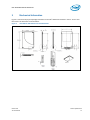
3 Mechanical Information
Figures 1 and 2 show the physical package information for the Intel
®
SSD DC S3610 Series in the 2.5- and 1.8-inch
form factors. All dimensions are in millimeters.
Figure 1: Intel SSD DC S3610 Series 2.5-inch Dimensions
March 2015 Product Specification
331342-003US 15

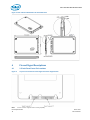
Intel® Solid-State Drive DC S3610 Series
Figure 2. Intel
®
SSD DC S3610 Series 1.8-inch Dimensions
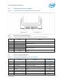
4 Pin and Signal Descriptions
4.1 2.5-inch Form Factor Pin Locations
Figure 3. Layout of 2.5-inch Form Factor Signal and Power Segment Pins
Note: 2.5-inch connector supports built in latching capability.
Product Specification March 2015
16 331342-003US

Intel® Solid-State Drive DC S3610 Series
4.2 1.8-inch Form Factor Pin Locations
Figure 4. Layout of 1.8-inch Form Factor Signal and Power Segment Pins
4.3 Connector Pin Signal Definitions
Table 16: Serial ATA Connector Pin Signal Definitions—2.5-inch and 1.8-inch Form Factors
Pin Function Definition
S1
Ground
1
st
mate
S2
A+
Differential signal pair A
S3
A-
S4
Ground
1
st
mate
S5
B-
Differential signal pair B
S6
B+
S7
Ground
1
st
mate
Note: Key and spacing separate signal and power segments.
4.4 Power Pin Signal Definitions
Table 17: Serial ATA Power Pin Definitions—2.5-inch Form Factors
Pin
1
Function Definition Mating Order
P1
2
Not connected
(3.3V Power)
--
P2
2
Not connected (3.3V Power) --
P3
2
Not connected (3.3V Power; pre-charge) 2
nd
Mate
P4
3,4
Ground Ground 1
st
Mate
P5
3
Ground Ground 1
st
Mate
P6
3
Ground
Ground
1
st
Mate
P7
3,5
V
5
5V Power
1
st
Mate
P8
3,5
V
5
5V Power
2
nd
Mate
March 2015 Product Specification
331342-003US 17

Intel® Solid-State Drive DC S3610 Series
Pin
1
Function Definition Mating Order
P9
3,5
V
5
5V Power
2
nd
Mate
P10
3
Ground
Ground
1
st
Mate
P11
6
DAS
Device Activity Signal
2
nd
Mate
P12
3,4
Ground Ground 1
st
Mate
P13
7
V
12
12V Power 1
st
Mate
P14
7
V
12
12V Power 2
nd
Mate
P15
7
V
12
12V Power
2
nd
Mate
Notes:
1. All pins are in a single row, with a 1.27 mm (0.050-inch) pitch.
2. Pins P1, P2 and P3 are connected together, although they are not connected internally to the device. The host may put 3.3V on these pins.
3. The mating sequence is:
• ground pins P4-P6, P10, P12 and the 5V power pin P7
• signal pins and the rest of the 5V power pins P8-P9
4. Ground connectors P4 and P12 may contact before the other 1st mate pins in both the power and signal connectors to discharge ESD in a suita-
bly configured backplane connector.
5. Power pins P7, P8, and P9 are internally connected to one another within the device.
6. The host may ground P11 if it is not used for Device Activity Signal (DAS).
7. Pins P13, P14 and P15 are internally connected to one another within the device. The host may put 12V on these pins.
Table 18: Serial ATA Power Pin Definitions—1.8-inch Form Factors
Pin Function Definition Mating Order
1
P1
2
V
33
3.3V Power
2
nd
Mate
P2
2
V
33
3.3V Power, per-charge
2
nd
Mate
P3
3
Ground
--
1
st
Mate
P4
3
Ground
--
1
st
Mate
P5
4
V
5
5V Power; not connected.
1
st
Mate
P6
4
V
5
5V Power; not connected.
2
nd
Mate
P7
5
DAS
Device Activity Signal
2
nd
Mate
Key
Key
NC
NC
P8
6
Optional
Manufacturing Test Pin
2
nd
Mate
P9
6
Optional
Manufacturing Test Pin
2
nd
Mate
Notes:
1. All mate sequences assume zero angular offset between connectors.
2. P1 and P2 are internally connected to one another within the device.
3. Ground connectors P3 and P4 may contact before the other 1st mate pins in both the power and signal connectors to discharge ESD in a suitably
configure backplane connector.
4. Pins P5 and P6 are not connected internally to the device but there is an option to connect through a zero ohm stuffing resistor. The
host may put 5V on these pins.
5. The host may ground P7 if it is not used for Device Activity Signal (DAS).
6. P8 and P9 should not be connected by the host.
Product Specification March 2015
18 331342-003US

Intel® Solid-State Drive DC S3610 Series
5 Supported Command Sets
The Intel SSD DC S3610 Series supports all mandatory ATA (Advanced Technology Attachment)
commands defined in the ATA8-ACS specification described in this section.
5.1 ATA General Feature Command Set
The Intel SSD DC S3610 Series supports the ATA General Feature command set (non- PACKET), which
consists of:
• EXECUTE DEVICE DIAGNOSTIC
• SET FEATURES
• IDENTIFY DEVICE
Note: See Appendix A, “IDENTIFY DEVICE Command Data” for details on the sector data returned after
issuing an IDENTIFY DEVICE command.
The Intel SSD DC S3610 Series also supports the following optional commands:
• READ DMA
• WRITE DMA
• READ SECTOR(S)
• READ VERIFY SECTOR(S)
• READ MULTIPLE
• SEEK
• SET FEATURES
• WRITE SECTOR(S)
• SET MULTIPLE MODE
1
• WRITE MULTIPLE
• FLUSH CACHE
• READ BUFFFER
• WRITE BUFFER
• NOP
• DOWNLOAD MICROCODE
• WRITE UNCORRECTABLE EXT
1. The only multiple supported will be multiple 1
5.2 Power Management Command Set
The Intel SSD DC S3610 Series supports the Power Management command set, which consists of:
• CHECK POWER MODE
• IDLE
• IDLE IMMEDIATE
• SLEEP
• STANDBY
• STANDBY IMMEDIATE
5.3 Security Mode Feature Set
The Intel SSD DC S3610 Series supports the Security Mode command set, which consists of:
• SECURITY SET PASSWORD
• SECURITY UNLOCK
• SECURITY ERASE PREPARE
• SECURITY ERASE UNIT
• SECURITY FREEZE LOCK
March 2015 Product Specification
331342-003US 19

Intel® Solid-State Drive DC S3610 Series
• SECURITY DISABLE PASSWORD
5.4 SMART Command Set
The Intel SSD DC S3610 Series supports the SMART command set, which consists of:
• SMART READ DATA
• SMART READ ATTRIBUTE THRESHOLDS
• SMART ENABLE/DISABLE ATTRIBUTE AUTOSAVE
• SMART SAVE ATTRIBUTE VALUES
• SMART EXECUTE OFF-LINE IMMEDIATE
• SMART READ LOG SECTOR
• SMART WRITE LOG SECTOR
• SMART ENABLE OPERATIONS
• SMART DISABLE OPERATIONS
• SMART RETURN STATUS
• SMART ENABLE/DISABLE AUTOMATIC OFFLINE
5.4.1 Attributes
Table 18 lists the SMART attributes supported by the Intel SSD DC S3610 Series and the corresponding status flags
and threshold settings.
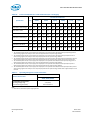
Table 19: SMART Attributes
ID Attribute
Status Flags
Threshold
SP
EC
ER
PE
OC
PW
05h
Re-allocated Sector Count
The raw value of this attribute shows the number of
retired blocks since leaving the factory (grown defect
count).
1 1 0 0 1 0 0 (none)
09h
Power-On Hours Count
The raw value reports power-on time, cumulative over
the life of the SSD, integer number in hour time units.
1 1 0 0 1 0 0 (none)
0Ch
Power Cycle Count
The raw value of this attribute reports the cumulative
number of power cycle events over the life of the device.
1 1 0 0 1 0 0 (none)
AAh
Available Reserved Space (See Attribute E8)
1
1
0
0
1
1
10
ABh
Program Fail Count
The raw value of this attribute shows total count of
program fails and the normalized value, beginning at
100, shows the percent remaining of allowable pro-
gram fails.
1 1 0 0 1 0 0 (none)
ACh
Erase Fail Count
The raw value of this attribute shows total count of
erase fails and the normalized value, beginning at 100,
shows the percent remaining of allowable erase fails.
1 1 0 0 1 0 0 (none)
Product Specification March 2015
20 331342-003US
Page is loading ...
Page is loading ...
Page is loading ...
Page is loading ...
Page is loading ...
Page is loading ...
Page is loading ...
Page is loading ...
Page is loading ...
Page is loading ...
Page is loading ...
Page is loading ...
-
 1
1
-
 2
2
-
 3
3
-
 4
4
-
 5
5
-
 6
6
-
 7
7
-
 8
8
-
 9
9
-
 10
10
-
 11
11
-
 12
12
-
 13
13
-
 14
14
-
 15
15
-
 16
16
-
 17
17
-
 18
18
-
 19
19
-
 20
20
-
 21
21
-
 22
22
-
 23
23
-
 24
24
-
 25
25
-
 26
26
-
 27
27
-
 28
28
-
 29
29
-
 30
30
-
 31
31
-
 32
32


Intel SSDSC2BX012T4 Datasheet
- Category
- Solid state drives
- Type
- Datasheet
- This manual is also suitable for
Ask a question and I''ll find the answer in the document
Finding information in a document is now easier with AI
Related papers
-
Intel SSDMAEMC040G2 Datasheet
-
Intel SSDSC2CW240A310 User manual
-
-
Kingston Technology X25-M SATA II, 80GB, 7.0mm Datasheet
-
Intel SSDMCEAC120B3 Datasheet
-
-
Intel 320 Series User manual
-
-
-
Other documents
-
 Micromat Drive Scope Operating instructions
-
Crucial MTFDDAK100MAN-1S1AA User manual
-
 I/O Magic I120HD25TG Datasheet
-
Avaya 1140E User guide
-
Crucial Micron P300 200GB SATA User manual
-
Integral INSSD120GS25MXP2 User manual
-
-
-
Seagate 600 Pro 240GB SATA 5 Pack User manual
-
Micron MTFDDAA512MAM-1K1 Datasheet

