Page is loading ...

SP605 Hardware
User Guide
UG526 (v1.9) February 14, 2019

SP605 Hardware User Guide www.xilinx.com UG526 (v1.9) February 14, 2019
© Copyright 2009–2019 Xilinx, Inc. Xilinx, the Xilinx logo, Artix, ISE, Kintex, Spartan, Virtex, Zynq, and other designated brands included
herein are trademarks of Xilinx in the United States and other countries. All other trademarks are the property of their respective owners.
DISCLAIMER
The information disclosed to you hereunder (the “Materials”) is provided solely for the selection and use of Xilinx products. To the maximum
extent permitted by applicable law: (1) Materials are made available "AS IS" and with all faults, Xilinx hereby DISCLAIMS ALL
WARRANTIES AND CONDITIONS, EXPRESS, IMPLIED, OR STATUTORY, INCLUDING BUT NOT LIMITED TO WARRANTIES OF
MERCHANTABILITY, NON-INFRINGEMENT, OR FITNESS FOR ANY PARTICULAR PURPOSE; and (2) Xilinx shall not be liable (whether
in contract or tort, including negligence, or under any other theory of liability) for any loss or damage of any kind or nature related to, arising
under, or in connection with, the Materials (including your use of the Materials), including for any direct, indirect, special, incidental, or
consequential loss or damage (including loss of data, profits, goodwill, or any type of loss or damage suffered as a result of any action
brought by a third party) even if such damage or loss was reasonably foreseeable or Xilinx had been advised of the possibility of the same.
Xilinx assumes no obligation to correct any errors contained in the Materials or to notify you of updates to the Materials or to product
specifications. You may not reproduce, modify, distribute, or publicly display the Materials without prior written consent. Certain products are
subject to the terms and conditions of Xilinx’s limited warranty, please refer to Xilinx’s Terms of Sale which can be viewed at
https://www.xilinx.com/legal.htm#tos
; IP cores may be subject to warranty and support terms contained in a license issued to you by Xilinx.
Xilinx products are not designed or intended to be fail-safe or for use in any application requiring fail-safe performance; you assume sole risk
and liability for use of Xilinx products in such critical applications, please refer to Xilinx’s Terms of Sale which can be viewed at
https://www.xilinx.com/legal.htm#tos
.
AUTOMOTIVE APPLICATIONS DISCLAIMER
AUTOMOTIVE PRODUCTS (IDENTIFIED AS “XA” IN THE PART NUMBER) ARE NOT WARRANTED FOR USE IN THE DEPLOYMENT
OF AIRBAGS OR FOR USE IN APPLICATIONS THAT AFFECT CONTROL OF A VEHICLE (“SAFETY APPLICATION”) UNLESS THERE
IS A SAFETY CONCEPT OR REDUNDANCY FEATURE CONSISTENT WITH THE ISO 26262 AUTOMOTIVE SAFETY STANDARD
(“SAFETY DESIGN”). CUSTOMER SHALL, PRIOR TO USING OR DISTRIBUTING ANY SYSTEMS THAT INCORPORATE PRODUCTS,
THOROUGHLY TEST SUCH SYSTEMS FOR SAFETY PURPOSES. USE OF PRODUCTS IN A SAFETY APPLICATION WITHOUT A
SAFETY DESIGN IS FULLY AT THE RISK OF CUSTOMER, SUBJECT ONLY TO APPLICABLE LAWS AND REGULATIONS GOVERNING
LIMITATIONS ON PRODUCT LIABILITY.
Revision History
The following table shows the revision history for this document.
Date Version Revision
10/07/09 1.0 Initial Xilinx release.
11/09/09 1.1 • Updated Figure 1-17 and Figure 1-23.
• Changed speed grade from -2 to -3.
• Miscellaneous typographical edits.
02/01/10 1.1.1 Minor typographical edits to Table 1-24 and Table 1-25.
05/18/10 1.2 Updated Figure 1-2. Added Note 6 to Table 1-11. Updated board connections for
SFP_TX_DISABLE in Table 1-12. Added note about FMC LPC J63 connector in 18. VITA
57.1 FMC LPC Connector. Updated U1 FPGA Pin column for FMC_LA00_CC_P/N in
Table 1-28. Updated description of PMBus Pod and TI Fusion Digital Power Software
GUI in Onboard Power Regulation. Updated Appendix B, VITA 57.1 FMC LPC
Connector Pinout, and Appendix C, Xilinx Design Constraints.
06/16/10 1.3 Updated 2. 128 MB DDR3 Component Memory. Added note 1 to Table 1-30.
09/24/10 1.4 Updated description of Fusion Digital Power Software in Onboard Power Regulation.
02/16/11 1.5 Revised oscillator manufacturer information from Epson to SiTime in Table 1-1. Revised
oscillator manufacturer information from Epson to SiTime on page page 26. Deleted note
on page 44 referring to J55: “Note: This header is not installed on the SP605 as built.”
Revised values for R50 and R216 in Figure 1-12. Revised oscillator manufacturer
information from Epson to SiTime on page page 69.

UG526 (v1.9) February 14, 2019 www.xilinx.com SP605 Hardware User Guide
07/18/11 1.6 Corrected “jitter” to “stability” in section Oscillator (Differential). Revised the feature
and notes descriptions for reference numbers 6 and 12 in Table 1-1. Revised FPGA pin
numbers for ZIO and RZQ in Table 1-4. Added Table 1-29, Table 1-31, and table notes in
Table 1-30.
06/19/12 1.7 Removed reference to FPGA speed grade in 2. 128 MB DDR3 Component Memory.
Added IIC External Access Header. Updated SFP Module connector reference
designator in 8. Multi-Gigabit Transceivers (GTP MGTs).
09/24/12 1.8 Updated Figure 1-2. Added Regulatory and Compliance Information.
02/14/19 1.9 Updated the Electrostatic Discharge Caution section, Appendix C, Xilinx Design
Constraints, and Appendix D, Regulatory and Compliance Information. Updated 2. 128
MB DDR3 Component Memory.
Date Version Revision


SP605 Hardware User Guide www.xilinx.com 5
UG526 (v1.9) February 14, 2019
Revision History . . . . . . . . . . . . . . . . . . . . . . . . . . . . . . . . . . . . . . . . . . . . . . . . . . . . . . . . . . . . . 2
Preface: About This Guide
Guide Contents . . . . . . . . . . . . . . . . . . . . . . . . . . . . . . . . . . . . . . . . . . . . . . . . . . . . . . . . . . . . . . 7
Additional Documentation . . . . . . . . . . . . . . . . . . . . . . . . . . . . . . . . . . . . . . . . . . . . . . . . . . . 7
Additional Support Resources. . . . . . . . . . . . . . . . . . . . . . . . . . . . . . . . . . . . . . . . . . . . . . . . 8
Chapter 1: SP605 Evaluation Board
Overview . . . . . . . . . . . . . . . . . . . . . . . . . . . . . . . . . . . . . . . . . . . . . . . . . . . . . . . . . . . . . . . . . . . . 9
Additional Information . . . . . . . . . . . . . . . . . . . . . . . . . . . . . . . . . . . . . . . . . . . . . . . . . . . . . 9
Features . . . . . . . . . . . . . . . . . . . . . . . . . . . . . . . . . . . . . . . . . . . . . . . . . . . . . . . . . . . . . . . . . 10
Block Diagram . . . . . . . . . . . . . . . . . . . . . . . . . . . . . . . . . . . . . . . . . . . . . . . . . . . . . . . . . . . 11
Related Xilinx Documents. . . . . . . . . . . . . . . . . . . . . . . . . . . . . . . . . . . . . . . . . . . . . . . . . . . 12
Electrostatic Discharge Caution. . . . . . . . . . . . . . . . . . . . . . . . . . . . . . . . . . . . . . . . . . . . . . 12
Detailed Description . . . . . . . . . . . . . . . . . . . . . . . . . . . . . . . . . . . . . . . . . . . . . . . . . . . . . . . . 13
1. Spartan-6 XC6SLX45T-3FGG484 FPGA . . . . . . . . . . . . . . . . . . . . . . . . . . . . . . . . . . . . 15
Configuration . . . . . . . . . . . . . . . . . . . . . . . . . . . . . . . . . . . . . . . . . . . . . . . . . . . . . . . . . 15
I/O Voltage Rails . . . . . . . . . . . . . . . . . . . . . . . . . . . . . . . . . . . . . . . . . . . . . . . . . . . . . . 16
2. 128 MB DDR3 Component Memory . . . . . . . . . . . . . . . . . . . . . . . . . . . . . . . . . . . . . . . 16
3. SPI x4 Flash . . . . . . . . . . . . . . . . . . . . . . . . . . . . . . . . . . . . . . . . . . . . . . . . . . . . . . . . . . . . 19
4. Linear BPI Flash . . . . . . . . . . . . . . . . . . . . . . . . . . . . . . . . . . . . . . . . . . . . . . . . . . . . . . . . 21
FPGA Design Considerations for the Configuration Flash . . . . . . . . . . . . . . . . . . . . . . . 23
5. System ACE CF and CompactFlash Connector. . . . . . . . . . . . . . . . . . . . . . . . . . . . . . 23
6. USB JTAG . . . . . . . . . . . . . . . . . . . . . . . . . . . . . . . . . . . . . . . . . . . . . . . . . . . . . . . . . . . . . 25
7. Clock Generation . . . . . . . . . . . . . . . . . . . . . . . . . . . . . . . . . . . . . . . . . . . . . . . . . . . . . . . 26
Oscillator (Differential) . . . . . . . . . . . . . . . . . . . . . . . . . . . . . . . . . . . . . . . . . . . . . . . . . . 26
Oscillator Socket (Single-Ended, 2.5V or 3.3V) . . . . . . . . . . . . . . . . . . . . . . . . . . . . . . . . 27
SMA Connectors (Differential) . . . . . . . . . . . . . . . . . . . . . . . . . . . . . . . . . . . . . . . . . . . . 28
8. Multi-Gigabit Transceivers (GTP MGTs) . . . . . . . . . . . . . . . . . . . . . . . . . . . . . . . . . . . 28
9. PCI Express Endpoint Connectivity . . . . . . . . . . . . . . . . . . . . . . . . . . . . . . . . . . . . . . . 31
10. SFP Module Connector . . . . . . . . . . . . . . . . . . . . . . . . . . . . . . . . . . . . . . . . . . . . . . . . . 33
11. 10/100/1000 Tri-Speed Ethernet PHY . . . . . . . . . . . . . . . . . . . . . . . . . . . . . . . . . . . . 34
12. USB-to-UART Bridge. . . . . . . . . . . . . . . . . . . . . . . . . . . . . . . . . . . . . . . . . . . . . . . . . . . 36
13. DVI CODEC . . . . . . . . . . . . . . . . . . . . . . . . . . . . . . . . . . . . . . . . . . . . . . . . . . . . . . . . . . 37
14. IIC Bus . . . . . . . . . . . . . . . . . . . . . . . . . . . . . . . . . . . . . . . . . . . . . . . . . . . . . . . . . . . . . . . 38
IIC External Access Header . . . . . . . . . . . . . . . . . . . . . . . . . . . . . . . . . . . . . . . . . . . . . . 39
8-Kb NV Memory . . . . . . . . . . . . . . . . . . . . . . . . . . . . . . . . . . . . . . . . . . . . . . . . . . . . . . 39
15. Status LEDs . . . . . . . . . . . . . . . . . . . . . . . . . . . . . . . . . . . . . . . . . . . . . . . . . . . . . . . . . . . 41
Ethernet PHY Status LEDs . . . . . . . . . . . . . . . . . . . . . . . . . . . . . . . . . . . . . . . . . . . . . . . 42
FPGA INIT and DONE LEDs . . . . . . . . . . . . . . . . . . . . . . . . . . . . . . . . . . . . . . . . . . . . . 43
16. User I/O . . . . . . . . . . . . . . . . . . . . . . . . . . . . . . . . . . . . . . . . . . . . . . . . . . . . . . . . . . . . . 44
User LEDs . . . . . . . . . . . . . . . . . . . . . . . . . . . . . . . . . . . . . . . . . . . . . . . . . . . . . . . . . . . . 44
User Pushbutton Switches . . . . . . . . . . . . . . . . . . . . . . . . . . . . . . . . . . . . . . . . . . . . . . . 45
User DIP Switch . . . . . . . . . . . . . . . . . . . . . . . . . . . . . . . . . . . . . . . . . . . . . . . . . . . . . . . 46
User SIP Header . . . . . . . . . . . . . . . . . . . . . . . . . . . . . . . . . . . . . . . . . . . . . . . . . . . . . . . 47
Table of Contents

6 www.xilinx.com SP605 Hardware User Guide
UG526 (v1.9) February 14, 2019
User SMA GPIO . . . . . . . . . . . . . . . . . . . . . . . . . . . . . . . . . . . . . . . . . . . . . . . . . . . . . . . 48
17. Switches . . . . . . . . . . . . . . . . . . . . . . . . . . . . . . . . . . . . . . . . . . . . . . . . . . . . . . . . . . . . . . 49
Power On/Off Slide Switch SW2 . . . . . . . . . . . . . . . . . . . . . . . . . . . . . . . . . . . . . . . . . . 49
FPGA_PROG_B Pushbutton SW3 (Active-Low). . . . . . . . . . . . . . . . . . . . . . . . . . . . . . . 50
SYSACE_RESET_B Pushbutton SW9 (Active-Low) . . . . . . . . . . . . . . . . . . . . . . . . . . . . 50
System ACE CF CompactFlash Image Select DIP Switch S1 (Active-High) . . . . . . . . . . 51
Mode DIP Switch SW1 (Active-High). . . . . . . . . . . . . . . . . . . . . . . . . . . . . . . . . . . . . . . 52
18. VITA 57.1 FMC LPC Connector . . . . . . . . . . . . . . . . . . . . . . . . . . . . . . . . . . . . . . . . . . 53
19. Power Management . . . . . . . . . . . . . . . . . . . . . . . . . . . . . . . . . . . . . . . . . . . . . . . . . . . . 55
AC Adapter and 12V Input Power Jack/Switch . . . . . . . . . . . . . . . . . . . . . . . . . . . . . . . 55
Onboard Power Regulation . . . . . . . . . . . . . . . . . . . . . . . . . . . . . . . . . . . . . . . . . . . . . . 57
Configuration Options . . . . . . . . . . . . . . . . . . . . . . . . . . . . . . . . . . . . . . . . . . . . . . . . . . . . . . 60
Appendix A: Default Jumper and Switch Settings
Appendix B: VITA 57.1 FMC LPC Connector Pinout
Appendix C: Xilinx Design Constraints
Overview . . . . . . . . . . . . . . . . . . . . . . . . . . . . . . . . . . . . . . . . . . . . . . . . . . . . . . . . . . . . . . . . . . . 65
Appendix D: Regulatory and Compliance Information
CE Directives . . . . . . . . . . . . . . . . . . . . . . . . . . . . . . . . . . . . . . . . . . . . . . . . . . . . . . . . . . . . . . . 67
CE Standards . . . . . . . . . . . . . . . . . . . . . . . . . . . . . . . . . . . . . . . . . . . . . . . . . . . . . . . . . . . . . . . 67
Electromagnetic Compatibility . . . . . . . . . . . . . . . . . . . . . . . . . . . . . . . . . . . . . . . . . . . . . 67
Safety . . . . . . . . . . . . . . . . . . . . . . . . . . . . . . . . . . . . . . . . . . . . . . . . . . . . . . . . . . . . . . . . . . . 67
Markings . . . . . . . . . . . . . . . . . . . . . . . . . . . . . . . . . . . . . . . . . . . . . . . . . . . . . . . . . . . . . . . . . . . 68
Appendix E: References

SP605 Hardware User Guide www.xilinx.com 7
UG526 (v1.9) February 14, 2019
Preface
About This Guide
This manual accompanies the Spartan®-6 FPGA SP605 Evaluation Board and contains
information about the SP605 hardware and software tools.
Guide Contents
This manual contains the following chapters:
• Chapter 1, SP605 Evaluation Board, provides an overview of and details about the
components and features of the SP605 board.
• Appendix A, Default Jumper and Switch Settings.
• Appendix B, VITA 57.1 FMC LPC Connector Pinout.
• Appendix C, Xilinx Design Constraints.
• Appendix D, Regulatory and Compliance Information.
• Appendix E, References.
Additional Documentation
The following documents are available for download at
w
ww.xilinx.com/products/spartan6/.
• Spartan-6 Family Overview
This overview outlines the features and product selection of the Spartan-6 family.
• Spartan-6 FPGA Data Sheet: DC and Switching Characteristics
This data sheet contains the DC and switching characteristic specifications for the
Spartan-6 family.
• Spartan-6 FPGA Packaging and Pinout Specifications
This specification includes the tables for device/package combinations and maximum
I/Os, pin definitions, pinout tables, pinout diagrams, mechanical drawings, and
thermal specifications.
• Spartan-6 FPGA Configuration User Guide
This all-encompassing configuration guide includes chapters on configuration
interfaces (serial and parallel), multi-bitstream management, bitstream encryption,
boundary-scan and JTAG configuration, and reconfiguration techniques.
• Spartan-6 FPGA SelectIO Resources User Guide
This guide describes the SelectIO™ resources available in all Spartan-6 devices.
•Spartan-6 FPGA Clocking Resources User Guide

Preface: About This Guide
8 www.xilinx.com SP605 Hardware User Guide
UG526 (v1.9) February 14, 2019
This guide describes the clocking resources available in all Spartan-6 devices,
including the DCMs and PLLs.
• Spartan-6 FPGA Block RAM Resources User Guide
This guide describes the Spartan-6 device block RAM capabilities.
• Spartan-6 FPGA GTP Transceivers User Guide
This guide describes the GTP transceivers available in the Spartan-6 LXT FPGAs.
• Spartan-6 FPGA DSP48A1 Slice User Guide
This guide describes the architecture of the DSP48A1 slice in Spartan-6 FPGAs and
provides configuration examples.
• Spartan-6 FPGA Memory Controller User Guide
This guide describes the Spartan-6 FPGA memory controller block, a dedicated
embedded multi-port memory controller that greatly simplifies interfacing
Spartan-6 FPGAs to the most popular memory standards.
• Spartan-6 FPGA PCB Designer’s Guide
This guide provides information on PCB design for Spartan-6 devices, with a focus on
strategies for making design decisions at the PCB and interface level.
Additional Support Resources
To search the database of silicon and software questions and answers or to create a
technical support request in the Request Portal, see the Xilinx website
.

SP605 Hardware User Guide www.xilinx.com 9
UG526 (v1.9) February 14, 2019
Chapter 1
SP605 Evaluation Board
Overview
The SP605 board enables hardware and software developers to create or evaluate designs
targeting the Spartan®-6 XC6SLX45T-3FGG484 FPGA.
The SP605 provides board features common to many embedded processing systems. Some
commonly used features include: a DDR3 component memory, a 1-lane PCI Express®
interface, a tri-mode Ethernet PHY, general purpose I/O, and a UART. Additional user
desired features can be added through mezzanine cards attached to the onboard high
speed VITA-57 FPGA Mezzanine Connector (FMC) low pin count (LPC) connector.
Features provides a general listing of the board features with details provided in Detailed
Description.
Additional Information
Additional information and support material is located at:
• Spartan-6 FPGA SP605 Evaluation Kit
This information includes:
• Current version of this user guide in PDF format
• Example design files for demonstration of Spartan-6 FPGA features and technology
• Demonstration hardware and software configuration files for the System ACE™ CF
controller, Platform Flash configuration storage device, and linear flash chip
• Reference Design Files
• Schematics in PDF format and DxDesigner schematic format
• Bill of materials (BOM)
• Printed-circuit board (PCB) layout in Allegro PCB format
• Gerber files for the PCB (Many free or shareware Gerber file viewers are available on
the Internet for viewing and printing these files.)
• Additional documentation, errata, frequently asked questions, and the latest news
For information about the Spartan-6 family of FPGA devices, including product highlights,
data sheets, user guides, and application notes, see the S
partan-6 FPGA website.

10 www.xilinx.com SP605 Hardware User Guide
UG526 (v1.9) February 14, 2019
Chapter 1: SP605 Evaluation Board
Features
The SP605 board provides the following features (see Figure 1-2 and Table 1-1):
• 1. Spartan-6 XC6SLX45T-3FGG484 FPGA
• 2. 128 MB DDR3 Component Memory
• 3. SPI x4 Flash
• 4. Linear BPI Flash
• 5. System ACE CF and CompactFlash Connector
• 6. USB JTAG
• 7. Clock Generation
• Fixed 200 MHz oscillator (differential)
• Socket with a 2.5V 27MHz oscillator (single-ended)
• SMA connectors (differential)
• SMA connectors for MGT clocking (differential)
• 8. Multi-Gigabit Transceivers (GTP MGTs)
• FMC LPC connector
•SMA
•PCIe
• SFP module connector
• 9. PCI Express Endpoint Connectivity
•Gen1 x1
• 10. SFP Module Connector
• 11. 10/100/1000 Tri-Speed Ethernet PHY
• 12. USB-to-UART Bridge
• 13. DVI CODEC
• 14. IIC Bus
• IIC EEPROM - 1KB
•DVI CODEC
• DVI connector
• FMC LPC connector
• SFP Module connector
• 15. Status LEDs
•Ethernet Status
•FPGA INIT
•FPGA DONE
• 16. User I/O
•USER LED GPIO
• User pushbuttons
•CPU Reset pushbutton
•User DIP switch - GPIO
• User SMA GPIO connectors

SP605 Hardware User Guide www.xilinx.com 11
UG526 (v1.9) February 14, 2019
Overview
• 17. Switches
• Power On/Off slide switch
• System ACE CF Reset pushbutton
• System ACE CF bitstream image select DIP switch
•Mode DIP switch
• 18. VITA 57.1 FMC LPC Connector
• 19. Power Management
• AC Adapter and 12V Input Power Jack/Switch
• Onboard Power Regulation
• Configuration Options
• 3. SPI x4 Flash (both onboard and off-board)
• 4. Linear BPI Flash
• 5. System ACE CF and CompactFlash Connector
• 6. USB JTAG
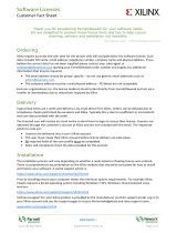
Block Diagram
The following figure shows a high-level block diagram of the SP605 and its peripherals.
X-Ref Target - Figure 1-1
Figure 1-1: SP605 Features and Banking
Spartan-6
XC6SLX45T-3FGG484
U1
PCIe 125 MHz Clk
SMA REFCLK
SFPCLK
FMC GBTCLK
Bank 0
2.5V
Bank 1
2.5V
Bank 3
1.5V
= Level Shifter
DVI IIC Bus
Bank 2
2.5V
Part of
FMC-LPC
Expansion
Connector
LED
DIP Switch
User SMA x2
1-Lane I/Fs:
PCIe Edge Conn.
SMA x4 SFP
FMC-LPC
10/100/1000
Ethernet PHY,
Status LEDs,
and Connector
SFP IIC Bus
JTAG
System ACE
JTAG
JTAG
MPU I/F
USB JTAG Logic
and USB Mini-B
Connector
DDR3
Component
Memory
Pushbuttons
DIP Switch
LED,
DIP Switch
SPI x4,
SPI Header
Part of FMC-LPC
Expansion Conn.
GPIO Header
USB UART and
USB Mini-B
Connector
DVI Codec and
DVI Connector
Parallel Flash
Main IIC Bus
UG526_01_110409
DED
MGTs
L/S
L/S
L/S

12 www.xilinx.com SP605 Hardware User Guide
UG526 (v1.9) February 14, 2019
Chapter 1: SP605 Evaluation Board
Related Xilinx Documents
Prior to using the SP605 Evaluation Board, users should be familiar with Xilinx resources.
See the following locations for additional documentation on Xilinx tools and solutions:
• I
SE
• Answer Browser
• Design Hub
Electrostatic Discharge Caution
Caution! ESD can damage electronic components when they are improperly
handled, and can result in total or intermittent failures. Always follow ESD-
prevention procedures when removing and replacing components.
To prevent ESD damage:
• Use an ESD wrist or ankle strap and ensure that it makes skin contact. Connect the
equipment end of the strap to an unpainted metal surface on the chassis.
• Avoid touching the adapter against your clothing. The wrist strap protects
components from ESD on the body only.
• Handle the adapter by its bracket or edges only. Avoid touching the printed circuit
board or the connectors.
• Put the adapter down only on an anti-static surface such as the bag supplied in your
kit.
• If you are returning the adapter to Xilinx Product Support, place it back in its anti-
static bag immediately.

SP605 Hardware User Guide www.xilinx.com 13
UG526 (v1.9) February 14, 2019
Detailed Description
Detailed Description
Figure 1-2 shows a board photo with numbered features corresponding to Table 1-1 and
the section headings in this document.
The numbered features in Figure 1-2 correlate to the features and notes listed in Table 1-1.
X-Ref Target - Figure 1-2
Figure 1-2: SP605 Board
15e
13
16b
19
7a
15h
1
2
3
4
8
15g
5
17c
9
3, 14 (on back side)
7b
10
18
6
12
16c
11
17b
15b 15a
17a
19b
15d
UG526_02 _092412
15c
8
7c
16d
17d
16a
15f
Table 1-1: SP605 Features
Number Feature Notes
Schematic
Page
1 Spartan-6 FPGA XC6SLX45T-3FGG484 FPGA 2–7
2 DDR3 Component Memory Micron MT41J64M16LA-187E 9
3
SPI Header Ext. x4
SPI Flash x4 (on backside)
Winbond W25Q64FVSFIG 18
4 Linear BPI Flash x16 Numonyx JS28F256P30T95 19
5
System ACE CompactFlash
Socket
XCCACE-TQ144I Controller 20
6
USB UART (USB-to-UART
Bridge)
Silicon Labs CP2103GM 32

14 www.xilinx.com SP605 Hardware User Guide
UG526 (v1.9) February 14, 2019
Chapter 1: SP605 Evaluation Board
7
Clock Generation
200 MHz OSC, oscillator socket,
SMA connectors
13, 14
a. 200 MHz oscillator SiTime 200 MHz 2.5V LVDS 14
b. Oscillator socket, single-
ended, LVCMOS
MMD Components 2.5V 27 MHz 14
c. SMA connectors SMA pair P(J41) / N(J38) 13
8
GTP port SMA x4 and
MGT Clocking SMA (REFCLK)
MGT RX,TX Pairs x4 SMA MGT
REFCLK x2 SMA
13
9 PCIe 1-lane edge conn.(Gen 1) Card Edge Connector, 1-lane 12
10 SFP Module Cage/Connector AMP 136073-1 12
11 Ethernet 10/100/1000 Marvell M88E1111 EPHY 11
12 USB JTAG Conn. (USB Mini-B) USB JTAG Download Circuit 15
13 DVI Codec and Video Connector Chrontel CH7301C-TF 16,17
14 IIC EEPROM (on backside) ST Micro M24C08-WDW6TP 15
15
Status LEDs
10, 11, 14,
18, 20, 25,
27, 31, 33
a. FMC Power Good 10
b. System ACE CF Status 11
c. FPGA INIT and DONE 14
d. Ethernet PHY Status 18
e. JTAG USB Status 20
f. FPGA Awake 27
g. TI Power Good 31
h. MGT AVCC, DDR3 Term
Pwr Good
33
16
a. User LEDs (4) Red LEDs (active-High) 14
b. User Pushbuttons (4) Active-High 14
c. User DIP Switch (4-pole) 4-pole (active-High) 14
d. User SMA (2) GPIO x2 SMA 13
Table 1-1: SP605 Features (Cont’d)
Number Feature Notes
Schematic
Page

SP605 Hardware User Guide www.xilinx.com 15
UG526 (v1.9) February 14, 2019
Detailed Description
1. Spartan-6 XC6SLX45T-3FGG484 FPGA
A Xilinx Spartan-6 XC6SLX45T-3FGG484 FPGA is installed on the SP605 Evaluation Board.
See the Spartan-6 FPGA Data Sheet (DS162). [Ref 1]
Configuration
The SP605 supports configuration in the following modes:
• JTAG (using the included USB-A to Mini-B cable)
•JTAG (using System ACE CF and CompactFlash card)
•Master SPI x4
• Master SPI x4 with off-board device
• Linear BPI Flash
For details on configuring the FPGA, see Configuration Options.
Mode switch SW1 (see Table 1-32) is set to 10 = Slave SelectMAP to choose the System
ACE CF default configuration.
See the Spartan-6 FPGA Configuration User Guide (UG380) for more information. [Ref 2]
17
Switches
Power, Configuration,
Pushbutton Switches
14, 18, 20,
25
a. SP605 Power On-Off Slide
Switch
25
b. FPGA Mode DIP Switch 18
c. System ACE CF
Configuration DIP Switch
20
d. FPGA PROG, CPU Reset,
and System ACE CF Reset
Pushbutton Switches
14, 20
18 FMC LPC Connector Samtec ASP-134603-01 10
19
a. Power Management
Controller
2x TI UCD9240PFC 21, 26
b. Mini-Fit Type 6-Pin, ATX
Type 4-pin
12V input power connectors 25
Table 1-1: SP605 Features (Cont’d)
Number Feature Notes
Schematic
Page

16 www.xilinx.com SP605 Hardware User Guide
UG526 (v1.9) February 14, 2019
Chapter 1: SP605 Evaluation Board
I/O Voltage Rails
There are four available banks on the XC6SLX45T-3FGG484 device. Banks 0, 1, and 2 are
connected for 2.5V I/O. Bank 3 is used for the 1.5V DDR3 component memory interface of
Spartan-6 FPGA’s hard memory controller. The voltage applied to the FPGA I/O banks
used by the SP605 board is summarized in Table 1-2.
See the X
ilinx Spartan-6 FPGA documentation for more information.
2. 128 MB DDR3 Component Memory
The SP605 128 MB 16-bit wide DDR3 memory consists of a single 1 Gb x 16 SDRAM U42
wired to Bank 3 (V
cco
= 1.5V) of the U1 XC6SLX45T FPGA. The Spartan-6 FPGA hard
memory controller is used for data transfer across the DDR3 memory interface’s 16-bit
data path using SSTL15 signaling.
•Manufacturer: Micron
• Part Number: MT41J64M16LA-187E
•Description:
• 1 Gb: 128 MB (64 Mb x 16)
• 1.5V 96-ball FBGA
• Performance: up to DDR3-1066
The SP605 board supports the “standard” VCCINT setting of 1.20V ± 5%. This setting
provides memory controller block (MCB) performance of 667 MT/s for DDR3 memory.
The SP605 XC6SLX45T FPGA DDR interface performance is documented in the Spartan-6
FPGA Data Sheet: DC and Switching Characteristics (DS162). [Ref 1]
Signal integrity is maintained through DDR3 resistor terminations and memory on-die
terminations (ODT), as shown in Table 1-3 and Table 1-4.
Table 1-2: I/O Voltage Rail of FPGA Banks
FPGA Bank I/O Voltage Rail
02.5V
12.5V
22.5V
31.5V
Table 1-3: Termination Resistor Requirements
Signal Name Board Termination On-Die Termination
MEM1_A[14:0] 49.9Ω to V
TT
–
MEM1_BA[2:0] 49.9Ω to V
TT
–
MEM1_RAS_N 49.9Ω to V
TT
–
MEM1_CAS_N 49.9Ω to V
TT
–
MEM1_WE_N 49.9Ω to V
TT
–
MEM1_CS_N 100Ω to GND –
MEM1_CKE 4.7 KΩ to GND –

SP605 Hardware User Guide www.xilinx.com 17
UG526 (v1.9) February 14, 2019
Detailed Description
Table 1-5 shows the connections and pin numbers for the DDR3 Component Memory.
MEM1_ODT 4.7 KΩ to GND –
MEM1_DQ[15:0] – ODT
MEM1_UDQS[P,N], MEM1_LDQS[P,N] – ODT
MEM1_UDM, MEM1_LDM – ODT
MEM1_CK[P,N]
100Ω differential at memory
component
–
Notes:
1. Nominal value of V
TT
for DDR3 interface is 0.75V.
Table 1-4: FPGA On-Chip (OCT) Termination External Resistor Requirements
U1 FPGA Pin FPGA Pin Number Board Connection for OCT
ZIO M7 No Connect
RZQ K7 100Ω to GROUND
Table 1-5: DDR3 Component Memory Connections
U1 FPGA
Pin
Schematic Net Name
Memory U42
Pin Number Pin Name
K2 MEM1_A0 N3 A0
K1 MEM1_A1 P7 A1
K5 MEM1_A2 P3 A2
M6 MEM1_A3 N2 A3
H3 MEM1_A4 P8 A4
M3 MEM1_A5 P2 A5
L4 MEM1_A6 R8 A6
K6 MEM1_A7 R2 A7
G3 MEM1_A8 T8 A8
G1 MEM1_A9 R3 A9
J4 MEM1_A10 L7 A10/AP
E1 MEM1_A11 R7 A11
F1 MEM1_A12 N7 A12/BCN
J6 MEM1_A13 T3 NC/A13
H5 MEM1_A14 T7 NC/A14
J3 MEM1_BA0 M2 BA0
J1 MEM1_BA1 N8 BA1
H1 MEM1_BA2 M3 BA2
Table 1-3: Termination Resistor Requirements (Cont’d)
Signal Name Board Termination On-Die Termination

18 www.xilinx.com SP605 Hardware User Guide
UG526 (v1.9) February 14, 2019
Chapter 1: SP605 Evaluation Board
R3 MEM1_DQ0 G2 DQ6
R1 MEM1_DQ1 H3 DQ4
P2 MEM1_DQ2 E3 DQ0
P1 MEM1_DQ3 F2 DQ2
L3 MEM1_DQ4 H7 DQ7
L1 MEM1_DQ5 H8 DQ5
M2 MEM1_DQ6 F7 DQ1
M1 MEM1_DQ7 F8 DQ3
T2 MEM1_DQ8 C2 DQ11
T1 MEM1_DQ9 C3 DQ9
U3 MEM1_DQ10 A2 DQ13
U1 MEM1_DQ11 D7 DQ8
W3 MEM1_DQ12 A3 DQ15
W1 MEM1_DQ13 C8 DQ10
Y2 MEM1_DQ14 B8 DQ14
Y1 MEM1_DQ15 A7 DQ12
H2 MEM1_WE_B L3 WE_B
M5 MEM1_RAS_B J3 RAS_B
M4 MEM1_CAS_B K3 CAS_B
L6 MEM1_ODT K1 ODT
K4 MEM1_CLK_P J7 CLK_P
K3 MEM1_CLK_N K7 CLK_N
F2 MEM1_CKE K9 CKE
N3 MEM1_LDQS_P F3 LDQS_P
N1 MEM1_LDQS_N G3 LDQS_N
V2 MEM1_UDQS_P C7 UDQS_P
V1 MEM1_UDQS_N B7 UDQS_N
N4 MEM1_LDM E7 LDM
P3 MEM1_UDM D3 UDM
E3 MEM1_RESET_B T2 RESET_B
Table 1-5: DDR3 Component Memory Connections (Cont’d)
U1 FPGA
Pin
Schematic Net Name
Memory U42
Pin Number Pin Name

SP605 Hardware User Guide www.xilinx.com 19
UG526 (v1.9) February 14, 2019
Detailed Description
See the Micron Technology, Inc. DDR3 SDRAM Specification for more information. [Ref 15]
Also, see the Spartan-6 FPGA Memory Controller User Guide (UG388). [Ref 3]
3. SPI x4 Flash
The Xilinx Spartan-6 FPGA hosts a SPI interface which is visible to the Xilinx iMPACT
configuration tool. The SPI memory device operates at 3.0V; the Spartan-6 FPGA I/Os are
3.3V tolerant and provide electrically compatible logic levels to directly access the SPI flash
through a 2.5V bank. The XC6SLX45T-3FGG484 is a master device when accessing an
external SPI flash memory device.
The SP605 SPI interface has two parallel connected configuration options (Figure 1-3): an
SPI X4 (Winbond W25Q64FVSFIG) 64-Mb flash memory device (U32) and a flash
programming header (J17). J17 supports a user-defined SPI mezzanine board. The SPI
configuration source is selected via SPI select jumper J46. For details on configuring the
FPGA, see Configuration Options.
X-Ref Target - Figure 1-3
Figure 1-3: J17 SPI Flash Programming Header
SPI Prog
FPGA_D1_MISO2
J17
1
2
3
4
5
6
7
8
9
FPGA_D2_MISO3
FPGA_PROG_B
FPGA_MOSI_CSI_B_MISO0
SPI_CS_B
FPGA_CCLK
FPGA_D0_DIN_MISO_MISO1
UG526_03_092409
GND
VCC3V3
Silkscreen
TMS
TDI
TDO
TCK
GND
3V3
HDR_1X9

20 www.xilinx.com SP605 Hardware User Guide
UG526 (v1.9) February 14, 2019
Chapter 1: SP605 Evaluation Board
See the Winbond Serial Flash Memory Data Sheet for more information. [Ref 16]
See the XPS Serial Peripheral Interface Data Sheet (DS570) for more information. [Ref 4]
X-Ref Target - Figure 1-4
Figure 1-4: SPI Flash Interface Topology
Table 1-6: SPI x4 Memory Connections
U1 FPGA
Pin
Schematic Net Name
SPI MEM U32 SPI HDR J17
Pin # Pin Name Pin # Pin Name
AB2 FPGA_PROG_B – – 1 –
T14 FPGA_D2_MISO3 1 IO3_HOLD_B 2 –
R13 FPGA_D1_MISO2_R 9 IO2_WP_B 3 –
AA3 SPI_CS_B – – 4 TMS
AB20 FPGA_MOSI_CSI_B_MISO0 15 DIN 5 TDI
AA20 FPGA_D0_DIN_MISO_MISO1 8 IO1_DOUT 6 TDO
Y20 FPGA_CCLK 16 CLK 7 TCK
– – – –8GND
– – – – 9 VCC3V3
J46.2
(1)
SPIX4_CS_B 7 CS_B – –
Notes:
1. Not a U1 FPGA pin
U1
FPGA SPI Interface
U32
J17
SPI x4
Flash
Memory
Winbond
W25Q64FVSFIG
SPI Program
Header
SPI Select
Jumper
ON = SPI X4 U32
OFF = SPI EXT. J17
SPIX4_CS_B
DIN, DOUT, CCLK
SPI_CS_B
2
J46
1
UG526_04_020819
/