Nvidia GeForce GTX 200 GPU Technical Brief
- Category
- Graphics cards
- Type
- Technical Brief
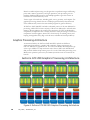
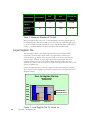
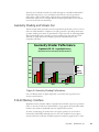
Nvidia GeForce GTX 200 GPU is a second-generation unified graphics and computing architecture. It has double the performance of the previous generation and incorporates both a second-generation unified graphics architecture and an enhanced high-performance, parallel-computing architecture. With this upgrade, you can expect convincing facial and character animation, multiple ultra-high polygon characters in complex environments, advanced volumetric effects (smoke, fog, mist, etc.
Nvidia GeForce GTX 200 GPU is a second-generation unified graphics and computing architecture. It has double the performance of the previous generation and incorporates both a second-generation unified graphics architecture and an enhanced high-performance, parallel-computing architecture. With this upgrade, you can expect convincing facial and character animation, multiple ultra-high polygon characters in complex environments, advanced volumetric effects (smoke, fog, mist, etc.


-
 1
1
-
 2
2
-
 3
3
-
 4
4
-
 5
5
-
 6
6
-
 7
7
-
 8
8
-
 9
9
-
 10
10
-
 11
11
-
 12
12
-
 13
13
-
 14
14
-
 15
15
-
 16
16
-
 17
17
-
 18
18
-
 19
19
-
 20
20
-
 21
21
-
 22
22
-
 23
23


Nvidia GeForce GTX 200 GPU Technical Brief
- Category
- Graphics cards
- Type
- Technical Brief
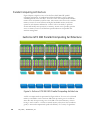
Nvidia GeForce GTX 200 GPU is a second-generation unified graphics and computing architecture. It has double the performance of the previous generation and incorporates both a second-generation unified graphics architecture and an enhanced high-performance, parallel-computing architecture. With this upgrade, you can expect convincing facial and character animation, multiple ultra-high polygon characters in complex environments, advanced volumetric effects (smoke, fog, mist, etc.
Ask a question and I''ll find the answer in the document
Finding information in a document is now easier with AI
Related papers
-
Nvidia GeForce GT 630 Quick Manual
-
-
-
-
-
-
-
-
-
Nvidia GeForce GTX 460 Installation guide