
PCI-7432 / 7433 / 7434
cPCI-7432 / 7433 / 7434
64 Channels Isolated
Digital I/O / Digital Input /
Digital Output Card


@Copyright 1998~1999 ADLink Technology Co., Ltd.
All Rights Reserved.
Manual Rev. 2.10: November 28, 1998
The information in this document is subject to change without prior notice in
order to improve reliability, design and function and does not represent a
commitment on the part of the manufacturer.
In no event will the manufacturer be liable for direct, indirect, special,
incidental, or consequential damages arising out of the use or inability to use
the product or documentation, even if advised of the possibility of such
damages.
This document contains proprietary information protected by copyright. All
rights are reserved. No part of this manual may be reproduced by any
mechanical, electronic, or other means in any form without prior written
permission of the manufacturer.
Trademarks
NuDAQ
, NuIPC
, PCI-7432, PCI-7433, PCI-7434, cPCI-7432, cPCI-7433,
cPCI-7434 are registered trademarks of ADLink Technology Co., Ltd. Other
product names mentioned herein are used for identification purposes only
and may be trademarks and/or registered trademarks of their respective
companies.

Contents •• i
CONTENTS
INTRODUCTIONINTRODUCTION .................................................................................................... 11
1.1 Features ................................................................... 2
1.2 Applications ................................................................... 3
1.3 Specifications ................................................................... 3
INSTALLATIONINSTALLATION.................................................................................................................. 55
2.1 What You Have ................................................................... 5
2.2 Unpacking ................................................................... 6
2.3 Device Installation for Windows 95 ....................................... 7
2.4 PCI-7432/33/34's Layout ...................................................... 8
2.5 PCI-7432/33/34 Installation Outline ...................................... 9
2.5.1 Hardware configuration........................................................9
2.5.2 PCI slot selection .................................................................9
2.5.3 Installation Procedures.........................................................9
2.5.4 Running the 7432UTIL.EXE .................................................9
2.6 Connector Pin Assignment of PCI-7432................................ 10
2.7 Connector Pin Assignment of PCI-7433................................ 11
2.8 Connector Pin Assignment of PCI-7434................................ 12
REGISTER FORMAT & CONNECTIONREGISTER FORMAT & CONNECTION...................................................... 1313
3.1 I/O Registers Format............................................................ 13
3.2 Digital Input Register............................................................ 14
3.3 Digital Output Register ......................................................... 15
3.4 Isolated Digital Input Channels ............................................. 16
3.5 Isolated Digital Output Channels........................................... 17
C/C++ LIBRARIESC/C++ LIBRARIES .................................................................................................... 1919
4.1 Installation ................................................................... 19
4.1.1 Installation ..........................................................................19
4.2 Running Testing Utility (7432UTIL.EXE)................................ 22
4.3 I_EEPROM ................................................................... 22
4.3.1 Running I_eeprom.exe..........................................................22
4.4 Software Driver Naming Convention..................................... 23
4.5 _7432_Initial / _7433_Initial / _7434_Initial ........................... 23
4.6 _7432_DI / _7433_DI_HiDW / _7433_DI_LoDW................... 24
4.7 _7432_DO / _7434_DO_HiDW / _7434_DO_LoDW.............. 25
4.8 _7432_Set_INT_Control / _7433_Set_INT_Control............... 27
4.9 _7432_Get_INT_Status / _7433_Get_INT_Status................. 28
4.10 _7432_INT_Enable / _7433_INT_Enable.............................. 29
4.11 _7432_INT_Disable / _7433_INT_Disable............................ 30

ii •• Contents
PRODUCT WARRANTY/SERVICE .................................................................. 3131

Introduction •• 1
1
Introduction
The PCI-7432 provides 64 isolated digital I/O (32 Isolated inputs
and 32 isolated outputs), PCI-7433 provides 64 isolated digital
input and PCI-7434 provides 64 isolated digital output. The
isolated I/O channels are isolated to 5000 Vdc (excluding cables),
both channel-to-channel and channel-to-computer. It protects
your computer against damage caused by accidental contact with
high external voltage and elimates troublesome ground loops.
The PCI-7432, 7433, and 7434 uses ASIC PCI controller to
interface the board to the PCI bus. The ASIC fully implement the
PCI local bus specification Rev 2.0. All bus relative
configurations, such as base memory and interrupt assignment,
are automatically controlled by BIOS software. It does not need
any user interaction and pre-study for the configurations. This
removes the burden of searching for a conflict-free configuration,
which can be very time consuming and difficult with some other
bus standards.
Software Supporting :
There are several software options help you get your application
running quickly and easily.
1. Linking with data acquisition software packages :
. DasyLab 4.0
. LabVIEW 5.0
. InTouch 7.0
2. Custom Program :

2 •• Introduction
For the customers who are writing their own programs, the
PCI-7432/33/34 are supported by a comprehensive set of
drivers and programming tools. These software supports are
available in multiple platform.
.C/C++ program library for MS-DOS and DLL library for
Window 95, shipped with board.
.PCIS-DASK/NT:Advanced data acquisition software kit and
DLL driver for Win-NT
.DAQBench: ActiveX (OLE) controls for Win-NT
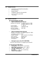
1.1 Features
The PCI-743X Isolated D/I cards provide the following advanced
features:
PCI-7432 PCI-7433 PCI-7434
cPCI-7432 cPCI-7433 CPCI-7434
32 Isolated Digital Input / Output Channels
√
-- --
64 Isolated Digital Input Channels --
√
--
64 Isolated Digital Output Channels -- --
√
High output driving capability
√
--
√
500mA sink current on isolated output
channels
√ -- √
5000 Vrms high voltage isolation
√ √ √
External interrupt signal
√ √
--
Dual interrupt trigger
√ √
--
Up to 24V voltage protection for isolated
input
√ √ --
100-pin SCSI-II connector
√ √ √

Introduction •• 3
1.2 Applications
• Laboratory and Industrial automation
• Watchdog timer
• Event counter
• Frequency counter and generator
• Low level pulse generator
• Time delay
1.3 Specifications
♦♦ Isolated Digital I/O (DIO)
• Optical Isolated Input Channel
Number of Channels: 32 digital inputs for 7432
64 digital inputs for 7433
Input Voltage: 5 - 24V dc
Input resistance: 1.2KΩ @ 0.5W
Isolated voltage: 5000 Vdc
Throughput:10K Hz
• Optical isolated Output channel
Number of Channels: 32 digital outputs for 7432
64 digital outputs for 7434
Output Voltage: open collector 5 to 35Vdc
Sink Current: 500mA max.
Isolated voltage: 5000 Vdc
Throughput: 10K Hz
• Interrupt sources (for PCI-7432/7433)
Channel 0 and channel 1 of digital input channels
♦ General Specifications
• Connector : 100-pin SCSI-II connector
• Operating Temperature : 0° C ~ 60° C
• Storage Temperature : -20° C ~ 80° C
• Humidity : 5 ~ 95%, non-condensing
• Power Consumption :

4 •• Introduction
8PCI-7432: +5V @ 530 mA typical
8PCI-7433: +5V @ 500 mA typical
8PCI-7434: +5V @ 560 mA typical
8cPCI-7432: +5V @ 455 mA typical
8cPCI-7433: +5V @ 500 mA typical
8cPCI-7434: +5V @ 430 mA typical
• Dimension :
8PCI-7432/33/34: Compact size only 98mm(H) X 173mm(L)
8cPCI-7432/33/34: Standard 3U CompactPCI form factor

Installation •• 5
2
InstallationInstallation
This chapter describes the configurations of the PCI-7432/33/34
and teaches users to install the PCI-7432/33/34. At first, the
contents in the package and unpacking information that you
should care about are described. The PCI-7432/33/34 are plug-
and-play; it is very easy to install into any PC system with PCI
slots.
2.1 What You Have
In addition to this User's Manual, the package includes the
following items:
• PCI-7432, PCI-7433, or PCI-7434 Isolated Digital I/O Card
• Manual & Software Utility CD
If any of these items is missing or damaged, contact the dealer
from whom you purchased the product. Save the shipping
materials and carton in case you want to ship or store the product
in the future.

6 •• Installation
2.2 Unpacking
Your PCI-7432/33/34 card contains sensitive electronic
components that can be easily damaged by static electricity.
The card should be done on a grounded anti-static mat. The
operator should be wearing an anti-static wristband, grounded at
the same point as the anti-static mat.
Inspect the card module carton for obvious damage. Shipping
and handling may cause damage to your module. Be sure there
are no shipping and handing damages on the module before
processing.
After opening the card module carton, extract the system module
and place it only on a grounded anti-static surface component
side up.
Again inspect the module for damage. Press down on all the
socketed IC's to make sure that they are properly seated. Do this
only with the module place on a firm flat surface.
Note :DO NOT APPLY POWER TO THE CARD IF IT HAS BEEN
DAMAGED.
Now you are ready to install your PCI-7432/33/34 card.

Installation •• 7
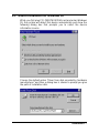
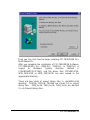
2.3 Device Installation for Windows 95
While you first plug PCI-7432/7433/7434 card and enter Windows
95, the system will detect this device automatically and show the
following dialog box that prompts you to select the device
information source.
Choose the default option “Driver from disk provided by hardware
manufacturer” and then a dialog box is shown to prompt you give
the path of installation disk.

8 •• Installation
Place ADLink’s “Manual & Software Utility” CD into the
appropriate CD driver. Type “X:\Software\Pci_Card\7432\Win95”,
“X:\Software\Pci_Card\7433\Win95” or
“X:\Software\Pci_Card\7434\Win95” (these directories include
PCI-7432/33/34 device information files “7432.inf”, “7433.inf”, or
“7434.inf”) in the input field (X indicates the CD ROM driver)
and then click OK. The system will start the installation of PCI-
7432/33/34 device.
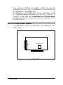
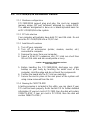
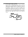
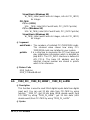
2.4 PCI-7432/33/34's Layout
PCI-7432/33/34’s layout are quite alike. The following is PCI-
7432’s layout.
CN1
PCI Connector Chip
Figure 2.1

Installation •• 9
2.5 PCI-7432/33/34 Installation Outline
2.5.1 Hardware configuration
PCI-7432/33/34 support plug and play, the card can requests
memory usage (I/O port locations) assigned by system BIOS.
The address assignment is done on a board-by-board basis for
all PCI-7432/33/34 in the system.
2.5.2 PCI slot selection
Your computer will probably have both PCI and ISA slots. Do not
force the PCI-7432/33/34 into a PC/AT slot.
2.5.3 Installation Procedures
1. Turn off your computer
2. Turn off all accessories (printer, modem, monitor, etc.)
connected to computer.
3. Remove the cover from your computer.
4. Select a 32-bit PCI expansion slot. PCI slots are short than
ISA or EISA slots and are usually white or ivory.
Caution !! Don‘t put PCI-7432/33/34 card into
ISA or EISA slot.
5. Before handling the PCI-7432/33/34, discharge any static
buildup on your body by touching the metal case of the
computer. Hold the edge and do not touch the components.
6. Position the board into the PCI slot you selected.
7. Secure the card in place at the rear panel of the system unit
using screw removed from the slot.
2.5.4 Running the 7432UTIL.EXE
A testing program is included in this utility, you can check if your
PCI card can work properly. Refer Section 5.2 for further detailed
information.(If your pci card is PCI-7433, then the disk will contain
7433UTIL.EXE. If your pci card is PCI-7434, then the disk will
contain 7434UTIL.EXE.)

10 •• Installation
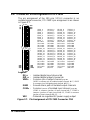
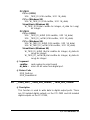
2.6 Connector Pin Assignment of PCI-7432
The pin assignment of the 100 pins SCSI-II connector is an
isolated signal connector, PCI-7432’s pin assignment is as shown
in Figure 2.7.
(1)
(2)
(3)
(52)
(53)
(51)
(48)
(49)
(50)
(98)
(99)
(100)
Legend:
IDI_n : Isolated digital input channel #n
IDO_n : Isolated digital output channel #n
VDDm : Common pin of output channel group #m
(VDD1 is common pin of isolated output channel #0~7, VDD2
is common pin of isolated output channel #8~15,…)
IGND : Ground return path of isolated output channels
COMm : Common junction of isolated input channel group #m
(COM1 is common junction of input channel #0~7, COM2 is
common junction of input channel #8~15, COM3 is common
junction of input channel #16~15, … )
V5V : Onboard un-regulated 5V power supply output
Figure 2.7. Pin Assignment of PCI-7432 Connector CN1
(1) IDI_0 (26) IDO_0 (51) IDI_8 (76) IDO_8
(2) IDI_1 (27) IDO_1 (52) IDI_9 (77) IDO_9
(3) IDI_2 (28) IDO_2 (53) IDI_10 (78) IDO_10
(4) IDI_3 (29) IDO_3 (54) IDI_11 (79) IDO_11
(5) IDI_4 (30) IDO_4 (55) IDI_12 (80) IDO_12
(6) IDI_5 (31) IDO_5 (56) IDI_13 (81) IDO_13
(7) IDI_6 (32) IDO_6 (57) IDI_14 (82) IDO_14
(8) IDI_7 (33) IDO_7 (58) IDI_15 (83) IDO_15
(9) COM1 (34) VDD1 (59) COM2 (84) VDD2
(10) COM1 (35) IGND (60) COM2 (85) IGND
(11) COM1 (36) IGND (61) COM2 (86) IGND
(12) COM1 (37) IGND (62) COM2 (87) IGND
(13) IDI_16 (38) IDO_16 (63) IDI_24 (88) IDO_24
(14) IDI_17 (39) IDO_17 (64) IDI_25 (89) IDO_25
(15) IDI_18 (40) IDO_18 (65) IDI_26 (90) IDO_26
(16) IDI_19 (41) IDO_19 (66) IDI_27 (91) IDO_27
(17) IDI_20 (42) IDO_20 (67) IDI_28 (92) IDO_28
(18) IDI_21 (43) IDO_21 (68) IDI_29 (93) IDO_29
(19) IDI_22 (44) IDO_22 (69) IDI_30 (94) IDO_30
(20) IDI_23 (45) IDO_23 (70) IDI_31 (95) IDO_31
(21) COM3 (46) VDD3 (71) COM4 (96) VDD4
(22) COM3 (47) IGND (72) COM4 (97) IGND
(23) COM3 (48) IGND (73) COM4 (98) IGND
(24) COM3 (49) IGND (74) COM4 (99) IGND
(25) NC (50) V5V (75) NC (100) V5V

Installation •• 11
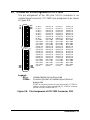
2.7 Connector Pin Assignment of PCI-7433
The pin assignment of the 100 pins SCSI-II connector is an
isolated signal connector, PCI-7433’s pin assignment is as shown
in Figure 2.8.
(1)
(2)
(3)
(52)
(53)
(51)
(48)
(49)
(50)
(98)
(99)
(100)
Legend:
IDI_n : Isolated digital input channel #n
COMm : Common junction of isolated input channel
groupp #m
(COM1 is common junction of input channel #0~7, COM2 is
common junction of input channel #8~15, COM3 is common
junction of input channel #16~15, … )
Figure 2.8. Pin Assignment of PCI-7433 Connector CN1
(1) IDI_0 (26) IDI_32 (51) IDI_8 (76) IDI_40
(2) IDI_1 (27) IDI_33 (52) IDI_9 (77) IDI_41
(3) IDI_2 (28) IDI_34 (53) IDI_10 (78) IDI_42
(4) IDI_3 (29) IDI_35 (54) IDI_11 (79) IDI_43
(5) IDI_4 (30) IDI_36 (55) IDI_12 (80) IDI_44
(6) IDI_5 (31) IDI_37 (56) IDI_13 (81) IDI_45
(7) IDI_6 (32) IDI_38 (57) IDI_14 (82) IDI_46
(8) IDI_7 (33) IDI_39 (58) IDI_15 (83) IDI_47
(9) COM1 (34) COM5 (59) COM2 (84) COM6
(10) COM1 (35) COM5 (60) COM2 (85) COM6
(11) COM1 (36) COM5 (61) COM2 (86) COM6
(12) COM1 (37) COM5 (62) COM2 (87) COM6
(13) IDI_16 (38) IDI_48 (63) IDI_24 (88) IDI_56
(14) IDI_17 (39) IDI_49 (64) IDI_25 (89) IDI_57
(15) IDI_18 (40) IDI_50 (65) IDI_26 (90) IDI_58
(16) IDI_19 (41) IDI_51 (66) IDI_27 (91) IDI_59
(17) IDI_20 (42) IDI_52 (67) IDI_28 (92) IDI_60
(18) IDI_21 (43) IDI_53 (68) IDI_29 (93) IDI_61
(19) IDI_22 (44) IDI_54 (69) IDI_30 (94) IDI_62
(20) IDI_23 (45) IDI_55 (70) IDI_31 (95) IDI_63
(21) COM3 (46) COM7 (71) COM4 (96) COM8
(22) COM3 (47) COM7 (72) COM4 (97) COM8
(23) COM3 (48) COM7 (73) COM4 (98) COM8
(24) COM3 (49) COM7 (74) COM4 (99) COM8
(25) NC (50) NC (75) NC (100) NC

12 •• Installation
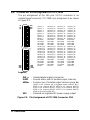
2.8 Connector Pin Assignment of PCI-7434
The pin assignment of the 100 pins SCSI-II connector is an
isolated signal connector, PCI-7434’s pin assignment is as shown
in Figure 2.9.
(1)
(2)
(3)
(52)
(53)
(51)
(48)
(49)
(50)
(98)
(99)
(100)
Legend:
IDO_n : Isolated digital output channel #n
IGND : Ground return path of isolated output channels
VDDm : Common pin of isolated output channel group #m
(VDD1 is the common pin of isolated output channel #0~7,
VDD2 is for channel #8~15, VDD3 is for channel #16~23,
VDD4 is for channel #24~31, VDD5 is for channel #32~39,
VDD6 is for channel #40~47, VDD7 is for channel #48~55,
VDD8 is for channel #56~63 )
V5V : Onboard un-regulated 5V power supply output
Figure 2.9. Pin Assignment of PCI-7434 Connector CN1
(1) IDO_0 (26) IDO_32 (51) IDO_8 (76) IDO_40
(2) IDO_1 (27) IDO_33 (52) IDO_9 (77) IDO_41
(3) IDO_2 (28) IDO_34 (53) IDO_10 (78) IDO_42
(4) IDO_3 (29) IDO_35 (54) IDO_11 (79) IDO_43
(5) IDO_4 (30) IDO_36 (55) IDO_12 (80) IDO_44
(6) IDO_5 (31) IDO_37 (56) IDO_13 (81) IDO_45
(7) IDO_6 (32) IDO_38 (57) IDO_14 (82) IDO_46
(8) IDO_7 (33) IDO_39 (58) IDO_15 (83) IDO_47
(9) VDD1 (34) VDD5 (59) VDD2 (84) VDD6
(10) IGND (35) IGND (60) IGND (85) IGND
(11) IGND (36) IGND (61) IGND (86) IGND
(12) IGND (37) IGND (62) IGND (87) IGND
(13) IDO_16 (38) IDO_48 (63) IDO_24 (88) IDO_56
(14) IDO_17 (39) IDO_49 (64) IDO_25 (89) IDO_57
(15) IDO_18 (40) IDO_50 (65) IDO_26 (90) IDO_58
(16) IDO_19 (41) IDO_51 (66) IDO_27 (91) IDO_59
(17) IDO_20 (42) IDO_52 (67) IDO_28 (92) IDO_60
(18) IDO_21 (43) IDO_53 (68) IDO_29 (93) IDO_61
(19) IDO_22 (44) IDO_54 (69) IDO_30 (94) IDO_62
(20) IDO_23 (45) IDO_55 (70) IDO_31 (95) IDO_63
(21) VDD3 (46) VDD7 (71) VDD4 (96) VDD8
(22) IGND (47) IGND (72) IGND (97) IGND
(23) IGND (48) IGND (73) IGND (98) IGND
(24) IGND (49) IGND (74) IGND (99) IGND
(25) NC (50) V5V (75) NC (100) V5V

Register Structure & Connection •• 13
3
Register Format &Register Format &
ConnectionConnection
In this chapter, a primitive digital I/O operations of PCI-743X
products will be specified. The I/O operations are also included.
3.1 I/O Port Base Address
The PCI-743X or cPCI-743X function as a 32-bit PCI target
(slave) device to any master on the PCI bus. There are three
types of registers on the PCI-743X: PCI Configuration Registers
(PCR), Local Configuration Registers (LCR) and PCI-743X
registers.
The PCR which conforms the PCI-bus specifications is initialized
and controlled by the system plug & play PCI BIOS. User‘s can
refer to the PCI BIOS specification to understand how to get
information from the PCR.
The LCR is specified by the PCI bus controller PLX-9050. It is not
necessary for users to understand the details of the LCR if you
use the software library. The base address of the LCR is
assigned by the PCI PnP BIOS. The assigned address is located
at offset 14h of PCR. Please refer to the PCI-9050’s data sheet
for the detail operation of the LCR and also the register format of
the PCR.
The PCI-743X registers are shown in the Table 3.1. The base
address of the PCI-743X registers is also assigned by the PCI

14 •• Register Structure & Connection
PnP BIOS. The assigned base address is located at offset 18h of
PCR. Therefore, users can read the PCR to know the base
address by using the BIOS function call. Note that the PCI-743X
registers are all 32 bits. The users can access these registers by
32 bits I/O instructions.
3.2 Registers Map
The PCI-7432 board requires 4 consecutive 8-bit addresses (32-
bit) in the PC I/O address space. The PCI-7433 and 7434
requires 8 consecutive addresses (32-bit) in the PC I/O address
space. Table 3.1 shows the I/O address of each register with
respect to the base address.
Address Write Read
PCI-7432
Base (0 - 3 ) Isolated DO Isolated DI
PCI-7433
Base (0 - 7 ) -- Isolated DI
PCI-7434
Base (0 - 7 ) Isolated DO --
Table 3.1. I/O Address Map of PCI-7432/33/34
DO -- Digital Output
DI -- Digital Input
Caution :
1. I/O port is 32-bit width
2. 8-bit or 16-bit I/O access is not allowed.
3.2 Digital Input Register
There are 32 isolated digital input channels on PCI-7432 and 64
isolated digital input channels on the PCI-7433, each bit of based
address is corresponding to a signal on the digital input channel.
Address :
BASE + 0 ~ BASE + 3 for 7432
BASE + 0 ~ BASE + 7 for 7433
Attribute: read only
Data Format :

Register Structure & Connection •• 15
PCI-7432
7 6 5 4 3 2 1 0
Base + 0 IDI_7 IDI_6 IDI_5 IDI_4 IDI_3 IDI_2 IDI_1 IDI_0
Base + 1 IDI_15 IDI_14 IDI_13 IDI_12 IDI_11 IDI_10 IDI_9 IDI_8
Base + 2 IDI_23 IDI_22 IDI_21 IDI_20 IDI_19 IDI_18 IDI_17 IDI_16
Base + 3 IDI_31 IDI_30 IDI_29 IDI_28 IDI_27 IDI_26 IDI_25 IDI_24
PCI-7433
7 6 5 4 3 2 1 0
Base + 0 IDI_7 IDI_6 IDI_5 IDI_4 IDI_3 IDI_2 IDI_1 IDI_0
Base + 1 IDI_15 IDI_14 IDI_13 IDI_12 IDI_11 IDI_10 IDI_9 IDI_8
Base + 2 IDI_23 IDI_22 IDI_21 IDI_20 IDI_19 IDI_18 IDI_17 IDI_16
Base + 3 IDI_31 IDI_30 IDI_29 IDI_28 IDI_27 IDI_26 IDI_25 IDI_24
Base + 4 IDI_39 IDI_38 IDI_37 IDI_36 IDI_35 IDI_34 IDI_33 IDI_32
Base + 5 IDI_47 IDI_46 IDI_45 IDI_44 IDI_43 IDI_42 IDI_41 IDI_40
Base + 6 IDI_55 IDI_54 IDI_53 IDI_52 IDI_51 IDI_50 IDI_49 IDI_48
Base + 7 IDI_63 IDI_62 IDI_61 IDI_60 IDI_59 IDI_58 IDI_57 IDI_56
IDI_N : Isolated Digital Input CH N
3.3 Digital Output Register
There are total 32 digital output channels on the PCI-7432 and 64
isolated digital input channels on the PCI-7434, each bit of based
address is corresponding to a signal on the digital output
channel.
Address: BASE + 0 ~ BASE + 3 for 7432
BASE + 0 ~ BASE + 7 for 7434
Attribute: write only
Data Format :
PCI-7432
7 6 5 4 3 2 1 0
Base + 0
IDO_7 IDO_6 IDO_5 IDO_4 IDO_3 IDO_2 IDO_1 IDO_0
Base + 1
IDO_15 IDO_14 IDO_13 IDO_12 IDO_11 IDO_10 IDO_9 IDO_8
Base + 2
IDO_23 IDO_22 IDO_21 IDO_20 IDO_19 IDO_18 IDO_17 IDO_16
Base + 3
IDO_31 IDO_30 IDO_29 IDO_28 IDO_27 IDO_26 IDO_25 IDO_24
PCI-7434
7 6 5 4 3 2 1 0
Base + 0
IDO_7 IDO_6 IDO_5 IDO_4 IDO_3 IDO_2 IDO_1 IDO_0
Base + 1
IDO_15 IDO_14 IDO_13 IDO_12 IDO_11 IDO_10 IDO_9 IDO_8
Page is loading ...
Page is loading ...
Page is loading ...
Page is loading ...
Page is loading ...
Page is loading ...
Page is loading ...
Page is loading ...
Page is loading ...
Page is loading ...
Page is loading ...
Page is loading ...
Page is loading ...
Page is loading ...
Page is loading ...
Page is loading ...
-
 1
1
-
 2
2
-
 3
3
-
 4
4
-
 5
5
-
 6
6
-
 7
7
-
 8
8
-
 9
9
-
 10
10
-
 11
11
-
 12
12
-
 13
13
-
 14
14
-
 15
15
-
 16
16
-
 17
17
-
 18
18
-
 19
19
-
 20
20
-
 21
21
-
 22
22
-
 23
23
-
 24
24
-
 25
25
-
 26
26
-
 27
27
-
 28
28
-
 29
29
-
 30
30
-
 31
31
-
 32
32
-
 33
33
-
 34
34
-
 35
35
-
 36
36


ADLINK Technology cPCI-7433 User manual
- Type
- User manual
Ask a question and I''ll find the answer in the document
Finding information in a document is now easier with AI
Related papers
-
ADLINK Technology pci-6308 User manual
-
-
-
Adlink PCI-7230/33/34 User manual
-
-
Adlink NuDAQ PCI-6208A User manual
-
-
-
-
Other documents
-
CH Tech M/MA Module Carrier AMi3000 User manual
-
-
ESD CPCI-COM4 Owner's manual
-
-
-
Parker Hannifin acr-motion max api User manual
-
ICP PCI-D64HU User manual
-
 Meilhaus Electronic ME-94 PCI User manual
-
Hafele 422.29.350 Operating instructions
-
 Buddy Products 7434-4 Operating instructions

