Texas Instruments A to Voltage Translation With TXB-Type Translators Application Note
- Category
- Voltage regulators
- Type
- Application Note
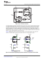
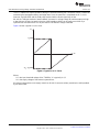
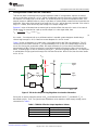
Texas Instruments A to Voltage Translation With TXB-Type Translators help remedy many problems in system voltage compatibility. Due to not requiring a DIR control signal and each channel supporting independent transmission or reception of data, they eliminate the need for a processor GPIO to control a DIR input, resulting in simplified software driver development as well as smaller device packaging due to reduced pin-count. The TXB010x devices are intended for use in push-pull CMOS driver applications such as Secure Digital (SD) or Serial Peripheral Interface (SPI).
Texas Instruments A to Voltage Translation With TXB-Type Translators help remedy many problems in system voltage compatibility. Due to not requiring a DIR control signal and each channel supporting independent transmission or reception of data, they eliminate the need for a processor GPIO to control a DIR input, resulting in simplified software driver development as well as smaller device packaging due to reduced pin-count. The TXB010x devices are intended for use in push-pull CMOS driver applications such as Secure Digital (SD) or Serial Peripheral Interface (SPI).


-
 1
1
-
 2
2
-
 3
3
-
 4
4
-
 5
5
-
 6
6
-
 7
7


Texas Instruments A to Voltage Translation With TXB-Type Translators Application Note
- Category
- Voltage regulators
- Type
- Application Note
Texas Instruments A to Voltage Translation With TXB-Type Translators help remedy many problems in system voltage compatibility. Due to not requiring a DIR control signal and each channel supporting independent transmission or reception of data, they eliminate the need for a processor GPIO to control a DIR input, resulting in simplified software driver development as well as smaller device packaging due to reduced pin-count. The TXB010x devices are intended for use in push-pull CMOS driver applications such as Secure Digital (SD) or Serial Peripheral Interface (SPI).
Ask a question and I''ll find the answer in the document
Finding information in a document is now easier with AI
Related papers
-
Texas Instruments Differences between PCM270x and PCM270xC Application notes
-
-
-
-
-
-
Texas Instruments 4Q User manual
-
-
-