Page is loading ...

7/30/2019 Basys MX3 Reference Manual [Reference.Digilentinc]
https://reference.digilentinc.com/reference/microprocessor/basys-mx3/reference-manual?_ga=2.68739409.1349070004.1564406803-1961480359.1
…
1/52
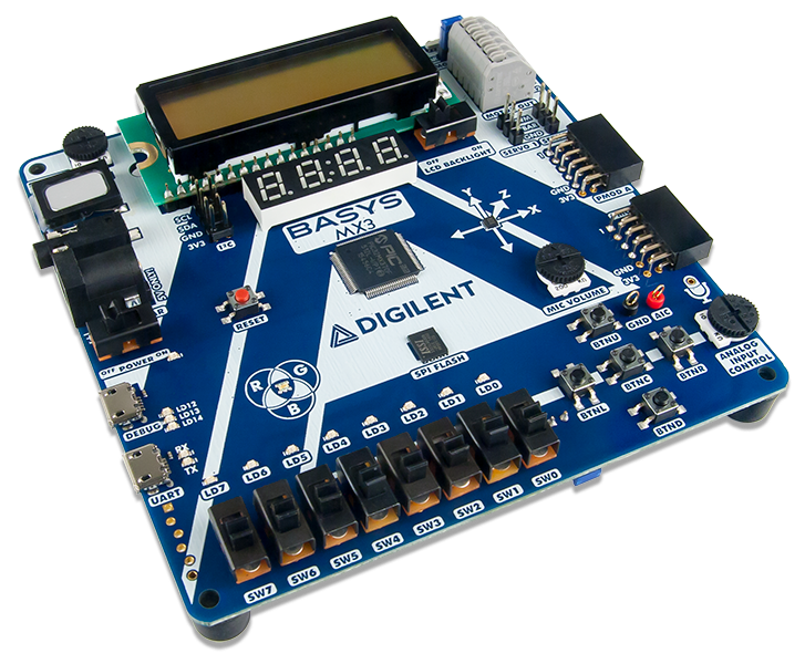
The Basys MX3 is a true MCU trainer board designed from the ground up around the teaching experience. Basys MX3 features the
PIC32MX370 from Microchip and was designed to be used with the MPLAB® X IDE. With an exhaustive set of peripherals, students gain
exposure to a wide range of embedded systems related concepts while using a professional grade tool set. Accompanied by free and open
source coursework, including seven in-depth teaching units and 15 complete labs, the Basys MX3 is a versatile MCU trainer board ideal for
teaching introductory embedded systems courses.
(https://reference.digilentinc.com/_media/reference/microprocessor/basys-mx3/basysmx3-0.png)
Basys MX3 Reference Manual

7/30/2019 Basys MX3 Reference Manual [Reference.Digilentinc]
https://reference.digilentinc.com/reference/microprocessor/basys-mx3/reference-manual?_ga=2.68739409.1349070004.1564406803-1961480359.1
…
2/52

7/30/2019 Basys MX3 Reference Manual [Reference.Digilentinc]
https://reference.digilentinc.com/reference/microprocessor/basys-mx3/reference-manual?_ga=2.68739409.1349070004.1564406803-1961480359.1
…
3/52

7/30/2019 Basys MX3 Reference Manual [Reference.Digilentinc]
https://reference.digilentinc.com/reference/microprocessor/basys-mx3/reference-manual?_ga=2.68739409.1349070004.1564406803-1961480359.1
…
4/52

7/30/2019 Basys MX3 Reference Manual [Reference.Digilentinc]
https://reference.digilentinc.com/reference/microprocessor/basys-mx3/reference-manual?_ga=2.68739409.1349070004.1564406803-1961480359.1
…
5/52
Basys MX3 PDF (https://reference.digilentinc.com/_media/reference/microprocessor/basys-mx3/basys_mx3_rm.pdf)
PIC32MX370F512L Microcontroller
MIPS32® M4K® core runs up to 96 MHz () using onboard 8 MHz () oscillator
512 KB of Program Flash Memory, 12 KB of Boot Flash Memory
128 KB of SRAM
Four Direct Memory Access (DMA) Modules
Two SPI, Two I²C, and Five UART serial interfaces
Parallel Master Port (PMP) for graphics interfaces
Five 16-bit Timers/Counters
Five Input Capture Modules
Five Output Compare Modules
85 I/O pins
54 pins support Peripheral Pin Select (PPS) for function remapping
Power
Powered from USB or any 5V external power source
USB and Debugging
USB-UART Bridge
USB programmer/debugger
30-pin Analog Discovery 2 connector
Download This Reference Manual
Features

7/30/2019 Basys MX3 Reference Manual [Reference.Digilentinc]
https://reference.digilentinc.com/reference/microprocessor/basys-mx3/reference-manual?_ga=2.68739409.1349070004.1564406803-1961480359.1
…
6/52
Switches, Push-buttons, LEDs and Displays
5 Push-buttons
1 Reset button
8 Slide switches
8 LEDs
1 RGB LED ()
4 Digit 7-segment display
LCD () character display
Audio, Motor control, and other devices
Speaker with Audio Output Jack and volume control
Microphone with volume control
Dual H-Bridge Motor Driver for up to two 1.5 A Brushed DC Motors or one stepper motor
2 Servo Connectors
FIR-compatible IrDA Module
Potentiometer
3-axis, 12-bit accelerometer
4 MB () SPI Flash
Expansion Connectors
Two standard Pmod ports
16 Total microcontroller I/O
One I2C Connector
2 Total microcontroller I/O
(https://reference.digilentinc.com/_detail/reference/microprocessor/basys-mx3/basys_mx3_walkaround.png?
id=reference%3Amicroprocessor%3Abasys-mx3%3Areference-manual) (https://reference.digilentinc.com/_detail/reference/microprocessor/basys-
mx3/basysmx3_-_bottom.png?id=reference%3Amicroprocessor%3Abasys-mx3%3Areference-manual)

7/30/2019 Basys MX3 Reference Manual [Reference.Digilentinc]
https://reference.digilentinc.com/reference/microprocessor/basys-mx3/reference-manual?_ga=2.68739409.1349070004.1564406803-1961480359.1
…
7/52
The Basys MX3 is fully supported by Microchip’s MPLAB X IDE. See section 1 on Programming the Board for more information on using
the Basys MX3 in MPLAB X IDE. Digilent provides a set of libraries called the Basys MX3 Library Pack that adds support for all onboard
peripherals. This library pack can be downloaded from the Basys MX3 Resource Center
(https://reference.digilentinc.com/reference/microprocessor/basys-mx3/start). The users may choose to implement their own functionality in
order to access Basys MX3 resources.
The Basys MX3 can also be used in Arduino IDE once the Digilent Core for Arduino IDE has been installed. Instructions for installing the
Digilent Core for Arduino IDE can be found on the Basys MX3 Resource Center.
Basys MX3 comes with a complete set of coursework designed to give teaching professionals flexibility in designing embedded systems and
other microprocessor courses. With almost 300 pages of material, “Embedded Systems Basys MX3 and PIC32MX370” covers topics from
toggling LEDs, motor control, and introduction to digital signal processing. Access to the full coursework is available on the Basys MX3
Resource Center.
Links to additional materials from Digilent and Microchip, including the Basys MX3 schematic and the PIC32MX370F512L datasheet, can
also be found on the Basys MX3 Resource Center.
The Basys MX3 uses a lot of devices to implement all of the functionality it provides (accelerometer, flash memory, motor driver, IRDA,
etc.). The manufacturers of each of these devices provide detailed descriptions of their functionality in their datasheets.
The Basys MX3 can be used with Microchip’s standard MPLAB X IDE. This software suite can be downloaded for free from the Microchip
website and includes a free evaluation copy of the XC32 compiler for use with the PIC32 microcontroller family.
MPLAB X IDE is the tool used to write, compile, program, and debug code running on the Basys MX3 board. Programming and
debugging a program on the Basys MX3 using the MPLAB X IDE is possible using the DEBUG USB connector. The board contains all
the required circuitry for MPLAB X to communicate with the onboard PIC32, so no additional programming tools need to be purchased.
When creating a new project in MPLAB X, a wizard allows you to setup the environment and device specific tools. The steps for this
include the following:
1. Select Microchip Embedded / Standalone Project, then use the “Select Device” option to specify the PIC32 microcontroller being
used: PIC32MX370F512L.
Software Support
Coursework and Additional Materials
1. Programming the Board
1.1. Programming Tools

7/30/2019 Basys MX3 Reference Manual [Reference.Digilentinc]
https://reference.digilentinc.com/reference/microprocessor/basys-mx3/reference-manual?_ga=2.68739409.1349070004.1564406803-1961480359.1
…
8/52
2. Select the programming tool named Basys MX3 corresponding to the board you want to program, under Licensed Debugger group.
3. Select the compiler you want to use.
Another useful tool included with MPLAB X is MPLAB X IPE. This tool allows the direct programming/erasing of the microcontroller,
but it does not provide an environment for writing, compiling, and debugging the code. Please see Microchip documentation for
instructions on using this tool.
It is often very helpful to include the xc.h header when writing code for the Basys MX3:
#include <xc.h>
This further provides the inclusion of another header (p32mx370f512l.h) into the project that provides useful definitions such as:
Register names
example (register LATA is set to 0):
LATA = 0;
Specific register bits that can be accessed using a structure having the name of the register suffixed by “bits”.
1.2. Programming Basics

7/30/2019 Basys MX3 Reference Manual [Reference.Digilentinc]
https://reference.digilentinc.com/reference/microprocessor/basys-mx3/reference-manual?_ga=2.68739409.1349070004.1564406803-1961480359.1
…
9/52
example (bit LATA1 of the register LATA is set to 1):
LATAbits.LATA1 = 1;
Digilent provides a set of libraries called the Basys MX3 Library Pack that addresses much of the functionality on the Basys MX3:
ACL () (accelerometer)
ADC () (Analog to Digital converter)
AUDIO
BTN (buttons)
IRDA
LCD ()
LED ()
MIC (microphone)
MOT (motors)
PMODS
RGBLED
SPIFLASH
SSD ()
SWT (Switches)
UART
These libraries are wrappers over the lower level functions that access the registers, allowing the user to call the functionality using functions
like:
LED_Init();
LED_SetValue(4, 1); //turn on LED4
This set of libraries comes with the user documentation, but basically this is what you have to do in order to use them:
Include in your project the .c and .h files corresponding to the module you want to use (for example led.c and led.h).
In your code, include the header of the module:
#include "led.h"
In your code, call the needed functions
The PIC32MX370F512L microcontroller offers access to all the board resources through its pins, so understanding how to access their
features is very important. The list that describes each pin functionality is included in Appendix 3. You can see that each pin may have
multiple functions, but all pins have one feature in common: they have an associated digital I/O (input/output) bit. On PIC32
microcontrollers, the I/O pins are grouped into I/O Ports and are accessed via peripheral registers in the microcontroller. There are seven
I/O Ports numbered A–G and each is 16 bits wide. Depending on the PIC32 microcontroller, some of the I/O Ports are not present, and
not all 16 bits are accessible in all I/O Ports.
Each I/O Port has the following control registers: TRIS, LAT, PORT, ANSEL, CNPU, CNPD, and ODC. The registers for each I/O Port
are named after it: TRISx, LATx, PORTx, ANSELx, CNPUx, CNPDx and ODCx. For example, port A will have the following assigned
registers: TRISA, LATA, etc.
The TRIS register is used to set the pin direction. Setting a TRIS bit to 0 makes the corresponding pin an output. Setting the TRIS bit to 1
makes the pin an input.
The LAT register is used to write to the I/O Port. Writing to the LAT register sets any pins configured as outputs. Reading from the LAT
register returns the last value written.
The PORT register is used to read from the I/O Port. Reading from the PORT register returns the current state of all the pins in the I/O
Port. Writing to the PORT register may not produce the expected result, therefore writing to LAT register is recommended.
To summarize: write using LAT, read using PORT.
PIC32 microcontrollers allow any pin set as an output to be configured as either a normal digital output or as an open-drain output. The
ODC register is used to control the output type. Setting an ODC bit to 0 makes the pin a normal output and setting it to 1 makes the pin an
open-drain output.
The multifunction pins that include analog input functionality need to be configured in order to be used as digital pins by clearing the
corresponding bit from ANSEL register. These pins will include ANx in their name. For example: AN11/PMA12/RB11 for RB11.
1.3. Digital Inputs and Outputs

7/30/2019 Basys MX3 Reference Manual [Reference.Digilentinc]
https://reference.digilentinc.com/reference/microprocessor/basys-mx3/reference-manual?_ga=2.68739409.1349070004.1564406803-1961480359.
…
10/52
This microcontroller has a weak pull-up and a weak pull-down connected to each pin. These pull-ups and pull-downs are enabled/disabled
by setting the corresponding bits from CNPU and CNPD registers to 1/0. The default setting is 0 (pull-ups and pull-downs disabled).
You can see a typical example of I/O pin configuration as output and digital output operations in the User LEDs section.
You can see a typical example of I/O pin configuration as input (including analog disable) and digital input operations in the User Buttons
section.
Refer to the PIC32MX3XX/4XX Family Datasheet, and the PIC32 Family Reference Manual, Section 12, IO Ports, for more detailed
information about the operation of the I/O Ports in the microcontroller.
Users may independently map the input and/or output of most digital peripherals to a fixed subset of digital I/O pins. Pins that support the
peripheral pin select feature include the designation “RPn” in their full pin designation, where “RP” designates a remappable peripheral and
“n” is the remappable port number.
The available peripherals to be mapped are digital-only. These include general serial communications (UART and SPI), general purpose
timer clock inputs, timer-related peripherals (input capture and output compare), and interrupt-on-change inputs.
On the other hand, some peripheral modules cannot be included in the peripheral pin select feature because it requires special I/O circuitry
on a specific port and it cannot be easily connected to multiple pins. These modules include I2C and analog-to-digital converters (ADC ()),
among others.
Peripheral pin select features are controlled using two sets of Special Function Registers (SFRs): one to map peripheral inputs, and one to
map peripheral outputs.
The peripheral inputs are mapped and named from the peripheral perspective (based on the peripheral). The [pin name]R registers, where
[pin name] refers to the specific peripheral pins, are used to configure peripheral input mapping. TABLE 12-1 in the PIC32MX370F512L
datasheet from Microchip (and Appendix 1 in this document) shows the different pins and their values available to assign to a peripheral pin.
The following example shows how different I/Os, such as pin RF4, can be assigned to U1RX input pin of the UART1 peripheral:
U1RXR = 0x02; // 0010 corresponds to RF4
The peripheral outputs are mapped and named from the pin perspective (on the basis of the pin). The RPnR registers (Register 12-2) are
used to control output mapping. The PIC32MX370F512L datasheet details in TABLE 12-2 (and Appendix 2 in this document) the values
corresponding to each IO pin, associated to each available peripheral pin. Note that the current version of the Basys MX3 schematic (B.0)
incorrectly lists RD6 and RD7 as remappable pins (RPD6 and RPD7, respectively); these pins are not remappable on the
PIC32MX370F512L.
The following example shows how different peripheral outputs, such as U3TX, can be assigned to pin RF4:
RPF4R = 0x01; // 0001 corresponds to U3TX
1.4. Remappable pins

7/30/2019 Basys MX3 Reference Manual [Reference.Digilentinc]
https://reference.digilentinc.com/reference/microprocessor/basys-mx3/reference-manual?_ga=2.68739409.1349070004.1564406803-1961480359.1
…
11/52
Input and output remapping is illustrated in the SPI2 section, where the SPI2 pins are mapped over the pins of PMOD A connector.
The PIC32 microcontroller supports numerous clock source options for the main processor operating clock. The Basys MX3 uses an 8MHz
external crystal for use with the XT oscillator option. Oscillator options are selected via the configuration settings specified using the
#pragma config
statement. Use
#pragma config POSCMOD=XT
to select the XT option.
Using the internal system clock phase-locked loop (PLL), it is possible to select numerous multiples or divisions of the 8MHz oscillator to
produce CPU operating frequencies up to 80MHz. The clock circuit PLL provides an input divider, multiplier, and output divider. The
external clock frequency (8MHz) is first divided by the input divider value selected. This is multiplied by the selected multiplier value and
then finally divided by the selected output divider. The result is the system clock, SYSCLK, frequency. The SYSCLK frequency is used by
the CPU, DMA controller, interrupt controller, and pre-fetch cache.
The values controlling the operating frequency are specified using the PIC32MX370 configuration variables. These are set using the
#pragma config statement. Use
#pragma config FPLLIDIV
to set the input divider,
#pragma config FPLLMUL
to set the multiplication factor and
#pragma config FPLLODIV
to set the output divider. Refer to the PIC32MX3XX/4XX Family Data Sheet and the PIC32MX Family Reference Manual, Section
Oscillators, for information on how to choose the correct values, as not all combinations of multiplication and division factors will work.
In addition to configuring the SYSCLK frequency, the peripheral bus clock, PBCLK, frequency is also configurable. The peripheral bus
clock is used for most peripheral devices, and in particular is the clock used by the timers, and serial controllers (UART, SPI, I2C). The
PBLCK frequency is a division of the SYSCLK frequency selected using
#pragma config FPBDIV
The PBCLK divider can be set to divide by 1, 2, 4, or 8.
The following example will set up the Basys MX3 for operation with a SYSCLK frequency of 80MHz and a PBCLK frequency of 80MHz.
1.5. CPU Clock Source

7/30/2019 Basys MX3 Reference Manual [Reference.Digilentinc]
https://reference.digilentinc.com/reference/microprocessor/basys-mx3/reference-manual?_ga=2.68739409.1349070004.1564406803-1961480359.
…
12/52
#pragma config FNOSC = FRCPLL
#pragma config FSOSCEN = OFF
#pragma config POSCMOD = XT
#pragma config OSCIOFNC = ON
#pragma config FPBDIV = DIV_1
#pragma config FPLLIDIV = DIV_2
#pragma config FPLLMUL = MUL_20
#pragma config FPLLODIV = DIV_1
The Basys MX3 requires a 5-volt power source to operate. This power source can come from the Programming / Debugging USB port
(J12), the USB-UART (J10), or from an external 5 Volt DC power supply that’s connected to Power Jack (J11). These three power inputs are
connected together through Schottky diodes to form the primary input power network, VIN, which is used to power the onboard regulators
and the majority of the onboard peripherals. No jumper is required to select the input power source. The board will automatically power on
while the Power Switch (SW8) is in the on position and power is present on any of the power inputs.
A power-good LED () (LD11), driven by the output of the 3.3 volt regulator (LMR10515), indicates that the board is receiving power and
that the on-board supplies are functioning as expected. An overview of the Basys MX3 power circuit is shown in Fig. 2.1.
The USB port(s) can deliver enough power for the vast majority of designs. However, a few demanding applications, including any that drive
multiple peripheral boards, may require more power than a USB port is capable of providing. In these instances an external power supply
can be used. Due to their high current demands motors and servos cannot be powered through either of the USB ports, and may only be
powered through an external supply.
An external power supply can be used by plugging into Power Jack J11. The supply must use a coaxial, center-positive 2.0 mm internal-
diameter plug, and provide a voltage of 5 Volts DC (4.75 Volts minimum, 5.5 Volts maximum). The supply should provide a minimum
current of 2 amps if servos are to be used. Ideally, the supply should be capable of provide 20 Watts of power (5 Volts DC, 4 amps). Many
suitable supplies can be purchased from Digilent or other catalog vendors.
2. Power Supplies

7/30/2019 Basys MX3 Reference Manual [Reference.Digilentinc]
https://reference.digilentinc.com/reference/microprocessor/basys-mx3/reference-manual?_ga=2.68739409.1349070004.1564406803-1961480359.
…
13/52
The on-board Motor Driver (Texas Instruments DRV8835) may be powered by a 5 Volt supply connected to Power Jack J11 or by an
external supply (0 Volts to 11 Volts) connected to pins 1 and 2 of Terminal Block J5. Jumper JP1 is used to select which power source is
used by the Motor Driver.
Table 2.1. Power rail characteristics.
Supply Circuit Device
Current
(max/typical)
3.3V
(VCC3V3)
PIC32MX370, Pmods, and all on-board peripherals excluding the LCD ()
backlight, RGB LED (), IrDA LED (), Servos, and Motors
IC10: Texas
Instruments
LMR10515
1.5A/NA
3.3V
(DBG3V3)
Onboard Microchip Programmer/Debugger IC11: Texas
Instruments
LP2985IM5-3.3
150mA/NA
Eight LEDs are provided, labeled LD0 – LD7 on the board (and LED0 – LED7 on the schematic), attached to eight digital IO pins.
Controlling the LEDs is done by basic access to an output IO pin. Read more details in the Digital Inputs and Outputs chapter.
Figure 3.1 shows the way the LEDs are electrically connected on the Basys MX3.
Table 3.1. LED () connectivity.
Label Schematic Name PIC32 Pin Description
LD0 LED0 TMS/CTED1/RA0 Led 0
LD1 LED1 TCK/CTED2/RA1 Led 1
3. User LEDs
3.1. Connectivity

7/30/2019 Basys MX3 Reference Manual [Reference.Digilentinc]
https://reference.digilentinc.com/reference/microprocessor/basys-mx3/reference-manual?_ga=2.68739409.1349070004.1564406803-1961480359.
…
14/52
Label Schematic Name PIC32 Pin Description
LD2 LED2 SCL2/RA2 Led 2
LD3 LED3 SDA2/RA3 Led 3
LD4 LED4 TDI/CTED9/RA4 Led 4
LD5 LED5 TDO/RA5 Led 5
LD6 LED6 TRCLK/RA6 Led 6
LD7 LED7 TRD3/CTED8/RA7 Led 7
All the pins must be defined as digital output (their corresponding TRIS bit must be set to 0):
TRISAbits.TRISA<0-7> = 0; // LED<0-7> configured as output
In order to turn an LED () on or off, turn the corresponding digital output pin high or low by writing 1 or 0 to the corresponding LATA
register bit.
LATAbits.LATA<0-7> = 1; // turn led on
or
LATAbits.LATA<0-7> = 0; // turn led off
Library functions for using the LEDs are contained in the Basys MX3 library pack, LED () library. However, the user can easily use the
LEDs without the LED () library, as presented above.
Eight switches are provided, labeled SW0 – SW7 on the board and in the schematic, attached to eight digital IO pins of the PIC32. Reading
the switches is done by basic access to an input IO pin. Read more details in Digital Inputs and Outputs chapter.
Figure 4.1 shows the way the switches are electrically connected on the Basys MX3.
3.2. Functionality
4. User Switches

7/30/2019 Basys MX3 Reference Manual [Reference.Digilentinc]
https://reference.digilentinc.com/reference/microprocessor/basys-mx3/reference-manual?_ga=2.68739409.1349070004.1564406803-1961480359.
…
15/52
Table 4.1. Switches connectivity.
Label Schematic Name PIC32 Pin Pin Shared With Description
SW0 SW0 RPF3/RF3 Switch 0
SW1 SW1 RPF5/PMA8/RF5 Switch 1
SW2 SW2 RPF4/PMA9/RF4 Switch 2
SW3 SW3 RPD15/RD15 Switch 3
SW4 SW4 RPD14/RD14 Switch 4
SW5 SW5 AN11/PMA12/RB11 Switch 5
SW6 SW6 CVREFOUT/AN10/RPB10/CTED11PMA13/RB10 Switch 6
SW7 SW7 AN9/RPB9/CTED4/RB9 TRIG_2 Switch 7
All the pins must be defined as digital input: their corresponding TRIS bit must be set to 1, and analog function must be disabled for pins
routed to SW5, SW6 and SW7.
TRISFbits.TRISF3 = 1; // RF3 (SW0) configured as input
TRISFbits.TRISF5 = 1; // RF5 (SW1) configured as input
TRISFbits.TRISF4 = 1; // RF4 (SW2) configured as input
TRISDbits.TRISD15 = 1; // RD15 (SW3) configured as input
TRISDbits.TRISD14 = 1; // RD14 (SW4) configured as input
TRISBbits.TRISB11 = 1; // RB11 (SW5) configured as input
ANSELBbits.ANSB11 = 0; // RB11 (SW5) disabled analog
TRISBbits.TRISB10 = 1; // RB10 (SW6) configured as input
ANSELBbits.ANSB10 = 0; // RB10 (SW6) disabled analog
TRISBbits.TRISB9 = 1; // RB9 (SW7) configured as input
ANSELBbits.ANSB9 = 0; // RB9 (SW7) disabled analog
In order to read the switches, the user needs to read the corresponding digital input pin. A value of 1 indicates the switch as being on (high)
or 0 indicates the switch as being off (low).
val = PORTFbits.RF3; // read SW0
val = PORTFbits.RF5; // read SW1
val = PORTFbits.RF4; // read SW2
val = PORTDbits.RD15; // read SW3
val = PORTDbits.RD14; // read SW4
val = PORTBbits.RB11; // read SW5
val = PORTBbits.RB10; // read SW6
val = PORTBbits.RB9; // read SW7
4.1. Connectivity
4.2. Functionality

7/30/2019 Basys MX3 Reference Manual [Reference.Digilentinc]
https://reference.digilentinc.com/reference/microprocessor/basys-mx3/reference-manual?_ga=2.68739409.1349070004.1564406803-1961480359.
…
16/52
Library functions for using the switches are contained in the Basys MX3 library pack, SWT library. However, the user can easily use the
switches without the SWT library, as presented above.
As shown in the connectivity table above, SW7 driving signal is shared with the TRIG_2 signal in 2×15 Pins Debug Header.
There are five buttons on the board, labeled BTNU, BTNL, BTNC, BTNR, BTND both on the board and in the schematic, attached to five
digital IO pins of PIC32. Reading the buttons is done by basic access to an input IO pin. Read more details in Digital Inputs and Outputs
chapter.
Figure 5.1 shows the way the buttons are electrically connected on the Basys MX3.
Table 5.1. Button connectivity.
Label Schematic Name PIC32 Pin Pin Shared With Description
BTNU BTNU PGEC1/AN1/RPB1/CTED12/RB1 PGC Button up
BTNL BTNL PGED1/AN0/RPB0/RB0 PGD Button left
BTNC BTNC RPF0/PMD11/RF0 TRIG_1 Button center
BTNR BTNR AN8/RPB8/CTED10/RB8 S0_PWM Button right
BTND BTND RPA15/RA15 S1_PWM Button down
All the pins must be defined as digital input: their corresponding TRIS bit must be set to 1, and analog function must be disabled for pins
corresponding to BTNU, BTNL, BTNR, BTND.
4.3. Shared Pins
5. User Buttons
5.1. Connectivity

7/30/2019 Basys MX3 Reference Manual [Reference.Digilentinc]
https://reference.digilentinc.com/reference/microprocessor/basys-mx3/reference-manual?_ga=2.68739409.1349070004.1564406803-1961480359.
…
17/52
TRISBbits.TRISB1 = 1; // RB1 (BTNU) configured as input
ANSELBbits.ANSB1 = 0; // RB1 (BTNU) disabled analog
TRISBbits.TRISB0 = 1; // RB1 (BTNL) configured as input
ANSELBbits.ANSB0 = 0; // RB1 (BTNL) disabled analog
TRISFbits.TRISF4 = 1; // RF0 (BTNC) configured as input
TRISBbits.TRISB8 = 1; // RB8 (BTNR) configured as input
ANSELBbits.ANSB8 = 0; // RB8 (BTNR) disabled analog
TRISAbits.TRISA15 = 1; // RA15 (BTND) configured as input
In order to read the buttons, the user needs to read the corresponding digital input pin, a value of 1 indicating the button is pressed or 0 -
indicating the button is released:
val = PORTBbits.RB1; // read BTNU
val = PORTBbits.RB0; // read BTNL
val = PORTFbits.RF0; // read BTNC
val = PORTBbits.RB8; // read BTNR
val = PORTAbits.RA15; // read BTND
Please note that if you want the buttons to trigger a specific functionality, proper software debouncing is required.
Library functions for using the buttons are contained in the Basys MX3 library pack, BTN library. However, the user can easily use the
buttons without the BTN library, as presented above.
As shown in table 5.1 above, some pins are shared:
Buttons BTNL and BTNU share functions with PGD and PGC signals used for programming. Therefore, the following line should
be inserted in the code, to disable their programming function.
#pragma config JTAGEN = OFF
Buttons BTNR and BTND share the pins with S0_PWM and S1_PWM, explained in the Servo Headers section, so these resources
should be used exclusively.
BTNC is shared with TRIG_1 signal in 2×15 Pins Debug Header, so it can be used to trigger events in an Analog Discovery board
experiment.
The Basys MX3 board contains one tri-color (RGB) LED (). The LED () allows the user to obtain any RGB color by configuring the R, G
and B color components.
5.2. Functionality
5.3. Shared Pins
6. RGB LEDs

7/30/2019 Basys MX3 Reference Manual [Reference.Digilentinc]
https://reference.digilentinc.com/reference/microprocessor/basys-mx3/reference-manual?_ga=2.68739409.1349070004.1564406803-1961480359.
…
18/52
The usage of the RGB LED () is the same as controlling three separate LEDs, one for each color.
Figure 6.1 shows the way the RGB LED () is electrically connected on the Basys MX3.
There is one digital signal to control each color component. Using either 0 or 1 values for these signals will only give the user a limited
number of colors (2 colors for each component), so most of the time this is not enough in applications using the RGB feature. The solution
is to send a sequence of 1 and 0 values on these digital lines, switched rapidly with a frequency higher than human perception. The “duty
factor” will finally determine the color, as the human eye will “integrate” the discrete illumination values into the final color sensation.
The most used approach in solving this problem is the use of PWM (pulse width modulation) signals. Another approach is the use of PDM
(pulse density modulation). These methods are explained in the RGB Led implemented using PWM (pulse width modulation) and RGB Led
implemented using PDM (pulse density modulation) sections.
Label Schematic Name PIC32 Pin Description
R LED8_R AN25/RPD2/RD2 Signal corresponding to the R component of the RGB
G LED8_G RPD12/PMD12/RD12 Signal corresponding to the G component of the RGB
B LED8_B AN26/RPD3/RD3 Signal corresponding to the R component of the RGB
Pulse-width modulation (PWM) uses constant period pulses, where each pulse the “high” value is maintained for a certain time. The
percentage of each period that the pulse is high determines the signals “duty cycle”. The following figure shows how different duty cycles
are implemented using PWM.
Using this method, the intensity of each component of the RGB LED () is determined by the duty cycle being applied to it.
PWM is most often implemented in the microcontroller using the Output Compare (OC) peripheral modules along with a timer.
One timer (Timer y) is assigned to the OC module. Setting the PRy register of the timer will set the PWM period. Setting the OCxRS
register of the OC module will set the actual duty cycle.
The PIC32 datasheet figure below explains how one period of the PWM is generated.
6.2. Functionality
6.2.1. RGB LED Implemented Using PWM

7/30/2019 Basys MX3 Reference Manual [Reference.Digilentinc]
https://reference.digilentinc.com/reference/microprocessor/basys-mx3/reference-manual?_ga=2.68739409.1349070004.1564406803-1961480359.
…
19/52
The RGBLED library from the Basys MX3 library pack contains a commented example of PWM implementation with these features:
LED8_R, LED8_G and LED8_B are mapped to OC3, OC5 and OC4
OC3, OC5 and OC4 are properly configured, together with assigned Timer 2
When a new color is set, its components (R, G and B) are assigned to OC3RS, OC5RS and OC4RS
Pulse-density modulation (PDM) method adjusts both the frequency and length of the “High” pulses in the modulated signal.
A PDM is implemented using a register and an accumulator adder with carry output. The n-bit register can store any binary value from 0 to
2^n-1. In each clock period, the register content is added to the accumulator. The carry bit (overflow of the n-bit accumulator) is the output.
It is “High” as often as the accumulator overflows, so that when large values are added, carry will occur often. The “High” pulse is only 1
clock period long, but more “High” pulses can succeed when the register content is close to maximum.
The RGBLED library from the BasysMX3 library pack contains an example of PDM implementation, with these features:
LED8_R, LED8_G and LED8_B are configured as simple digital outputs.
Timer5 is configured to generate an interrupt every approx. x us
Three 16 bits accumulator are used, one for each color.
In the interrupt service routine, for each color, the 8 bits color value is added to the corresponding 16 bits accumulator.
For each color, the 9th bit of the accumulator is considered the carry bit. The resulted carry bits are assigned to LED8_R, LED8_G
and LED8_B.
For each color, the accumulator is masked so that it only contains an 8 bits value (carry is cleared).
The Basys MX3 board contains a four-digit common anode seven-segment LED () display. Each of the four digits is composed of seven
segments displaying a “figure 8” pattern and a decimal point, with an LED () embedded in each segment. Segment LEDs can be individually
illuminated. Of the number of possible patterns, the ten corresponding to the decimal digits are the most useful.
6.2.2. RGB LED Implemented Using PDM
7. Seven Segment Display

7/30/2019 Basys MX3 Reference Manual [Reference.Digilentinc]
https://reference.digilentinc.com/reference/microprocessor/basys-mx3/reference-manual?_ga=2.68739409.1349070004.1564406803-1961480359.
…
20/52
The anodes of the seven LEDs forming each digit are tied together into one “common anode” circuit node, but the LED () cathodes
remain separate, as shown in Figure 7.2. The common anode signals are available as four “digit enable” input signals to the 4-digit display.
The cathodes of similar segments on all four displays are connected into seven circuit nodes labeled CA through CG (so, for example, the
four “D” cathodes from the four digits are grouped together into a single circuit node called “CD”). These seven cathode signals are
available as inputs to the 4-digit display. This signal connection scheme creates a multiplexed display, where the cathode signals are common
to all digits but they can only illuminate the segments of the digit whose corresponding anode signal is asserted.
To illuminate a segment, the anode should be driven high while the cathode is driven low. However, since the Basys MX3 uses transistors to
drive enough current into the common anode point, the anode enables are inverted. Therefore, both the AN0 … AN3 and the CA …
G/DP signals are driven low when active.
A scanning display controller circuit can be used to show a 4-digit number on this display. This circuit drives the anode signals and
corresponding cathode patterns of each digit in a repeating, continuous succession at an update rate that is faster than the human eye can
detect. Each digit is illuminated just one-fourth of the time, but because the eye cannot perceive the darkening of a digit before it is
illuminated again, the digit appears continuously illuminated. If the update, or “refresh”, rate is slowed to around 45 hertz, a flicker can be
noticed on the display.
In order to make each of the four digits appear bright and continuously illuminated, all should be driven once every 1 to 16ms, with a refresh
frequency of about 1 KHz to 60Hz. For example, if every digit is refreshed every 3 ms, corresponding to a frequency of 333Hz, the entire
display will be refreshed every 12ms. The controller must drive low the cathodes with the correct pattern when the corresponding anode
signal is driven high.
To illustrate the process:
1. If AN0 is asserted while CB and CC are asserted, then a “1” will be displayed in digit position 1.
2. If AN1 is asserted while CA, CB, and CC are asserted, a “7” will be displayed in digit position 2.
3. If AN0, CB, and CC are driven for 4ms, and then AN1, CA, CB, and CC are driven for 4ms in an endless succession, the display will
show “71” in the first two digits. An example timing diagram for a four-digit controller is shown in Figure 7.4.
/
