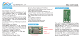
DS_DNM04SIP10_07162008D
2
TECHNICAL SPECIFICATIONS
(T
A
= 25°C, airflow rate = 300 LFM, V
in
= 2.8Vdc and 5.5Vdc, nominal Vout unless otherwise noted.)
PARAMETER NOTES and CONDITIONS DNM04S0A0R10
Min. Typ. Max. Units
ABSOLUTE MAXIMUM RATINGS
Input Voltage (Continuous) 0 5.8 Vdc
Tracking Voltage Vin,max Vdc
Operating Temperature Refer to Figure 45 for measuring point -40 125 °C
Storage Temperature -55 125 °C
INPUT CHARACTERISTICS
Operating Input Voltage
Vout ≦ Vin –0.5
2.8 5.5 V
Input Under-Voltage Lockout
Turn-On Voltage Threshold 2.2 V
Turn-Off Voltage Threshold 2.0 V
Maximum Input Current Vin=2.8V to 5.5V, Io=Io,max 10 A
No-Load Input Current 70 mA
Off Converter Input Current 5
mA
Inrush Transient Vin=2.8V to 5.5V, Io=Io,min to Io,max 0.1 A
2
S
Recommended Input Fuse 15 A
OUTPUT CHARACTERISTICS
Output Voltage Set Point
Vin=5V, Io=100% Io, max, Tc=25℃
-2.0 Vo,set +2.0
% Vo,set
Output Voltage Adjustable Range 0.7525 3.63 V
Output Voltage Regulation
Over Line Vin=2.8V to 5.5V 0.3 % Vo,set
Over Load Io=Io,min to Io,max 0.4 % Vo,set
Over Temperature Tc=-40℃ to 100℃ 0.8 % Vo,set
Total Output Voltage Range Over sample load, line and temperature -3.0 +3.0 % Vo,set
Output Voltage Ripple and Noise 5Hz to 20MHz bandwidth
Peak-to-Peak Full Load, 1µF ceramic, 10µF tantalum 25 50 mV
RMS Full Load, 1µF ceramic, 10µF tantalum 8
15
mV
Output Current Range 0 10 A
Output Voltage Over-shoot at Start-up Vout=3.3V 1 % Vo,set
Output DC Current-Limit Inception 220 % Io
Output Short-Circuit Current (Hiccup Mode) Io,s/c 3.5 Adc
DYNAMIC CHARACTERISTICS
Dynamic Load Response 10µF Tan & 1µF Ceramic load cap, 2.5A/µs
Positive Step Change in Output Current 50% Io, max to 100% Io, max 200 mV
Negative Step Change in Output Current 100% Io, max to 50% Io, max 200 mV
Settling Time to 10% of Peak Deviation 25 µs
Turn-On Transient Io=Io.max
Start-Up Time, From On/Off Control Vin=Vin,min, Vo=10% of Vo,set 4 ms
Start-Up Time, From Input Vo=10% of Vo,set 4
ms
Output Voltage Rise Time Time for Vo to rise from 10% to 90% of Vo,set 4 8 ms
Maximum Output Startup Capacitive Load
Full load; ESR ≧1mΩ
1000 µF
Full load; ESR ≧10mΩ
5000 µF
EFFICIENCY
Vo=3.3V
Vi=5V, 100% Load 96.0 %
Vo=2.5V Vi=5V, 100% Load 94.2 %
Vo=1.8V Vi=5V, 100% Load 92.4 %
Vo=1.5V Vi=5V, 100% Load 91.4 %
Vo=1.2V Vi=5V, 100% Load 90.0 %
Vo=0.75V Vi=5V, 100% Load 86.3 %
FEATURE CHARACTERISTICS
Switching Frequency 300 kHz
ON/OFF Control, (Negative logic)
Logic Low Voltage Module On, Von/off -0.2 0.3 V
Logic High Voltage Module Off, Von/off 1.5 Vin,max V
Logic Low Current Module On, Ion/off 10 µA
Logic High Current Module Off, Ion/off 0.2 1 mA
ON/OFF Control, (Positive Logic)
Logic High Voltage Module On, Von/off Vin,max V
Logic Low Voltage Module Off, Von/off -0.2 0.3 V
Logic Low Current Module On, Ion/off 0.2 1 mA
Logic High Current Module Off, Ion/off 10 µA
Tracking Slew Rate Capability 0.1 2 V/msec
Tracking Delay Time Delay from Vin.min to application of tracking voltage 10 ms
Tracking Accuracy Power-up 2V/mS 100 200 mV
Power-down 1V/mS 200 400 mV
Remote Sense Range 0.1 V
GENERAL SPECIFICATIONS
MTBF Io=80% of Io, max; Ta=25°C 21.91 M hours
Weight 10 grams
Over-Temperature Shutdown Refer to Figure 45 for measuring point 130 °C