Tandy PC-6 is a pocket scientific computer. It is a powerful tool that can be used to perform a variety of mathematical and scientific calculations. The PC-6 is also a programmable computer, which means that you can write your own programs to perform specific tasks.
The PC-6 has a number of features that make it ideal for students, engineers, and other professionals who need to perform complex calculations. These features include:
- A large, easy-to-read display
- A full set of mathematical and scientific functions
- The ability to store and recall programs
- A built-in clock and calendar
The PC-6 is also very easy to use. The keyboard is well-organized and the menus are clear and concise. The PC-6 also comes with a comprehensive user manual that will help you get started.


-
 1
1
-
 2
2
-
 3
3
-
 4
4
-
 5
5
-
 6
6
-
 7
7
-
 8
8
-
 9
9
-
 10
10
-
 11
11
-
 12
12
-
 13
13
-
 14
14
-
 15
15
-
 16
16
-
 17
17
-
 18
18
-
 19
19
-
 20
20
-
 21
21
-
 22
22
-
 23
23
-
 24
24
-
 25
25
-
 26
26
-
 27
27


Tandy PC-6 is a pocket scientific computer. It is a powerful tool that can be used to perform a variety of mathematical and scientific calculations. The PC-6 is also a programmable computer, which means that you can write your own programs to perform specific tasks.
The PC-6 has a number of features that make it ideal for students, engineers, and other professionals who need to perform complex calculations. These features include:
- A large, easy-to-read display
- A full set of mathematical and scientific functions
- The ability to store and recall programs
- A built-in clock and calendar
The PC-6 is also very easy to use. The keyboard is well-organized and the menus are clear and concise. The PC-6 also comes with a comprehensive user manual that will help you get started.
Ask a question and I''ll find the answer in the document
Finding information in a document is now easier with AI
Related papers
Other documents
-
Realistic LAB-2100 Owner's manual
-
Radio Shack 26-3651 User manual
-
OJ Electronics AHC-3000 PC-Tool Operating instructions
-
-
-
Genius 31300711109 Datasheet
-
-
-
Work-pro CS 310 T User manual
-
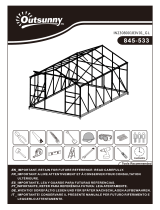 Outsunny 845-533V01 Assembly Instructions
