Texas Instruments AN-370 Techniques for Designing with CODEC/Filter COMBO Circuits Application Note
- Category
- Musical Equipment
- Type
- Application Note

AN-370 Techniques for Designing with CODEC/Filter COMBO Circuits
Literature Number: SNLA136

TL/Z/5734
Techniques for Designing with CODEC/Filter COMBO Circuits AN-370
National Semiconductor
Application Brief 370
Chris Stacey
Jim Wieser
Gary Rothrock
December 1991
Techniques for Designing
with CODEC/Filter
COMBO
É
Circuits
PCM CODEC/Filter COMBO devices are complex analog
and digital sub-systems on a single chip. They contain, for
example, an A/D and a D/A converter, each with 13 bit (for
u-law) resolution at low signal levels on the bottom chord of
the companding characteristic. The TP3050/60 family of
microCmos COMBOs are, however, capable of providing
extremely high performance even in the unfriendly electrical
environment of a multi-channel subscriber line card so long
as the printed circuit board is carefully designed as an inte-
gral part of the system. Indeed, this family can achieve per-
formance superior to that of other 1 or 2 chip CODEC/Filter
circuits due to two key factors; superior Power Supply Re-
jection Ratio, particularly at high frequencies, and the fact
that the critical connection between the transmit filter and
the encoder is carefully shielded inside the device. Never-
theless, the following guidelines should be adhered to in
order to maintain this high performance in any switching or
transmission system.
GROUND AND POWER SUPPLY LAYOUT
1. Different techniques are necessary for the layout of ana-
log circuits on the card (COMBO, SLIC and any external
gain sections) and the digital control and switching cir-
cuits. Use the GNDA pin of each COMBO device as the
Ground Reference Point (GRP) for each channel. All AN-
ALOG ground connections for each channel should con-
nect as close as possible to the reference point. This
includes:
a. The analog ground from the 4-wire side of the SLIC
circuit.
b. The ground for the transmit op amp connection.
c. The ground side of the 0.1 mF decoupling capacitors
for the
a
5V and
b
5V COMBO power supplies.
d. The analog ground for any external gain or loss adjust-
ment stage.
2. Ground return currents from logic circuits, relays and oth-
er audio channels must not flow into or out from the chan-
nel GRPs to avoid generating noise voltages. Therefore a
separate ground return should be run from each channel
GRP to a common point close to the ground pin on the
card connector, commonly called the MECCA. Thus there
is a STAR formation from the MECCA to each channel
GRP. It is NOT recommended to run separate analog and
digital ground returns to the shelf power supply. Relays
and other circuits operating from the station battery
should, however, have a separate return bus to the bat-
tery ground.
3. Decouple the
a
5V and
b
5V power supplies to the MEC-
CA close to the card connector. A minimum of 10 mF
should be used for each supply, and a capacitor type with
a low Effective Series Resistance should be selected. Be-
ware of the effects of the inrush current charging these
capacitors as the card is plugged into a ‘‘hot’’ socket.
This current flowing through the wire and trace induc-
tance can cause voltage spikes which easily exceed the
absolute maximum ratings of various devices on the card
and may even damage the connector contacts. The trace
length from the connector to the capacitors should be
kept short, and excessive values of decoupling capacitor
avoided.
4. The
a
5V and
b
5V supply busses to the COMBO circuits
should be routed adjacent to a ground bus to help ensure
that any r.f. noise pick-up is common mode. Each supply
must be decoupled by 0.1mF capacitors with short traces
to the GRP of each COMBO. Ceramic capacitors are best
for good high frequency decoupling.
5. The
a
5V bus for the switching and control logic circuits
should be a separate connection from the decoupled
point close to the card connector. It should not share any
common path with the
a
5V connection to the COMBO
circuits. Each logic circuit should be decoupled with a
0.01 mF ceramic capacitor from
a
5V to ground close to
the device.
6. The ground connections for the logic circuits and low volt-
age relays may use a ground bus or, better still, a ground
grid system to maintain good noise margins on digital sig-
nals. This logic ground should connect directly to the card
MECCA such that logic ground currents do not share
common paths with any channel GRP returns.
7. TTL and LSTTL logic families draw considerably different
supply currents when their outputs are in the high and low
logic states, causing large switching currents to flow
through the busses and decoupling capacitors. In con-
trast, CMOS logic circuits only draw significant currents
during state transitions, and these currents are substan-
tially balanced. A CMOS logic system therefore gener-
ates far less electrical noise than a similar TTL System.
The use of the 74HC CMOS logic family is highly recom-
mended for line card design. It helps to preserve high
performance transmission in the analog circuits and of-
fers better noise margins than TTL in the presence of
transient voltages induced by relays and ringing signals.
Always use
a
5V decoupling capacitors on each logic de-
vice when using ‘‘HC’’ CMOS logic.
COMBO
É
is a registered trademark of National Semiconductor Corporation.
C
1995 National Semiconductor Corporation RRD-B30M115/Printed in U. S. A.

NOISE CONSIDERATIONS
1. Logic signals should be routed well away from the analog
circuits and their power supply connections wherever
possible to minimize high frequency noise being capaci-
tively coupled into the channel and aliased down into the
audio passband by the sampling action of the filters and
encoder.
2. All signals and circuits capable of inducing large emf’s
into the audio signals should be located around the edge
of the card wherever possible. This includes:
a. Relay drive and output signals
b. Ringing distribution
c. The 2-wire side of the SLIC circuits.
d.
b
48V battery
e. d.c. to d.c. converters
3. Ground planes may be used to shield audio signals from
noise sources such as clock and data signals and the
high voltages listed above. A ground plane is only effec-
tive, however, if it carries NO NOISE-INDUCING CUR-
RENTS itself. A single point connection from the ground
plane to a quiet return is the best way to assure this.
4. The transmit op amp connections become a potential
noise source particularly if a high gain is required. The
feedback resistor value should not exceed 50K ohms,
and the bodies of the feedback and input resistors should
be close to the op amp input to minimize capacitive noise
pick-up.
5. In asynchronous applications (typically transmission sys-
tems) the best idle channel noise and signal/distortion
performance will be achieved if the transmit and receive
filters are clocked synchronously. Thus the MCLK
R
/PDN
input on the TP3050/60 COMBO devices should either
be connected to MCLK
X
or controlled solely by logic sig-
nals as a PDN input only (the COMBO will automatically
use MCLK
X
internally). Note that MCLK
R
does not need
to be synchronized to BCLK
R
and FS
R
.
CIRCUIT PROTECTION
CMOS CODEC/Filter COMBOs are capable of providing ex-
tremely reliable and stable long-term performance provided
a few simple precautions are followed:
1. Normal CMOS handling techniques should be used to
prevent build-up of static charge on the device. These
include the use of conductive carriers, and grounding per-
sonnel while handling devices.
2. Ensure that ground is always connected to each device
before any other supplies or signals. An extended ground
pin should be used on line card connectors.
3. Buffer all digital input and output signals between COM-
BO circuits and the line card backplane. This both pro-
tects the COMBO circuits from backplane transients and
preserves good logic signal transition times and noise
margins.
4. CMOS inputs, outputs and supply connections must be
protected against even momentary transitions outside the
supply voltages. Schottky diodes should be fitted on each
card between
a
5V and GND, and between GND and
b
5V to clamp transient power supply reversals during
power-up. Type 1N5820 is a good choice. If series supply
filters are used on a per COMBO basis, each COMBO
should have Schottky diodes across its supply pins. In
this case smaller diodes, such as 1N5817, can be used.
5. If the COMBO circuit is connected to a transformer-type
of SLIC circuit additional protection is required against
line transients. An input resistor of 5K ohms or more is
adequate to protect the transmit op amp inputs, VF
X
I
a
and VF
X
I
b
. If this is not possible, silicon diodes or a pair
of back-to-back 3.9V zener diodes (depending on the re-
quired dynamic range) should be connected between the
vulnerable input and GND.
6. A pair of back-to-back 3.9V zener diodes may also be
necessary to protect the receive power amplifier out-
put(s). Select a zener type with a sharp ‘‘knee’’ on the V-I
characteristic, and low leakage current at voltages below
the knee to avoid impairing the gain-tracking of the re-
ceive channel at high signal levels.
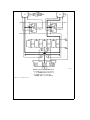
Figure 1
illustrates an idealized circuit card layout embody-
ing many of the above techniques. While space constraints
may limit the application of some of these techniques, the
closer they can be followed, the better the system perform-
ance will be.
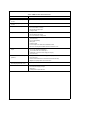
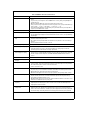
APPENDIX I. COMBO TROUBLESHOOTING GUIDE
Table I lists a number of troubles sometimes experienced
with COMBO devices and the potential causes of these
troubles. For each cause, Table II identifies appropriate so-
lutions.
2

TL/Z/5734– 1
FIGURE 1. Suggested COMBO PCB Layout
1. Use ‘STAR’ Connection For Each Channel
To The ‘CHANNEL GRP’ At GNDA (Pin 2)
2. Use ‘STAR’ Connections From Each
‘CHANNEL GRP’ To The PCB ‘MECCA’
Note: GRP
e
Ground Reference Point.
3

APPENDIX I. COMBO TROUBLESHOOTING GUIDE (Continued)
Table I. COMBO Troubles and Potential Causes
Trouble Potential Cause
#
No output at DX and VFRO
#
Device Powered Down
#
Tx AND Rx frequency response
#
Incorrect MCLK Frequency
incorrect
#
Only Rx frequency response
#
Incorrect Frame Sync Pulse Frequency
incorrect
#
High distortion at Dx output
#
Overdriving Input (VFXI)
#
Incorrect DC Bias on Tx Amp
#
Overloading Tx Amp Output
#
Timing Problem
#
High distortion at VFRO output
#
Timing Problem
#
Overloading Rx Amp Output
#
Incorrect Frame Sync Timing Mode
#
Idle Noise and/or S/D out of spec
#
Inadequate or Ineffective Power Supply Decoupling
#
Poor Grounding
#
Use of LSB Signalling
#
Noisy SLIC
#
Timing Problem
#
Tones in Output. See Next Item in TROUBLE Column
#
Error in Converting Absolute Measurements to Relative Levels
#
Low level tones or whistles in
#
Use of Asynchronous Clocks
output
#
Use of Unlocked Switching Supplies
#
Use of Jittered Clocks or Frame Syncs
#
Inadequate or Ineffective Power Supply Decoupling
#
Poor Grounding
#
Intrachannel Crosstalk out of spec
#
Inadequate or Ineffective Power Supply Decoupling
(4W Ckts)
#
Poor Grounding
#
Common Ground Return from Tx and Rx Line Interface Circuitry
#
Magnetic Coupling between Line Transformers
#
Device Gets Warm, Hot, Draws
#
Latch-up
Abnormally High Current or Dies
#
Other Causes of Trouble
#
Damaged Device
#
Incorrect Power Supply Voltages
#
Wiring Error
#
Testing Board on Extender Card
4

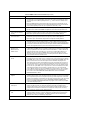
APPENDIX I. COMBO TROUBLESHOOTING GUIDE (Continued)
Table II. COMBO Trouble Causes and Solutions
Causes Solutions
#
Timing Problem
#
Verify with oscilloscope that all timing relationships at the COMBO pins meet data sheet
specs.
#
Loop device by connecting Dx to Dr. If COMBO works correctly, timing incompatibility with
system may exist.
#
MCLKx and BCLKx MUST be synchronous (derived from same clock).
#
Verify on all device logic inputs that noise and/or ringing does not go beyond allowable logic
levelsÐLOW
eb
0.3V to
a
0.6V, HIGH
ea
2.2V to V
CC
a
0.3V.
#
Verify BCLKR and MCLKR are not left floating. They should be driven by a low impedance
logic level, or hardwired if not clocked.
#
Damaged Device
#
Replace with known good device
#
Overdriving Input (VFXI)
#
The maximum signal at the Tx amplifier output pin (GSx) should never exceed
g
2.8V Peak.
The Tx amplifier input signal plus offset should therefore never exceed
g
2.8 Vpk divided by
amplifier gain.
#
Incorrect DC Bias on Tx
#
VFxI
a
MUST have a ground reference of 100k or less, preferably equal to the DC
Amp resistance seen looking out of VFxI
b
.
#
AC coupling of the input signal will be needed if there is any DC bias or offset exceeding a
few mV.
#
DC offset at GSx should not exceed
g
200 mV.
#
Overloading Tx Amp Output
#
Tx amplifier external load at GSx must be 10 kX or greater.
#
Overloading Rx Amp Output
#
Minimum load impedance is 600X
#
If load DC resistance is low (i.e., transformer winding), AC coupling may be needed to
prevent large DC current flow due to Rx Amp output offset.
#
Inadequate/Ineffective
#
0.1 mF ceramic disc decoupling capacitors (good high frequency characteristics) should be
Power Supply Decoupling placed from V
CC
to GND and V
BB
to GND as close as possible to the device pins. Cap lead
and trace lengths must be kept short. See GROUND AND POWER SUPPLY LAYOUT
section.
#
Poor Grounding
#
See GROUND AND POWER SUPPLY LAYOUT section.
#
Incorrect Power Supply
#
V
CC
should be
a
4.75 to
a
5.25V, V
BB
should be
b
4.75 to
b
5.25V.
Voltages
#
Wiring Error
#
Inspect ALL device pins with oscilloscope for presence of correct signals and absence of
incorrect signals. Inspection should be done directly on the device pins to ensure problems
due to bad solder joints or socket connections are found.
#
Device reversed in socket.
#
Device powered down
#
MCLKR/PDN pin must be connected to logic LOW or have clock signal applied for device to
be powered up. If connected HIGH or allowed to float HIGH, device will be powered down.
#
Missing frame sync pulses will cause device to power down.
#
MCLKx must be applied to the device for proper operation of the power up/down circuitry.
#
Incorrect MCLK frequency
#
The MCLKX and MCLKR applied frequency must be 2.048, 1.544 or 1.536 MHz. Other
frequencies will cause an error in Tx and Rx switched capacitor filter response directly
proportional to the MCLK frequency error.
#
BCLKR/CLKSEL pin must be connected as shown in datasheet Table I to select the correct
divide ratio for the MCLK frequency being used.
#
Incorrect Frame Sync Pulse
#
The Frame Sync frequency must be 8 kHz. The Rx filter has correction for (sin x)/x roll-off
frequency imparted by the decoder response. This correction is not accurate for FSR frequencies/
sampling rates other than 8 kHz.
#
Incorrect Frame Sync
#
The device assumes short frame sync timing at power on initialization. The Tx frame sync pin
Timing Mode (FSx) is monitored to determine if long frame timing is being used. If long frame timing is
used for the receive side and no Tx frame sync pulse is applied, the device will operate with
short frame timing, misreading the data and causing high level distortion (noise) at VFRO.
5

APPENDIX I. COMBO TROUBLESHOOTING GUIDE (Continued)
Table II. COMBO Trouble Causes and Solutions (Continued)
Causes Solutions
#
Use of LSB Signalling
#
Least Significant Bit Signalling, commonly used in T-1 channel banks, impacts noise and
S/D performance. In these applications, TP3052/53 are preferred over TP3054/64, as the
decoder interprets the LSB in signalling frames as ‘‘(/2’’ in these devices to minimize noise
and S/D.
#
Bellcore LSSGR (TR-TSY-000064, Class 5 Switch spec) bases S/D requirements on full
8-bit transmission. Measurements are done with LSB signalling turned off. If measurements
are done with signalling on, then the spec requirement is reduced by 1.1 dB.
#
Noisy SLIC
#
Use of a noisy semiconductor SLIC with the COMBO will impact performance, particularly if
high gain is also needed in the COMBO Tx Amplifier because the SLIC output level is low.
#
Common Ground Return
#
Common ground paths for Tx and Rx circuitry may have enough impedance to cause
from Tx/Rx Line Interface problems, especially in high load current circuits. Components such as line transformers
Circuitry MUST have separate ground return lines all the way back to the COMBO GND pin.
#
Magnetic Coupling between
#
Stray magnetic flux provides coupling between Rx and Tx transformers. This coupling can be
Line Transformers minimized by spacing the transformers as far apart as possible. Rotating adjacent
transformers by 90
§
will sometimes help as will use of magnetic shielding material.
#
Latch-up
#
Latch-up occurs due to violation of Absolute Maximum Ratings when signal voltages
instantaneously exceed power supply voltages, or supply voltage polarity reversals have
occurred. These may occur when power is applied to the system or a board is plugged into a
hot system, as well as other ways. See items 2 through 6 under the CIRCUIT PROTECTION
section of this Application Note for protection measures which must be used.
#
Error in Converting
#
Measurements of signal and noise levels at the device VFxI and VFrO pins in absolute units
Absolute Level of dBm, dBrnC and dBmp must be converted to relative levels for comparison to many data
Measurements to sheet spec parameters. Since the 0 dBm0 level at VFxI and VFrO is
a
4 dBm, 4 dB must be
Relative Levels subtracted from absolute level readings to convert these to relative dBm0, dBrnC0, and
dBm0p levels. This is true only for COMBO I devices and for measurements only at the
device pins. Other devices and points in the circuit will in general have different conversion
factors between absolute and relative levels.
#
Use of Asynchronous
#
The term ‘‘asynchronous clocks’’, as used here, refers to two logic signals which are derived
Clocks from different unlocked oscillator sources. If asynchronous clocks are used on the card with
the COMBO device, new ‘‘beat’’ frequencies will be generated within the COMBO due to the
highly non-linear nature of the switched capacitor filter and CODEC sampling functions.
These beat frequencies will be sum and difference frequencies between the asynchronous
clocks and their harmonics, some of which may fall within the speech band. In general, use
of asynchronous clocks should be avoided if at all possible. mC clocks, for example, should
be locked to the system PCM clocks. If asynchronous clocks are unavoidable, as in a PCM
channel bank application where Tx and Rx clocks and frame syncs come from different
sources, MCLKr should be synchronous with MCLKx for best performance. Also, grounding,
power supply decoupling and PCB layout is critical in applications involving asynchronous
clocks. See sections entitled GROUND AND POWER SUPPY LAYOUT and NOISE
CONSIDERATIONS for details.
#
Use of Unlocked Switching
#
Free running switching regulators, converters, etc. can cause problems similar to those
Supplies caused by asynchronous clocks. All switching supplies should be locked to the system PCM
clocks to prevent asynchronous noise spikes on power, ground and signal lines. If unlocked
supplies are unavoidable, extra attention must be paid to keeping grounds, power, and signal
lines free of the switching noise. See sections entitled GROUND AND POWER SUPPY
LAYOUT and NOISE CONSIDERATIONS. Switching supplies can be locked to any multiple
of the 8 kHz sampling frequency.
#
Use of Jittered Clocks or
#
Clocks are sometimes locked or recovered using digital PLLs, which impart jitter to the pulse
Frame Syncs stream. This will be passed on to the analog samples. If the peak to peak jitter is large
enough and the frequency lies in the speech band, it may be audible. The jitter frequency is
usually related to the difference between the incoming and local frequencies. An analog
phase locked loop should be used to eliminate the jitter.
#
Testing PCB on Extender
#
Use of an extender card sometimes causes problems during testing. Propagation delays,
Card capacitive loading, reflections, overshoot, ringing and crosstalk are all increased and may
cause timing, noise, or other problems. The extender should be removed temporarily to
determine if it is causing or contributing to the problem.
6

7

AN-370 Techniques for Designing with CODEC/Filter COMBO Circuits
LIFE SUPPORT POLICY
NATIONAL’S PRODUCTS ARE NOT AUTHORIZED FOR USE AS CRITICAL COMPONENTS IN LIFE SUPPORT
DEVICES OR SYSTEMS WITHOUT THE EXPRESS WRITTEN APPROVAL OF THE PRESIDENT OF NATIONAL
SEMICONDUCTOR CORPORATION. As used herein:
1. Life support devices or systems are devices or 2. A critical component is any component of a life
systems which, (a) are intended for surgical implant support device or system whose failure to perform can
into the body, or (b) support or sustain life, and whose be reasonably expected to cause the failure of the life
failure to perform, when properly used in accordance support device or system, or to affect its safety or
with instructions for use provided in the labeling, can effectiveness.
be reasonably expected to result in a significant injury
to the user.
National Semiconductor National Semiconductor National Semiconductor National Semiconductor
Corporation Europe Hong Kong Ltd. Japan Ltd.
1111 West Bardin Road Fax: (
a
49) 0-180-530 85 86 13th Floor, Straight Block, Tel: 81-043-299-2309
Arlington, TX 76017 Email: cnjwge
@
tevm2.nsc.com Ocean Centre, 5 Canton Rd. Fax: 81-043-299-2408
Tel: 1(800) 272-9959 Deutsch Tel: (
a
49) 0-180-530 85 85 Tsimshatsui, Kowloon
Fax: 1(800) 737-7018 English Tel: (
a
49) 0-180-532 78 32 Hong Kong
Fran3ais Tel: (
a
49) 0-180-532 93 58 Tel: (852) 2737-1600
Italiano Tel: (
a
49) 0-180-534 16 80 Fax: (852) 2736-9960
National does not assume any responsibility for use of any circuitry described, no circuit patent licenses are implied and National reserves the right at any time without notice to change said circuitry and specifications.

IMPORTANT NOTICE
Texas Instruments Incorporated and its subsidiaries (TI) reserve the right to make corrections, modifications, enhancements, improvements,
and other changes to its products and services at any time and to discontinue any product or service without notice. Customers should
obtain the latest relevant information before placing orders and should verify that such information is current and complete. All products are
sold subject to TI’s terms and conditions of sale supplied at the time of order acknowledgment.
TI warrants performance of its hardware products to the specifications applicable at the time of sale in accordance with TI’s standard
warranty. Testing and other quality control techniques are used to the extent TI deems necessary to support this warranty. Except where
mandated by government requirements, testing of all parameters of each product is not necessarily performed.
TI assumes no liability for applications assistance or customer product design. Customers are responsible for their products and
applications using TI components. To minimize the risks associated with customer products and applications, customers should provide
adequate design and operating safeguards.
TI does not warrant or represent that any license, either express or implied, is granted under any TI patent right, copyright, mask work right,
or other TI intellectual property right relating to any combination, machine, or process in which TI products or services are used. Information
published by TI regarding third-party products or services does not constitute a license from TI to use such products or services or a
warranty or endorsement thereof. Use of such information may require a license from a third party under the patents or other intellectual
property of the third party, or a license from TI under the patents or other intellectual property of TI.
Reproduction of TI information in TI data books or data sheets is permissible only if reproduction is without alteration and is accompanied
by all associated warranties, conditions, limitations, and notices. Reproduction of this information with alteration is an unfair and deceptive
business practice. TI is not responsible or liable for such altered documentation. Information of third parties may be subject to additional
restrictions.
Resale of TI products or services with statements different from or beyond the parameters stated by TI for that product or service voids all
express and any implied warranties for the associated TI product or service and is an unfair and deceptive business practice. TI is not
responsible or liable for any such statements.
TI products are not authorized for use in safety-critical applications (such as life support) where a failure of the TI product would reasonably
be expected to cause severe personal injury or death, unless officers of the parties have executed an agreement specifically governing
such use. Buyers represent that they have all necessary expertise in the safety and regulatory ramifications of their applications, and
acknowledge and agree that they are solely responsible for all legal, regulatory and safety-related requirements concerning their products
and any use of TI products in such safety-critical applications, notwithstanding any applications-related information or support that may be
provided by TI. Further, Buyers must fully indemnify TI and its representatives against any damages arising out of the use of TI products in
such safety-critical applications.
TI products are neither designed nor intended for use in military/aerospace applications or environments unless the TI products are
specifically designated by TI as military-grade or "enhanced plastic." Only products designated by TI as military-grade meet military
specifications. Buyers acknowledge and agree that any such use of TI products which TI has not designated as military-grade is solely at
the Buyer's risk, and that they are solely responsible for compliance with all legal and regulatory requirements in connection with such use.
TI products are neither designed nor intended for use in automotive applications or environments unless the specific TI products are
designated by TI as compliant with ISO/TS 16949 requirements. Buyers acknowledge and agree that, if they use any non-designated
products in automotive applications, TI will not be responsible for any failure to meet such requirements.
Following are URLs where you can obtain information on other Texas Instruments products and application solutions:
Products Applications
Audio www.ti.com/audio Communications and Telecom www.ti.com/communications
Amplifiers amplifier.ti.com Computers and Peripherals www.ti.com/computers
Data Converters dataconverter.ti.com Consumer Electronics www.ti.com/consumer-apps
DLP® Products www.dlp.com Energy and Lighting www.ti.com/energy
DSP dsp.ti.com Industrial www.ti.com/industrial
Clocks and Timers www.ti.com/clocks Medical www.ti.com/medical
Interface interface.ti.com Security www.ti.com/security
Logic logic.ti.com Space, Avionics and Defense www.ti.com/space-avionics-defense
Power Mgmt power.ti.com Transportation and Automotive www.ti.com/automotive
Microcontrollers microcontroller.ti.com Video and Imaging www.ti.com/video
RFID www.ti-rfid.com
OMAP Mobile Processors www.ti.com/omap
Wireless Connectivity www.ti.com/wirelessconnectivity
TI E2E Community Home Page e2e.ti.com
Mailing Address: Texas Instruments, Post Office Box 655303, Dallas, Texas 75265
Copyright © 2011, Texas Instruments Incorporated
-
 1
1
-
 2
2
-
 3
3
-
 4
4
-
 5
5
-
 6
6
-
 7
7
-
 8
8
-
 9
9
-
 10
10


Texas Instruments AN-370 Techniques for Designing with CODEC/Filter COMBO Circuits Application Note
- Category
- Musical Equipment
- Type
- Application Note
Ask a question and I''ll find the answer in the document
Finding information in a document is now easier with AI
Related papers
-
Texas Instruments LMH730121 Evaluation Board User guide
-
-
-
-
-
-
-
-
-
