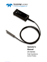
Tektronix TDP3500 Technical Reference

Type
Technical Reference

Tektronix TDP3500 is a high-performance differential probe designed to accurately measure and analyze high-speed signals in electronic circuits. It offers exceptional signal integrity, wide bandwidth, and low noise, making it ideal for debugging and characterizing high-speed digital designs. With its differential inputs, the TDP3500 can reject common-mode noise and capture true differential signals with precision.

Tektronix TDP3500 is a high-performance differential probe designed to accurately measure and analyze high-speed signals in electronic circuits. It offers exceptional signal integrity, wide bandwidth, and low noise, making it ideal for debugging and characterizing high-speed digital designs. With its differential inputs, the TDP3500 can reject common-mode noise and capture true differential signals with precision.

TDP3500
3.5 GHz Differential Probe
ZZZ
Technical Reference
xx
Revision A
www.tektronix.com
071-2297-00
Copyright © Tektronix. All rights reserved. Licensed software products are owned by Tektronix or its subsidiaries or suppliers, and are
protected by na
tional copyright laws and international treaty provisions.
Tektronix prod
ucts are covered by U.S. and foreign patents, issued and pending. Information in this publication s upersedes that in all
previously published material. Specications and price change privileges reserved.
TEKTRONIX and TEK are registered trademarks of Tektronix, Inc.
Contacting Tektronix
Tektronix, Inc.
14200 SW Karl B raun Drive
P.O. Box 500
Beaverton, OR 97077
USA
For product information, sales, service, and technical support:
In North America, call 1-800-833-9200.
Worldwide, visit www.tektronix.com to nd contacts in your area.
Warranty 2
Tektronix warrants that this product will be free from defects in materials and workmanship for a period of one (1) year from the date of
shipment. If any such product proves defective during this warranty period, Tektronix, at its option, either will repair the defective
product without charge for parts and labor, or will provide a replacement in exchange for the defective product. Parts, m odules and
replacement products used by Tektronix for warranty work may be new or reconditioned to like new performance. All replaced
parts, modules and products become the property of Tektronix.
In order to obtain service under this warranty, Customer must notify Tektronix of the defect before the expiration of the warranty period
and make suitable arrangements for the performance of service. Customer shall be responsible for packaging and shipping the
defective product to the service center designated by Tektronix, with shipping charges prepaid. Tektronix shall pay for the return of the
product to Customer if the shipment is to a location w ithin the country in which the Tektronix service center is located. Customer shall
be responsible for paying all shipping charges, duties, taxes, and any other charges for products returned to any other locations.
This warranty shall not apply to any defect, failure or damage caused by improper use or improper or inadequate maintenance and
care. Tektronix shall not be obligated to furnish service under this warranty a ) to repair damage resulting from attempts by personnel
other than Tektronix representatives to install, repair or service the product; b) to repair damage resulting from improper use or
connection to incompatible equipment; c) to repair any damage or malfunction caused by the use of non-Tektronix supplies; or
d) to service a product that has been modied or integrated with other products when the effect of such modication or integration
increases the time or difculty of servicing the product.
THIS WARRANTY IS GIVEN BY TE KTR ONIX WITH RES PEC T TO THE PROD UC T IN LIEU OF ANY OTH ER WARRANTIES,
EXPRESS OR IMPLIED. TEKTRONIX AND ITS VENDO RS DISCLAIM ANY IMPLIED WARRANTIES OF MERCHANTABILITY OR
FITNESS FOR A PARTICULAR PURPOSE. TEK TRONIX’ RES PON SIBILITY TO REPAIR O R REPLACE DEFECTIVE PRODUCTS
IS THE SOLE AND EXCLUSIVE REMEDY PROVIDED TO T HE CUSTOMER FOR BREACH OF THIS WARRANTY. TEKTRONIX
AND ITS VENDORS W ILL NOT BE LIABLE FOR ANY INDIRECT, SPECIAL, INCIDENTAL, OR CONSEQUENTIAL DAMAGES
IRRESPECTIVE O F WHETHER TEKTRONIX OR THE VENDOR HAS ADVANCE NOTICE OF THE POSSIBILITY O F SUCH
DAMAGES.
Table of Content
s
Table of Contents
General Safety Summary .............................. ... . .. . . . . .. . .................... ... . .. . . . . .. . .................... ... . .. . . . . . .. iii
Preface................................................................................................................................. v
Specications .......................................................................................................................... 1
Warranted Characteristics............................................................................................................. 2
Typical Charac
teristics ................................................................................................................ 3
Nominal Characteristics ............................................................................................................... 6
Probe Tip Adapter Specications ..................................................................................................... 7
Performance Ve
rication ............................................................................................................. 11
Required Equipment ............... ... . . . . .. . ................. . .. . . . . .................... . . . . .................... . . . . ... ........ 11
Special Adapters ................................................................................................................ 12
Preparation ....... ... ... ... ... ... ... ... ... ... ... ...... . .. ... ... ... ... ... ... ... ... ... ... ... ... ... ... ...... . .. ... ... ... ... ... ... ... 14
DC Attenuation Accuracy .... ... ......... ...... ......... ...... ...... ......... ...... ......... ...... ......... ...... ......... ...... 15
Differential Signal Range ............. ... . . . . .. . ................. . .. . . . . .................... . . . . .................... . . . . ... ..... 17
Rise Time........................................................................................................................18
Maintenance .......................................................................................................................... 23
Inspection and Cleaning .. ... . .. . . . . .. . .................... ... . .. . . . . .. . .................... ... . .. . . . . .. . .................... ... 23
Replacement Par
ts.............................................................................................................. 23
Preparation for Shipment .......... . .. . . . . ... ................. ... . . . . .. . .................... . . . . .. . .................... . . . . ... .. 23
TDP3500 Technical Reference i
Table of Content
s
ii TDP3500 Technical Reference
General Safety S
ummary
General Safet
y Summary
Review the following safety precautions to avoid injury and prevent damage to this product or any products connected to it.
To avoid potential hazards, use this product only as specied.
Only qualied personnel should perform service procedures.
While using this product, you may need to access other parts of a l arger system. Read the safety s ections of the other
component manuals for warnings and cautions related to operating the system.
To Avoid Fire or Personal Injury
Connect and Disconnect Properly. Do not connect or disconnect probes or test leads while they are connected
to a voltage s
ource.
Ground the Pro
duct.
This product is indirectly grounded through the grounding conductor of the mainframe power cord.
To avoid electric shock, the grounding conductor must be connected to earth ground. Before making connections to the input
or output terminals of the product, ensure that the product is properly grounded.
Observe All Terminal Ratings. To avoid re or shock hazard, observe all ratings and markings on the product. Consult
the product m
anual for further ratings information before making connections to the product.
Connect the p
robe reference lead to earth ground only.
Do not apply a
potential to any terminal, including the common terminal, that exceeds the maximum rating of that terminal.
Do Not Operat
e Without Covers.
Do not operate this product with covers or panels removed.
Do Not Operat
e With Suspected Failures.
If you suspect that there is damage to this product, have it inspected by
qualied service personnel.
Avoid Exposed Circuitry. Do not touch exposed connections and components when power is present.
Do Not Operate in Wet/Damp Conditions.
Do Not Operate in an Explosive Atmosphere.
Keep Product Surfaces Clean and Dry.
TDP3500 Technical Reference iii
General Safety S
ummary
TermsinthisManual
These terms may appear in this manual:
WARNING. Warning statements identify conditions or practices that could result in injury or loss of life.
CAUTION. Caution statements identify conditions or practices that could result in damage to this product or other property.
Symbols and Terms on the Product
These terms may appear on the product:
DANGER indicates an injury hazard immediately accessible as you read the marking.
WARNING indicates an injury hazard not immediately accessible as you r ead the marking.
CAUTION indicates a hazard to property including the product.
The following symbol(s) may appear on the product:
iv TDP3500 Technical Reference
Preface
Preface
This is the Technical Reference Manual for the TDP3500 differential probe. This manual provides specications and
performance verication procedures for the probe.
TDP3500 Technical Reference v
Preface
vi TDP3500 Technical Reference
Specications
Specication
s
The specications in Tables 1 through 4 apply to a TDP3500 differential probe installed on a Tektronix DPO 7000 oscilloscope.
When the probe is used with another oscilloscope, the oscilloscope must have an input impedance of 50 and a bandwidth
of 1 G Hz. The probe must have a warm-up period of at least 20 m inutes and be in an environment that does not exceed the
limits described. (See Table 1.) The probe calibration and Autozero routines should be run on the host instrument before
verifying the warranted probe specications. Specications for the TDP3500 differential probe fall into three categories:
warranted, typical, and nominal characteristics.
TDP3500 Technical Reference 1
Warranted Chara
cteristics
Warranted Cha
racteristics
Warranted characteristics describe guaranteed performance wit hin tolerance limits or certain type-tested requirements. (See
Table 1.) Warranted characteristics that have checks in the Performance Verication section are marked with the
symbol.
Table 1: Warranted electrical characteristics
Specication TDP3500
Differential signal range (DC coupled)
±2.0 V
(DC + peak AC)
Common-mode signal range (DC coupled)
+5 V to –4 V
(DC + peak AC)
Maximum non destructive input voltage
between signal and common of the same
channel
±15 V
(DC + peak AC)
DC attenuation accuracy
±2% of input
Bandwidth (probe only) DC to 3.5 GHz
Rise time, probe only
(10–90%, + 20 °C to + 30 °C)
140 ps
Common-mode rejection ratio
>60 dB at DC
>55dBat1MHz
>45dBat30MH
z
>25dBat1GHz
Temperature
Operating: 0 to +40 °C (32 °F to +104 °F)
Nonoperating: –40 to +71 °C (–40 °F to –159 °F)
1
Humidity
Operating: 0-90% RH, tested at + 30 to +40 °C
Nonoperatin
g: 0-90% RH, tested at +30 to +60 °C
1
See warning that follows.
WARNING. To avoid a burn hazard at high ambient temperatures, do not touch the probe with bare hands at nonoperating
temperatures above +50 °C .
2 TDP3500 Technical Reference
Typical Charact
eristics
Typical Chara
cteristics
Typical characteristics describe typical but not guaranteed performance.
Table 2: Typical electrical characteristics
Differential input resistance, DC coupled 100 k
Common mode input resistance 50 k
Differential input capacitance
<0.3 pF at 10 MHz
Common-mode input capacitance
<0.45 pF per side at 100 MHz
Offset accuracy
±10 mV
Differential offset range
±1 V
Common mode rejection ratio (See Figure 3 on page 4.)
System noise
Referred to probe input
<35 nVHz @ 100 MHz
Input impedance
(See Figure 4 on page 5.)
Propagation delay
5.4 ns ±2 ns from probe tip to output
Figure 1: Typical bandwidth
TDP3500 Technical Reference 3
Typical C haract
eristics
Figure 2: Typical rise time
Figure 3: Typical Common-Mode Rejection Ratio
4 TDP3500 Technical Reference
Typical Charact
eristics
Figure 4: Ty
pical input impedance versus frequency
Table 3: Typical mechanical characteristics
Dimensions, input connection
0.63 mm (0.025 in) square pin sockets on 2.54 mm
(0.100 in) centers
Dimensions, control box
117mm×41mm×29mm(4.6in×1.6in×1.15in)
Dimensions, probe head
86 mm × 11 mm × 8.9 mm (3.4 in × 0.45 in × 0.35 in)
Dimensions, output cable
1.22 m (48 in)
Unit weight (probe only) 144.5 g (5.1 oz)
Figure 5: P robe dimensions
TDP3500 Technical Reference 5
Nominal Charact
eristics
Nominal Chara
cteristics
Nominal characteristics describe guaranteed traits, but the traits do not have tolerance limits.
Table 4: Nominal electrical characteristics
Input conguration Differential (two inputs, + and - ), with case ground
Output coupling DC coupling
Voltage range
+/–2 V
Termination
Terminate output into 50
6 TDP3500 Technical Reference
Probe Tip Adapte
r Specications
Probe Tip A dap
ter Specications
This section describes the characteristics of the adapters that are included in your accessory kit. The adapters are listed
in order of performance, beginning with the fastest. You will get the best probe performance by c onnecting the probe
directly to square pins on your circuit. However, as test points are not always as convenient, these adapters m ake taking
measurements easier while maintaining the best signal delity.
NOTE. A ll adapter specications are typical unless otherwise indicated.
Variable Spacing Adapter
Tektronix pa
rt number: 016-1885-xx
Bandwidth: <
3.5 GHz
10/90 Rise ti
me: <110 ps
This adapter
has adjustable pins that can span from 0.020 to 0.180 inch apart.
TDP3500 Technical Reference 7
Probe Tip Adapte
rSpecications
Square Pin Adapter
Tektronix part number: 016-1884-xx
Bandwidth: <3.3 GHz
10/90 Rise time: <110 ps
Use this adapter to provide easy access to square-pin test points that you frequently check, or to other probe accessories.
8 TDP3500 Technical Reference
Probe Tip Adapte
r Specications
Solder-in Adapter Kit
Tektronix part number: 020-2505-xx Solder-in Adapter Kit
(Includes two adapters, Tektronix part number 016-1926-xx, and a R esistor/Wire Kit, Tektronix part number 020-2506-xx)
You can reorder either kit. The Resistor/Wire Kit includes ten each resistors (10 and 20 bonded to 0.020 in wire), and
ten lengths of 0 .020 in solder wire. The kit also includes ten each resistors (10 and 20 bonded to 0.008 in wire), and
ten lengths of 0.008 in solder wire.
Bandwidth: <4.3 GHz (Solder wire), <3.8 GHz (10 resistor), <3.7 GH z (20 resistor)
10/90 Rise time: <124 ps (Solder wire), <131 ps (10 resistor), <140 ps (20 resistor)
Use this adapter on test points that you frequently check that do not have square pins or other convenient connections.
Solder the wire or resistor leads that come with the kit to your test points.
CAUTION. To prevent short circuits, solder and dress the adapter leads carefully, and make sure that the leads do not touch
other conductors when the adapter is not connected to the probe.
To prevent damaging this adapter, do not connect it to 0.025” square pins. Instead, use the square-pin adapter included
in the probe accessory kit.
TDP3500 Technical Reference 9
Probe Tip Adapte
rSpecications
Y-Lead Adapte
r
Tektronix part number: 196-3434-xx
Usable Bandwidth: <100 MHz
Calculated rise time: 1.4 ns
Use this adapter for DC and low-frequency m easurements. The socket ends plug onto s quare pins, component leads, and
the MicroCKT Test Tip adapters included with the probe.
MicroCKT T
est Tips
Tektronix part number: 206-0569-xx
Usable Bandwidth: <100 MHz
Calculated rise time: 3.5 ns
Use the MicroCKT Test Tips with the Y-lead adapters. Due to the length of these adapters, they are only r ecommended for
DC and low-frequency measurements.
10 TDP3500 Technical Reference
  • Page 1 1
  • Page 2 2
  • Page 3 3
  • Page 4 4
  • Page 5 5
  • Page 6 6
  • Page 7 7
  • Page 8 8
  • Page 9 9
  • Page 10 10
  • Page 11 11
  • Page 12 12
  • Page 13 13
  • Page 14 14
  • Page 15 15
  • Page 16 16
  • Page 17 17
  • Page 18 18
  • Page 19 19
  • Page 20 20
  • Page 21 21
  • Page 22 22
  • Page 23 23
  • Page 24 24
  • Page 25 25
  • Page 26 26
  • Page 27 27
  • Page 28 28
  • Page 29 29
  • Page 30 30
  • Page 31 31
  • Page 32 32
  • Page 33 33

Tektronix TDP3500 Technical Reference

Type
Technical Reference

Tektronix TDP3500 is a high-performance differential probe designed to accurately measure and analyze high-speed signals in electronic circuits. It offers exceptional signal integrity, wide bandwidth, and low noise, making it ideal for debugging and characterizing high-speed digital designs. With its differential inputs, the TDP3500 can reject common-mode noise and capture true differential signals with precision.

Ask a question and I''ll find the answer in the document

Finding information in a document is now easier with AI