
Application Brief
SPRA465
Digital Signal Processing Solutions June 1999
Designing the TMS320C548/9 DSP
Development Board
Art Chen Digital Signal Processing Solutions
John Wong
Abstract
This application brief describes the design of the Texas Instruments (TI™)TMS320C548/9
development board (DVB) from both the hardware and software approach. The DVB is a simple
stand-alone application board used to evaluate the performance and characteristics of the
TMS320LC548-80, TMS320LC549-80, and TMS320VC549-80 digital signal processor (DSP)
hardware and software.
The TMS320C548/9 DVB contains two boards connected by two box-style connectors:
TMS320C548/9 DSP board
Analog interface circuit (AIC) board
The DVB contains the TMS320LC548 or TMS320VC549 DSP and provides full-speed verification
of TMS320C54x codes. The DVB transmits and receives the audio signals via the AIC and
operational amplifier (OP Amp, OPA) port. The DVB transmits and receives the PSTN signals via
the AIC and data access arrangement (DAA) port. The DVB connects with the XDS-510 (JTAG—
Joint Testing Action Group, IEEE1149.1 Standard) and uses the TMS320C54x ('C54x) emulation
software as a debugging tool.
This application brief discusses the technologies behind the power system, clock, AIC/OPA,
AIC/DAA, and DSP. We focus on the memory configuration and code development for direct
communication between on-chip synchronized serial port and serial devices AIC, aspecially on
the telephony.
The authors extend their deep appreciation to Kevin Chang, Max Chyou, and Ted Lee from the
ASP-WCBU application team; Ryan Hsiao from MSLP; Mandy Tsai from the Taiwan FAE team;
and the members of the DSP champion team for their invaluable help in this project.

Application Brief
SPRA465
Designing the TMS320C548/9 DSP Development Board 2
Contents
Introduction......................................................................................................................................................3
TMS320LC548, LC549, and VC549 DSPs ......................................................................................................4
JTAG (XDS-510)..............................................................................................................................................7
Power System..................................................................................................................................................8
External Program Memory...............................................................................................................................9
TLC320AD50 Analog Interface Circuit...........................................................................................................13
TLC2274 Operational Amplifier......................................................................................................................15
Public Service Telephone Network Interface .................................................................................................16
Layout Issues and Connector Definition.........................................................................................................17
Appendix A. TMS320C548/9 Development Board Schematics.....................................................................19
Appendix B. Bill of Materials .........................................................................................................................32
References.....................................................................................................................................................34
Figures
Figure 1. TMS320C548/9 DVB Block Diagram .............................................................................................3
Figure 2. TMS320LC548 DSP PGE Package Top View...............................................................................5
Figure 3. TMS320LC549 and VC549 DSP PGE Package Top View ............................................................6
Figure 4. JTAG Cable Header and Signals...................................................................................................7
Figure 5. Power and Ground System............................................................................................................8
Figure 6. Configuration of the External Memory............................................................................................9
Figure 7. DSP External Memory Read Timing............................................................................................11
Figure 8. SRAM Read Timing.....................................................................................................................11
Figure 9. DSP External Memory Write Timing ............................................................................................12
Figure 10. SRAM Write Timing .....................................................................................................................12
Figure 11. TLC320AD50 Functional Block Diagram......................................................................................13
Figure 12. AIC Connect With DSP by Synchronous Serial Port....................................................................14
Figure 13. Differential Input...........................................................................................................................15
Figure 14. Single Ending Output...................................................................................................................16
Figure 15. PSTN Interface ............................................................................................................................17
Figure 16. TMS320C548/9 Development Board...........................................................................................19
Figure 17. TMS320C548/9 DSP Board.........................................................................................................19
Figure 18. TMS320C548/9 DSP and Clock...................................................................................................20
Figure 19. TMS320C548/9 Development Board JTAG Connector................................................................21
Figure 20. TMS320C548/9 Development Board Power System...................................................................22
Figure 21. TMS320C548/9 Development Board 128K Words (Type 1) Memory System..............................23
Figure 22. TMS320C548/9 Development Board 256K Words (Type 2) Memory System..............................24
Figure 23. TMS320C548/9 Development Board I/O Connectors on DSP Board ..........................................25
Figure 24. Analog Interface Circuit Board.....................................................................................................26
Figure 25. TMS320C548/9 Development Board I/O Connectors on AIC Board............................................27
Figure 26. Audio Interface.............................................................................................................................28
Figure 27. PSTN Control Interface................................................................................................................29
Figure 28. PSTN Interface ............................................................................................................................30
Figure 29. TMS320C548/9 Development Board Placement .........................................................................31

Application Brief
SPRA465
Designing the TMS320C548/9 DSP Development Board 3
Introduction
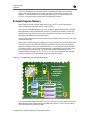
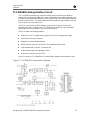
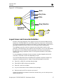
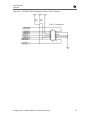
The TMS320C548/9 DVB enhances the ability to create your own project by
implementing software codes, building connection boards, and expanding your system as
desired. Figure 1 shows the DVB block diagram, which includes the following
components:
TMS320LC548PGE-80, TMS320LC549PGE-80, or TMS320VC549PGE-80 DSP
128K words or 256K words SRAM program memory space
JTAG (Joint Testing Action Group, XDS-510) port
Power supply for 5 V, 3.3 V, 2.5 V
12.288-MHz oscillator for both the DSP and the analog interface
TLC320AD50C AIC and TLC2274 operational amplifier for the audio interface port
TLC320AD50C AIC and Ericsson PBL-38581 DAA for the PSTN interface port
Figure 1. TMS320C548/9 DVB Block Diagram
Power Supply
5, 3.3 & 2.5 VDC
Power Supply
Power Supply
5, 3.3 & 2.5 VDC
5, 3.3 & 2.5 VDC
J
J
T
T
A
A
G
G
TMS320
TMS320
TMS320
C548/9
C548/9
C548/9
AIC
and
OPA
AIC
AIC
and
and
OPA
OPA
S
R
A
M
S
S
R
R
A
A
M
M
Extension Connector
Extension Connector
Extension Connector
PSTNPSTN
PSTN
The TMS320C54x generation of the TI TMS320 DSP is fabricated using static CMOS
integrated circuit technology. The combination of advanced modified Harvard architecture
with one program bus and three data memory buses, additional on-chip peripherals, on-
chip data memory, and a highly specialized instruction set is the basis for the operational
flexibility and speed of this device.

Application Brief
SPRA465
Designing the TMS320C548/9 DSP Development Board 4
TMS320LC548, LC549, and VC549 DSPs
The TMS320LC548, TMS320LC549, and TMS320VC549 DSPs are packaged in a 144-
pin PGE TQFP (selected) and 144-pin GGU BGA and include the following features:
Low-power enhanced-architecture device (LEAD) core CPU
Advanced Multibus architecture With three separate 16-bit data memory buses and
one program memory bus
40-bit arithmetic logic unit (ALU), including a 40-bit barrel shifter and two Independent
40-bit accumulators
Compare, select, and store unit (CSSU) for the add/compare selection of the Viterbi
operator
Two address generators with eight auxiliary registers and two auxiliary register
arithmetic units (ARAUs)
8192K x 16-bit program memory, 64K x 16- bit data memory, and 64K x 16-bit I/O
memory space
On-chip 16-bit timer
Single-instruction repeat and block repeat operations for program code
Block-memory-move Instructions for better program and data management
Wait states software programmable to each space
Phase-locked loop (PLL), software programmable
One time-division multiplexed (TDM) serial port
Two buffered serial ports (BSPs)
XDS-510 (JTAG) port, fully supported
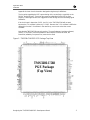
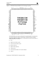
Figure 2 and Figure 3 show the top view of the 144-pin TMS320LC548, TMS320LC549,
and TMS320VC549 DSP PGE packages, which include the following pin groups:
Parallel data (D0~D15), address bus (A0~A22), and memory control signals
Used for data transfer between the DSP and external memory
Initialization, interrupts, and reset operation control pins
Provide direct control of the DSP
Synchronous serial port (BSP and TDM) signals
Communicates with the host or other devices having the same kind of the port
Multiprocessing signals
Cooperates with other DSPs
Oscillator, PLL, and timer signals
Power supply pins in TMS320VC549
CVDD and CVSS are provided for the CPU, and DVDD and DVSS are provided for
the peripheral.
JTAG signals
Defined in the IEEE1149.1 standard and accessed by the emulator

Application Brief
SPRA465
Designing the TMS320C548/9 DSP Development Board 5
Appendix A shows circuit schematics designed using these pin definitions.
The key point regarding the DSP system design is the control logic, especially on the
READY and HOLD pins. These two pins must be pulled high for the DSP to work
properly. Pulled-high resistors are suggested for the driving current and floating signal
avoidance.
If the clock input is lower than 2 VDC, the PLL in the TMS320LC549 will not work
because the 5-V oscillator is driven by 3.3 VDC. Because the 3.3-V oscillator is difficult to
distinguish from the 5-V oscillator in the retail shop, use care to select the correct
oscillator.
Note that the TMS320C549 can only use the C Source Debugger (emulator software)
revision 1.70 or later. If the EMU5xxWM for the multiple DSP must be used, the
Board.Dat (edited by Composer.Exe) must also be used.
Figure 2. TMS320LC548 DSP PGE Package Top View
TMS320LC548
TMS320LC548
PGE Package
PGE Package
(Top View)
(Top View)

Application Brief
SPRA465
Designing the TMS320C548/9 DSP Development Board 6
Figure 3. TMS320LC549 and VC549 DSP PGE Package Top View
TMS320LC549
TMS320LC549
TMS320VC549
TMS320VC549
PGE Package
PGE Package
(Top View)
(Top View)
The TMS320C54x is the most cost-effective DSP chip with high MIPS in the fixed-point
DSP family, especially in wireless communication. The device is built on the high-
performance LEAD core and integrates on-chip peripherals that make it well-suited for a
variety of applications, including:
GSM
Digital communication system
Personal communication system
Wireless local loop
Digital cordless telephony
Feature phones
Phone-like data modems for LCD phone displays
Caller ID

Application Brief
SPRA465
Designing the TMS320C548/9 DSP Development Board 7
DTMF
Voice mail
Centrex modems
The TMS320C54x DSP is designed so that manufacturers of high-volume applications
can reap the benefits of high-performance DSPs without paying the higher prices
historically associated with them. System code and hardware development for the LEAD
core is supported using JTAG scan-based emulation. The serial scan interface to the
core is bonded out of the device so that the XDS-510 system emulator can interface with
the DSP core. In this way, the system tested and verified using the TMS320C548/9 DVB
can be designed with or without a connection board (AIC board).
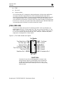
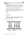
JTAG (XDS-510)
To perform emulation with the XDS-510 following the IEEE 1149.1 specification, the
target system must have a 14-pin header (two 7-pin rows, pin-to-pin spacing = 0.1", pin
size = 0.025 in
2
, pin length = 0.235") with connections shown in Figure 4. Seven pins on
the TMS320C54x DSP chip are used for the JTAG. These pins, as well as the power
supply pins, are mapped to the 14-pin header.
Figure 4. JTAG Cable Header and Signals
Test Mode Select
Test Mode Select
- TMS
- TMS
Test Data Input
Test Data Input
- TDI
- TDI
Presence Detect
Presence Detect
- PD
- PD
Test Data Output
Test Data Output
- TDO
- TDO
Test Clock Return
Test Clock Return
- TCK_RET
- TCK_RET
Test Clock
Test Clock
- TCK
- TCK
Emulation Pin 0
Emulation Pin 0
- EMU0
- EMU0
TRST -
TRST -
Test Reset
Test Reset
GND -
GND -
Ground
Ground
No Pin (Key)
No Pin (Key)
GND -
GND -
Ground
Ground
GND -
GND -
Ground
Ground
GND -
GND -
Ground
Ground
EMU1 -
EMU1 -
Emulation Pin 1
Emulation Pin 1
7
7
x
x
2 Header
2 Header
0.2
0.2
”
”
x
x
0.7
0.7
“
“
2
2
4
4
6
6
8
8
10
10
12
12
14
14
1
1
3
3
5
5
7
7
9
9
11
11
13
13
C
C
A
A
U
U
T
T
I
I
O
O
N
N
:
:
Cut the No Pin (pin 6) to avoid plugging the connector in the
wrong direction and thus connecting the Presence Detect pin
(5) with ground and the GND pin (10) with VCC (3.3 V). This
would connect the Presence Detect pin and VCC with possibly
serious results.

Application Brief
SPRA465
Designing the TMS320C548/9 DSP Development Board 8
Power System
The power system design of the TMS320C548/9 DVB is 5 VDC, 3.3 VDC, and 2.5 VDC.
The DVB includes more capacitors for noise bypass and an LED as a power indicator.
The DC-5V adapter with DJ005A 2.1 connector is used. The 5 VDC supports analog
devices such as the AIC and OP Amp. The 3.3 VDC supports most of the digital devices.
If the TMS320VC549 is used, the 2.5 VDC is required for the CPU core only.
The DVB design includes the TI TPS7150, TPS7133, and TPS71025 micropower low-
dropout (LDO) voltage regulators to satisfy power supply requirements.
The most important design consideration for the DVB power system is to use several
ferrite beads (a kind of core, 800 ohms/100 MHz = 1.27 H) between each VCC and
each ground to avoid noise and EMI (electromagnetic interference) issues (see Figure 5).
Because the resistance of the inductor in the frequency domain is
Z(f) = j2 fL
where
j
= the image value
f
= the frequency value
L
= the inductor value
thus, the high frequency of the noise generated from the digital ground cannot interfere
with the analog ground. Analog devices, such as the AIC and OPA, will work more stable
than before. In addition, this approach avoids noise and EMI problems because the
analog devices are used always as the front-end components.
Figure 5. Power and Ground System
A
A
AVCC
AVCC
5VCC
5VCC
C
C
C
C
C
C
C
C
R
R
LED
LED
FB
FB
Controlled by Frequency
Controlled by Frequency
Frequency =
Frequency =
0
0
Frequency =
Frequency =
=
=
FB
FB
5
5

Application Brief
SPRA465
Designing the TMS320C548/9 DSP Development Board 9
The other consideration for noise prevention is shielding and cutting. Some ground
portions are spread equally on the board, and these ground shields separate noise
radiation. To avoid excessive noise passing by GND or VCC, the area (such as the
PSTN) is cut from the power system and connected with a thread.
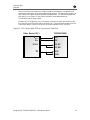
External Program Memory
When selecting SRAM, memory depth (how many K size?) is more important than
memory width (how many bits, nibbles, bytes, words?).
The reason is that additional glue logic (such as the OR gate) should be used, although
extra gate delay will be generated. Because the very high-speed SRAM is hard to find
and expensive, and memory access time is important for the DSP system design, any
other logic gate will delay system performance.
The other point is that because most memory control signal is active low, the control logic
must be inverse logic.
Many kinds of internal memory configurations can be used with the TMS320C548/9 DVB.
The 32K DARAM in the TMS320LC548 and TMS320VC549 can be used as program
memory or data memory and is controlled by OVLY. An important fact should be noted.
The internal memory can be used as data memory or data/program memory but cannot
be used as program memory only. This means that external data memory can be
selected only from 8000h to FFFFh, if OVLY = 1. Thus, the best method uses internal
memory as data memory and external memory as program memory.
Figure 6. Configuration of the External Memory
TMS320
TMS320
TMS320
C548/9
C548/9
C548/9
Memory Configuration :
Memory Configuration :
1. Controlled by
1. Controlled by
Program Space
Program Space
2. Controlled by
2. Controlled by
Data Space
Data Space
1.
2.
Data Bus
Data Bus
128K8
SRAM
128
128
K8
K8
SRAM
SRAM
128K8
SRAM
128
128
K8
K8
SRAM
SRAM
Upper Byte
Upper Byte
Lower Byte
Lower Byte
256K4 SRAM
256
256
K4 SRAM
K4 SRAM
256K4 SRAM
256
256
K4 SRAM
K4 SRAM
256K4 SRAM
256
256
K4 SRAM
K4 SRAM
256K4 SRAM
256
256
K4 SRAM
K4 SRAM
1
1
st
st
Nibble
Nibble
2
2
nd
nd
Nibble
Nibble
3
3
rd
rd
Nibble
Nibble
4
4
th
th
Nibble
Nibble
Type 2
Type 2
Address Bus
Address Bus
Type 1
Type 1
The TMS320C548/9 DVB 128K-word (Type 1) or 256K-word (Type 2) external memory is
determined while the components are mounted (see Figure 6). The memory should be
very high-speed asynchronous SRAMs.

Application Brief
SPRA465
Designing the TMS320C548/9 DSP Development Board 10
Because the more than 66 MIPS calculation capability is applied in the TMS320C548/9
DVB, the program SRAM access time must be around 10 ns. Table 1 summarizes the
relationship between the MIPS and the access time of the program SRAM. The larger
value is for reference only because the required high-speed SRAM is expensive and
difficult to find. On the DVB, the 8-ns SRAM is working properly with the TMS320LC548-
80 in 80 MIPS.
Table 1. Relationship Between MIPS and SRAM Access Time
DSP Calculation Capability
(MIPS)
SRAM Access Time
‘LC54x-80 (ns)
SRAM Access Time
‘VC54x-100 (ns)
63 8.4 < t < 15.4 9.9 < t < 15.9
66 7.7 < t < 14.7 9.2 < t < 15.2
73 6.2 < t < 13.2 7.7 < t < 13.7
80 5 < t < 12 6.5 < t < 12.5
100 4 < t < 10
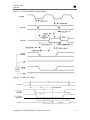
Figure 7 through Figure 10 show the memory read and write timing diagrams of the
external memory system. In these diagrams, the key elements are t
a(A)m
, t
su(D)R
,. and t
h(D)R
.
For example, if the TMS320LC548-80 is used and the speed is 80 MIPS, the access time
must be 12.5 – 7.5 = 5 ns. It is no guarantee, but, if the TI process is trustworthy, the
t
su(D)R
(setup time) and t
h(D)R
(hold time) can be taken as part of the access time.
Therefore, he access time might be extended to 12.5 – 7.5 + 5 + 2 = 12 ns (too
dangerous).
An OR gate controls the read and write on SRAM by MSTRB and R/W; at least 3.5 ns
absolutely required. If the DSP is reading, no transaction time is needed because R/W is
always high. Because the writing time is much longer than the reading time, the gate
delay of the OR gate must be acceptable.

Application Brief
SPRA465
Designing the TMS320C548/9 DSP Development Board 11
Figure 7. DSP External Memory Read Timing
Figure 8. SRAM Read Timing
=
=
Access Time
Access Time
=
=
PS or DS
PS or DS
=
=
Pulled Low
Pulled Low

Application Brief
SPRA465
Designing the TMS320C548/9 DSP Development Board 12
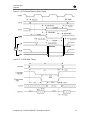
Figure 9. DSP External Memory Write Timing
RW
RW
OR
OR
3.5
3.5
nS
nS
min
min
3.5
3.5
nS
nS
min
min
Figure 10. SRAM Write Timing
=
=
RW
RW
=
=
PS or DS
PS or DS

Application Brief
SPRA465
Designing the TMS320C548/9 DSP Development Board 13
TLC320AD50 Analog Interface Circuit
The TLC320AD50 provides high-resolution analog signal conversion from digital-to-
analog (D/A) and analog-to-digital (A/D) using oversampling sigma-delta technology and
includes an interpolation filter before the D/A converter (DAC) and a decimation filter after
the A/D converter (ADC). The sigma-delta architecture produces high resolution A/D and
D/A conversion at a low system cost.
The AIC is connected to the DSP using the synchronous serial port. Because the
Master/Slave mode is supported in the TLC320AD50, the multi-line or the multi-signal
input/output can be executable in a synchronous serial port.
The AIC includes the following features:
Requires 3.3 VDC for digital power supply and 5 VDC for analog power supply
Synchronous serial port Interface
Requires one-order anti-aliasing filter
88-dB dynamic-range ADC and DAC in 2s-complement data format
Programmable ADC and DAC conversion rate
Programmable input and output gain control
Maximum conversion rate: 22.05 kHz
Figure 11 shows the TLC320AD50 AIC functional block diagram and package top view.
Figure 11. TLC320AD50 Functional Block Diagram

Application Brief
SPRA465
Designing the TMS320C548/9 DSP Development Board 14
Use the asynchronous serial port to send information controlling the configuration and
performance parameters by several available data registers. The data in the registers set
up the device for a given mode of operation and application. The anti-aliasing input low-
pass filter is a one-order R-C filter, which should be connected between the
TLC320AD50 and the input signals.
Because the TLC320AD50 is only a one-frame, synchronous signal, we should connect
the 'C54x/FSR and 'C54x/FSX with the 'AD50/FS pin. The transmit and receive clock are
of the same design. Figure 12 shows the connection between the AIC and DSP.
Figure 12. AIC Connect With DSP by Synchronous Serial Port
TMS320C548/9
TMS320C548/9
DR
DR
DX
DX
CLKX
CLKX
CLKR
CLKR
FSX
FSX
FSR
FSR
D
D
OUT
OUT
D
D
IN
IN
SCLK
SCLK
___
___
FS
FS
Other Device (AIC)
Other Device (AIC)

Application Brief
SPRA465
Designing the TMS320C548/9 DSP Development Board 15
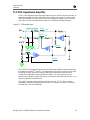
TLC2274 Operational Amplifier
The AIC uses differential input and single-ending output on the DVB and thus requires an
operational amplifier (OP Amp, OPA). Because the AIC uses a single 5-V power supply
on the analog portion, we should take care of the middle point voltage (V
MID
). Figure 13
and Figure 14 show the differential input with V
MID
and differential output designs.
Figure 13. Differential Input
AVCC
2
A
A
A
AVCC
AVCC
2
-
-
-
IN
IN+
IN-
AVCC
2
-
IN
AVCC
2
+ IN
Anti-Aliasing Filter
-
-
-
-
-
-
A
A
A
A
A
A
AVCC
2
The TLC2274 is an audio band quad rail-to-rail operational amplifier manufactured using
the advanced LinCMOS
TM
process. The advanced LinCMOS process uses a silicon-gate
technology to obtain input offset voltage stability with temperature and time that far
exceeds that obtainable using metal-gate technology. This technology also makes
possible input impedance levels that meet or exceed levels offered by top-gate JFET and
expensive dielectric-isolated devices.
The single 5-V power supply should be offered to this chip. The TLC2274 combines
outstanding output drive capability with low power consumption, excellent DC precision,
fast slew rates, and wide bandwidth.

Application Brief
SPRA465
Designing the TMS320C548/9 DSP Development Board 16
Figure 14. Single Ending Output
AVCC
AVCC
2
2
AVCC
OUT-
AVCC
AVCC
2
2
-
-
OUT-
OUT-
AVCC
AVCC
2
2
OUT
-
-
-
-
-
-
A
A
A
To enlarge the input and output signals, semi-variable resistors are used as input
resistors of the operational amplifiers. Unfortunately, because the DC signals are
enlarged along with the AC signals, the operational amplifiers are easily saturated. For
this reason, two capacitors are cascaded between the operational amplifiers and the I/O
connectors as the AC couplers. Only AC signals that are large enough can be received
and transmitted.
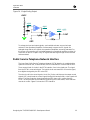
Public Service Telephone Network Interface
The Loop-Start Public Service Telephone Network (PSTN) interface is combined with a
hybrid circuit and an AIC, a latched buffer, and a 3-state buffer to connect with the DSP.
There are two kinds of circuits in the PSTN Interface. One is the signal part. The signal
from the PSTN is a two-wire signal. The hybrid circuit must transfer to a four-wire signal,
then digitize the signal by the AIC to the DSP.
The other circuit is the control signals. Hook, Dial_Pulse, and Mute are the output control
signals. DSP should send the control signals through the latched buffer, or the signals will
be lost. The Ring_Detection input signal tells the DSP that a call is coming from the
PSTN. The DSP should connect with this signal using the 3-state buffer, or the data bus
must be in conflict. Figure 15 shows the PSTN Interface.

Application Brief
SPRA465
Designing the TMS320C548/9 DSP Development Board 17
Figure 15. PSTN Interface
TMS320
TMS320
TMS320
C548/9
C548/9
C548/9
Hook
Hook
Dial_Pulse
Dial_Pulse
Mute
Mute
Ring_Detection
Ring_Detection
AIC
AIC
AIC
Synchronous
Synchronous
Serial Port
Serial Port
Hybrid
Hybrid
Hybrid
Latched
Latched
Buffer
Buffer
Tri
Tri
-State
-State
Buffer
Buffer
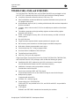
Layout Issues and Connector Definition
Because of the high frequencies of the signals running on the data and address buses
between the TMS320C548/9 DSP and SRAMs, these two components must be placed
as close and symmetrical as possible to each other. For the same reason, much noise is
generated around these buses, which is why a four-layer board is implemented.
The shielding by ground on both the component and solder side is used for noise
prevention. This technology is very useful for noise absorption, so the cross talk between
the signal lines can be reduced. But this technology must not be used everywhere.
Because high energy is produced in the PSTN, the ground should be cut to avoid the
noise source.
For easy debugging and testing, the test connectors are placed together with the I/O
connectors. These two connects are duplicated pin-to-pin.
The TMS320C548/9 DVB offers the flexibility DSP application engineers require in an
evaluation or development tool. A variety of component packages can be used:
Either DIP or SMD LED and ferrite-bead package
Either 0805 or 0603 resistors and capacitors
Either full- or half-size oscillator
Any one of three kinds of semi-variable resistor packages
Both phone jack and RCA connector can be used
Several connectors for the extension board are reserved; thus, you can make your own
design using the DVB.

Application Brief
SPRA465
Designing the TMS320C548/9 DSP Development Board 18
A basic rule in connector definition is that any VCC must not short with any GND in any
situation. This means that the system will not be shorted even if customers make a
mistake.
The second rule is to assign the power pins as much as possible to ensure system
stability.

Application Brief
SPRA465
Designing the TMS320C548/9 DSP Development Board 19
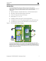
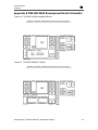
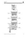
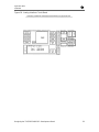
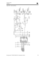
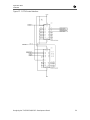
Appendix A. TMS320C548/9 Development Board Schematics
Figure 16. TMS320C548/9 Development Board
Figure 17. TMS320C548/9 DSP Board

Application Brief
SPRA465
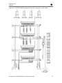
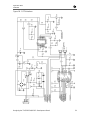
Designing the TMS320C548/9 DSP Development Board 20
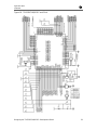
Figure 18. TMS320C548/9 DSP and Clock
Page is loading ...
Page is loading ...
Page is loading ...
Page is loading ...
Page is loading ...
Page is loading ...
Page is loading ...
Page is loading ...
Page is loading ...
Page is loading ...
Page is loading ...
Page is loading ...
Page is loading ...
Page is loading ...
Page is loading ...
Page is loading ...
-
 1
1
-
 2
2
-
 3
3
-
 4
4
-
 5
5
-
 6
6
-
 7
7
-
 8
8
-
 9
9
-
 10
10
-
 11
11
-
 12
12
-
 13
13
-
 14
14
-
 15
15
-
 16
16
-
 17
17
-
 18
18
-
 19
19
-
 20
20
-
 21
21
-
 22
22
-
 23
23
-
 24
24
-
 25
25
-
 26
26
-
 27
27
-
 28
28
-
 29
29
-
 30
30
-
 31
31
-
 32
32
-
 33
33
-
 34
34
-
 35
35
-
 36
36


Motorola SD7561-2 - C51 Communication System Cordless Phone Application Note
- Type
- Application Note
- This manual is also suitable for
Ask a question and I''ll find the answer in the document
Finding information in a document is now easier with AI
Related papers
Other documents
-
Texas Instruments TMS320C54x DSP CPU and Peripherals Reference Set Volume 1 (Rev. G) User guide
-
-
Cyrus CYRUS 8 User manual
-
-
Alcatel-Lucent AIC 2 User manual
-
-
-
-
AMX Interfacing the TLV320AIC12/13/14/15 Codec to the TMS320C5402? DSP Specification
-
Sony DVP-S300 Owner's manual