
FUJITSU SEMICONDUCTOR
CONTROLLER MANUAL
F
2
MC-8FX
8-BIT MICROCONTROLLER
PROGRAMMING MANUAL
CM26-00301-2E


FUJITSU LIMITED
F
2
MC-8FX
8-BIT MICROCONTROLLER
PROGRAMMING MANUAL


i
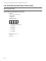
PREFACE
■ Purpose and Audience
The F
2
MC-8FX is original 8-bit one-chip microcontrollers that support application specific IC
(ASIC). It can be widely applied from household to industrial equipment starting with portable
equipment.
This manual is intended for engineers who actually develop products using the F
2
MC-8FX
microcontrollers, especially for programmers who prepare programs using the assembly
language for the F
2
MC-8FX series assembler. It describes various instructions for the F
2
MC-
8FX.
Note: F
2
MC is the abbreviation of FUJITSU Flexible Microcontroller.
■ Trademark
The company names and brand names herein are the trademarks or registered trademarks of
their respective owners.
■ Organization of This Manual
This manual consists of the following six chapters:
CHAPTER 1 OUTLINE AND CONFIGURATION EXAMPLE OF F
2
MC-8FX CPU
This chapter outlines the F
2
MC-8FX CPU and explains its configuration by example.
CHAPTER 2 MEMORY SPACE
This chapter explains the F
2
MC-8FX CPU memory space.
CHAPTER 3 REGISTERS
This chapter explains the F
2
MC-8FX dedicated registers and general-purpose registers.
CHAPTER 4 INTERRUPT PROCESSING
This chapter explains the functions and operation of F
2
MC-8FX interrupt processing.
CHAPTER 5 CPU SOFTWARE ARCHITECTURE
This chapter explains the instructions for the F
2
MC-8FX CPU.
CHAPTER 6 DETAILED RULES FOR EXECUTION INSTRUCTIONS
This chapter explains each execution instruction, used in the assembler, in reference format.
APPENDIX
The appendix contains instruction and bus operation lists and an instruction map.

ii
Copyright© 2004-2008 FUJITSU LIMITED All rights reserved.
• The contents of this document are subject to change without notice.
Customers are advised to consult with sales representatives before ordering.
• The information, such as descriptions of function and application circuit examples, in this document are presented solely for
the purpose of reference to show examples of operations and uses of FUJITSU semiconductor device; FUJITSU does not
warrant proper operation of the device with respect to use based on such information. When you develop equipment
incorporating the device based on such information, you must assume any responsibility arising out of such use of the
information. FUJITSU assumes no liability for any damages whatsoever arising out of the use of the information.
• Any information in this document, including descriptions of function and schematic diagrams, shall not be construed as license
of the use or exercise of any intellectual property right, such as patent right or copyright, or any other right of FUJITSU or any
third party or does FUJITSU warrant non-infringement of any third-party's intellectual property right or other right by using
such information. FUJITSU assumes no liability for any infringement of the intellectual property rights or other rights of third
parties which would result from the use of information contained herein.
• The products described in this document are designed, developed and manufactured as contemplated for general use, including
without limitation, ordinary industrial use, general office use, personal use, and household use, but are not designed, developed
and manufactured as contemplated (1) for use accompanying fatal risks or dangers that, unless extremely high safety is
secured, could have a serious effect to the public, and could lead directly to death, personal injury, severe physical damage or
other loss (i.e., nuclear reaction control in nuclear facility, aircraft flight control, air traffic control, mass transport control,
medical life support system, missile launch control in weapon system), or (2) for use requiring extremely high reliability (i.e.,
submersible repeater and artificial satellite).
Please note that FUJITSU will not be liable against you and/or any third party for any claims or damages arising in connection
with above-mentioned uses of the products.
• Any semiconductor devices have an inherent chance of failure. You must protect against injury, damage or loss from such
failures by incorporating safety design measures into your facility and equipment such as redundancy, fire protection, and
prevention of over-current levels and other abnormal operating conditions.
• Exportation/release of any products described in this document may require necessary procedures in accordance with the
regulations of the Foreign Exchange and Foreign Trade Control Law of Japan and/or US export control laws.
• The company names and brand names herein are the trademarks or registered trademarks of their respective owners.

iii
CONTENTS
CHAPTER 1 OUTLINE AND CONFIGURATION EXAMPLE OF F
2
MC-8FX CPU ........... 1
1.1 Outline of F
2
MC-8FX CPU .................................................................................................................. 2
1.2 Configuration Example of Device Using F
2
MC-8FX CPU .................................................................. 3
CHAPTER 2 MEMORY SPACE ........................................................................................ 5
2.1 CPU Memory Space ........................................................................................................................... 6
2.2 Memory Space and Addressing .......................................................................................................... 7
2.2.1 Data Area ...................................................................................................................................... 9
2.2.2 Program Area .............................................................................................................................. 11
2.2.3 Arrangement of 16-bit Data in Memory Space ............................................................................ 13
CHAPTER 3 REGISTERS ............................................................................................... 15
3.1 F
2
MC-8FX Registers ........................................................................................................................ 16
3.2 Program Counter (PC) and Stack Pointer (SP) ................................................................................ 17
3.3 Accumulator (A) and Temporary Accumulator (T) ............................................................................ 18
3.3.1 How To Use The Temporary Accumulator (T) ............................................................................. 20
3.3.2 Byte Data Transfer and Operation of Accumulator (A) and Temporary Accumulator (T) ............ 21
3.4 Program Status (PS) ......................................................................................................................... 23
3.5 Index Register (IX) and Extra Pointer (EP) ....................................................................................... 26
3.6 Register Banks ................................................................................................................................. 27
3.7 Direct Banks ..................................................................................................................................... 28
CHAPTER 4 INTERRUPT PROCESSING ...................................................................... 29
4.1 Outline of Interrupt Operation ........................................................................................................... 30
4.2 Interrupt Enable/Disable and Interrupt Priority Functions ................................................................. 32
4.3 Creating an Interrupt Processing Program ....................................................................................... 34
4.4 Multiple Interrupt ............................................................................................................................... 36
4.5 Reset Operation ................................................................................................................................ 37
CHAPTER 5 CPU SOFTWARE ARCHITECTURE ......................................................... 39
5.1 Types of Addressing Modes ............................................................................................................. 40
5.2 Special Instructions ........................................................................................................................... 43
CHAPTER 6 DETAILED RULES FOR EXECUTION INSTRUCTIONS .......................... 47
6.1 ADDC (ADD Byte Data of Accumulator and Temporary Accumulator with Carry to Accumulator)
48
6.2 ADDC (ADD Byte Data of Accumulator and Memory with Carry to Accumulator) ............................ 50
6.3 ADDCW (ADD Word Data of Accumulator and Temporary Accumulator with Carry to Accumulator)
52
6.4 AND (AND Byte Data of Accumulator and Temporary Accumulator to Accumulator) ...................... 54
6.5 AND (AND Byte Data of Accumulator and Memory to Accumulator) ............................................... 56
6.6 ANDW (AND Word Data of Accumulator and Temporary Accumulator to Accumulator) ................. 58

iv
6.7 BBC (Branch if Bit is Clear) .............................................................................................................. 60
6.8 BBS (Branch if Bit is Set) .................................................................................................................. 62
6.9 BC (Branch relative if C=1)/BLO (Branch if LOwer) ......................................................................... 64
6.10 BGE (Branch Great or Equal: relative if larger than or equal to Zero) .............................................. 66
6.11 BLT (Branch Less Than zero: relative if < Zero) ............................................................................... 68
6.12 BN (Branch relative if N = 1) ............................................................................................................. 70
6.13 BNZ (Branch relative if Z = 0)/BNE (Branch if Not Equal) ................................................................ 72
6.14 BNC (Branch relative if C = 0)/BHS (Branch if Higher or Same) ...................................................... 74
6.15 BP (Branch relative if N = 0: PLUS) .................................................................................................. 76
6.16 BZ (Branch relative if Z = 1)/BEQ (Branch if Equal) ......................................................................... 78
6.17 CALL (CALL subroutine) ................................................................................................................... 80
6.18 CALLV (CALL Vectored subroutine) ................................................................................................. 82
6.19 CLRB (Clear direct Memory Bit) ....................................................................................................... 84
6.20 CLRC (Clear Carry flag) ................................................................................................................... 86
6.21 CLRI (CLeaR Interrupt flag) .............................................................................................................. 88
6.22 CMP (CoMPare Byte Data of Accumulator and Temporary Accumulator) ....................................... 90
6.23 CMP (CoMPare Byte Data of Accumulator and Memory) ................................................................ 92
6.24 CMP (CoMPare Byte Data of Immediate Data and Memory) ........................................................... 94
6.25 CMPW (CoMPare Word Data of Accumulator and Temporary Accumulator) .................................. 96
6.26 DAA (Decimal Adjust for Addition) .................................................................................................... 98
6.27 DAS (Decimal Adjust for Subtraction) ............................................................................................. 100
6.28 DEC (DECrement Byte Data of General-purpose Register) ........................................................... 102
6.29 DECW (DECrement Word Data of Accumulator) ........................................................................... 104
6.30 DECW (DECrement Word Data of Extra Pointer) ........................................................................... 106
6.31 DECW (DECrement Word Data of Index Pointer) .......................................................................... 108
6.32 DECW (DECrement Word Data of Stack Pointer) .......................................................................... 110
6.33 DIVU (DIVide Unsigned) ................................................................................................................. 112
6.34 INC (INCrement Byte Data of General-purpose Register) .............................................................. 114
6.35 INCW (INCrement Word Data of Accumulator) .............................................................................. 116
6.36 INCW (INCrement Word Data of Extra Pointer) ............................................................................. 118
6.37 INCW (INCrement Word Data of Index Register) ........................................................................... 120
6.38 INCW (INCrement Word Data of Stack Pointer) ............................................................................. 122
6.39 JMP (JuMP to address pointed by Accumulator) ............................................................................ 124
6.40 JMP (JuMP to effective Address) ................................................................................................... 126
6.41 MOV (MOVE Byte Data from Temporary Accumulator to Address Pointed by Accumulator) ........ 128
6.42 MOV (MOVE Byte Data from Memory to Accumulator) .................................................................. 130
6.43 MOV (MOVE Immediate Byte Data to Memory) ............................................................................. 132
6.44 MOV (MOVE Byte Data from Accumulator to memory) .................................................................. 134
6.45 MOVW (MOVE Word Data from Temporary Accumulator to Address Pointed by Accumulator)
136
6.46 MOVW (MOVE Word Data from Memory to Accumulator) ............................................................. 138
6.47 MOVW (MOVE Word Data from Extra Pointer to Accumulator) ..................................................... 140
6.48 MOVW (MOVE Word Data from Index Register to Accumulator) ................................................... 142
6.49 MOVW (MOVE Word Data from Program Status Register to Accumulator) .................................. 144
6.50 MOVW (MOVE Word Data from Program Counter to Accumulator) .............................................. 146
6.51 MOVW (MOVE Word Data from Stack Pointer to Accumulator) .................................................... 148
6.52 MOVW (MOVE Word Data from Accumulator to Memory) ............................................................. 150
6.53 MOVW (MOVE Word Data from Accumulator to Extra Pointer) ..................................................... 152

v
6.54 MOVW (MOVE Immediate Word Data to Extra Pointer) ................................................................ 154
6.55 MOVW (MOVE Word Data from Accumulator to Index Register) ................................................... 156
6.56 MOVW (MOVE Immediate Word Data to Index Register) .............................................................. 158
6.57 MOVW (MOVE Word data from Accumulator to Program Status Register) ................................... 160
6.58 MOVW (MOVE Immediate Word Data to Stack Pointer) ................................................................ 162
6.59 MOVW (MOVE Word data from Accumulator to Stack Pointer) ..................................................... 164
6.60 MULU (MULtiply Unsigned) ............................................................................................................ 166
6.61 NOP (NoOPeration) ........................................................................................................................ 168
6.62 OR (OR Byte Data of Accumulator and Temporary Accumulator to Accumulator) ........................ 170
6.63 OR (OR Byte Data of Accumulator and Memory to Accumulator) .................................................. 172
6.64 ORW (OR Word Data of Accumulator and Temporary Accumulator to Accumulator) .................... 174
6.65 PUSHW (PUSH Word Data of Inherent Register to Stack Memory) .............................................. 176
6.66 POPW (POP Word Data of Intherent Register from Stack Memory) .............................................. 178
6.67 RET (RETurn from subroutine) ....................................................................................................... 180
6.68 RETI (RETurn from Interrupt) ......................................................................................................... 182
6.69 ROLC (Rotate Byte Data of Accumulator with Carry to Left) .......................................................... 184
6.70 RORC (Rotate Byte Data of Accumulator with Carry to Right) ....................................................... 186
6.71 SUBC (SUBtract Byte Data of Accumulator from Temporary Accumulator with Carry to Accumulator)
188
6.72 SUBC (SUBtract Byte Data of Memory from Accumulator with Carry to Accumulator) .................. 190
6.73 SUBCW (SUBtract Word Data of Accumulator from Temporary Accumulator with Carry to Accumulator)
192
6.74 SETB (Set Direct Memory Bit) ........................................................................................................ 194
6.75 SETC (SET Carry flag) ................................................................................................................... 196
6.76 SETI (SET Interrupt flag) ................................................................................................................ 198
6.77 SWAP (SWAP Byte Data Accumulator "H" and Accumulator "L") .................................................. 200
6.78 XCH (eXCHange Byte Data Accumulator "L" and Temporary Accumulator "L") ............................ 202
6.79 XCHW (eXCHange Word Data Accumulator and Extrapointer) ..................................................... 204
6.80 XCHW (eXCHange Word Data Accumulator and Index Register) ................................................. 206
6.81 XCHW (eXCHange Word Data Accumulator and Program Counter) ............................................. 208
6.82 XCHW (eXCHange Word Data Accumulator and Stack Pointer) ................................................... 210
6.83 XCHW (eXCHange Word Data Accumulator and Temporary Accumulator) .................................. 212
6.84 XOR (eXclusive OR Byte Data of Accumulator and Temporary Accumulator to Accumulator) ...... 214
6.85 XOR (eXclusive OR Byte Data of Accumulator and Memory to Accumulator) ............................... 216
6.86 XORW (eXclusive OR Word Data of Accumulator and Temporary Accumulator to Accmulator)
218
APPENDIX ......................................................................................................................... 221
APPENDIX A Instruction List ...................................................................................................................... 222
A.1 F
2
MC-8FX CPU Instruction Overview ............................................................................................ 223
A.2 Operation List ................................................................................................................................. 226
A.3 Flag Change Table ......................................................................................................................... 233
APPENDIX B Bus Operation List ............................................................................................................... 240
APPENDIX C Instruction Map .................................................................................................................... 251
INDEX................................................................................................................................... 253

vi

vii
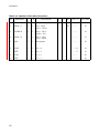
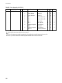
Main changes in this edition
The vertical lines marked in the left side of the page show the changes.
Page Changes (For details, refer to main body.)
11 2.2.2 Program Area
Table 2.2-2 CALLV Jump Address Table
( " FFC8
H
" → " FFC9
H
" )
53 Execution example : ADDCW A
( NZVC = "1010" → NZVC = "0000" )
147 Execution example : MOVW A, PC
( A = "F0 63" → A = "F0 62" )
( PC = "F0 63" → PC = "F0 62" )
176 6.65 PUSHW (PUSH Word Data of Inherent Register to Stack Memory)
( " Transfer the word value from the memory indicated by SP to dr. Then, subtract 2 fromthe value of SP. " →
" Subtract 2 from the value of SP. Then, transfer the word value from the memory indicated by SP to dr. " )
6.65 PUSHW (PUSH Word Data of Inherent Register to Stack Memory)
■ PUSHW (PUSH Word Data of Inherent Register to Stack Memory)
( "((SP)) <-- (dr) (Word transfer) " → " (SP) ← (SP) - 2 (Word subtraction) " )
( " (SP) <-- (SP) - 2 (Word subtraction) " → " ((SP)) ← (dr) (Word transfer) " )
226 A.2 Operation List
( "((iX)+off) <-- d8 " → " ((IX)+off) ← d8 " )
232 Table A.2-4 Operation List (for Other Instructions)
( "(SP) ← (SP)-2, ((SP)) ← (A)
(A) ← ((SP)),
(SP ) ← (SP)+2
(SP) ← (SP)-2,
((SP)) ← (IX)
(IX) ← ((SP)),
(SP) ← (SP)+2
No operation
(C) ← 0
(C) ← 1
(I) ← 0
(I) ← 1 " ) is added.

viii


2
CHAPTER 1 OUTLINE AND CONFIGURATION EXAMPLE OF F
2
MC-8FX CPU
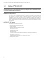
1.1 Outline of F
2
MC-8FX CPU
The F
2
MC-8FX CPU is a high-performance 8-bit CPU designed for the embedded control
of various industrial and OA equipment.
■ Outline of F
2
MC-8FX CPU
The F
2
MC-8FX CPU is a high-performance 8-bit CPU designed for the control of various industrial and
OA equipment. It is especially intended for applications requiring low voltages and low power
consumption. This 8-bit CPU can perform 16-bit data operations and transfer and is suitable for
applications requiring 16-bit control data. The F
2
MC-8FX CPU is upper compatibility CPU of the F
2
MC-
8L CPU, and the instruction cycle number is shortened, the division instruction is strengthened, and a direct
area is enhanced.
■ F
2
MC-8FX CPU Features
The F
2
MC-8FX CPU features are as follows:
• Minimum instruction execution time: 100 ns
• Memory: 64 Kbytes
• Instruction configuration suitable for controller
Data type: bit, byte, word
Addressing modes: 9 types
High code efficiency
16-bit data operation: Operations between accumulator (A) and temporary accumulator (T)
Bit instruction: set, reset, check
Multiplication/division instruction: 8 × 8 = 16 bits, 16/16 = 16 bits
• Interrupt priorities : 4 levels

3
CHAPTER 1 OUTLINE AND CONFIGURATION EXAMPLE OF F
2
MC-8FX CPU
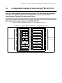
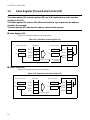
1.2 Configuration Example of Device Using F
2
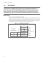
MC-8FX CPU
The CPU, ROM, RAM and various resources for each F
2
MC-8FX device are designed in
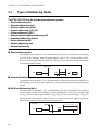
modules. The change in memory size and replacement of resources facilitate
manufacturing of products for various applications.
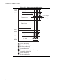
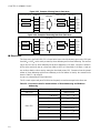
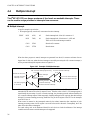
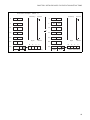
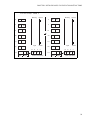
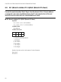
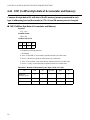
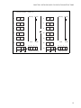
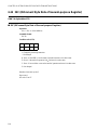
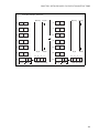
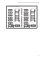
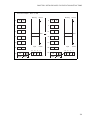
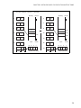
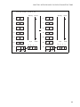
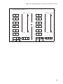
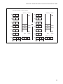
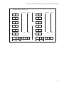
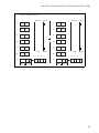
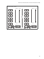
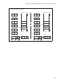
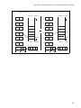
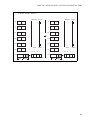
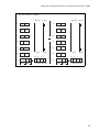
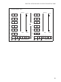
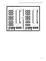
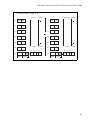
■ Configuration Example of Device Using F
2
MC-8FX CPU
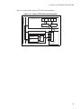
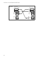
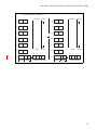
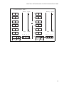
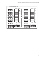
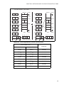
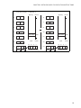
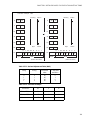
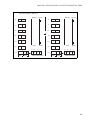
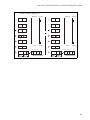
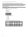
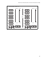
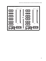
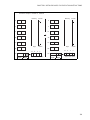
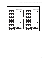
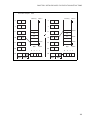
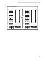
Figure 1.2-1 shows a configuration example of a device using the F
2
MC-8FX CPU.
Figure 1.2-1 Configuration Example of Device Using F
2
MC-8FX CPU
Timer/counter
A T
IX EP Serial port
PC SP
A/D converter
Common pins
RP CCR
PWM
ALU
RAM
ROM
Clock generator
Interrupt controller
External bus control section
Pins inherent to the product
Pins inherent
to the product
F
2
MC-8FX CPU
F
2
MC-8FX BUS
F
2
MC-8FX Device

4
CHAPTER 1 OUTLINE AND CONFIGURATION EXAMPLE OF F
2
MC-8FX CPU


6
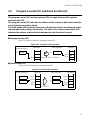
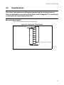
CHAPTER 2 MEMORY SPACE
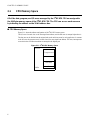
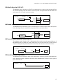
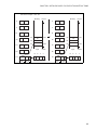
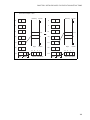
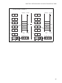
2.1 CPU Memory Space
All of the data, program, and I/O areas managed by the F
2
MC-8FX CPU are assigned to
the 64 Kbyte memory space of the F
2
MC-8FX CPU. The CPU can access each resource
by indicating its address on the 16-bit address bus.
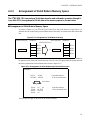
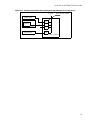
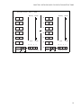
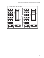
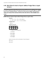
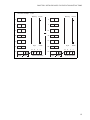
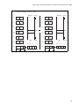
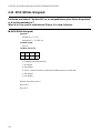
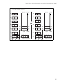
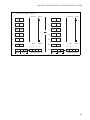
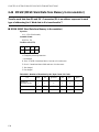
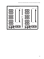
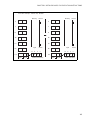
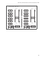
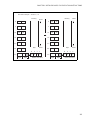
■ CPU Memory Space
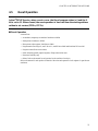
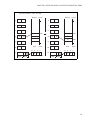
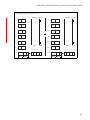
Figure 2.1-1 shows the address configuration of the F
2
MC-8FX memory space.
The I/O area is located close to the least significant address, and the data area is arranged right above it.
The data area can be divided into the register bank, stack and direct areas for each application. In contrast
to the I/O area, the program area is located close to the most significant address. The reset, interrupt reset
vector and vector call instruction tables are arranged in the highest part.
Figure 2.1-1 F
2
MC-8FX Memory Space
I/O
FFFFH
0000H
Program area
Data area

7
CHAPTER 2 MEMORY SPACE
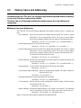
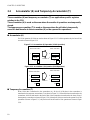
2.2 Memory Space and Addressing
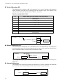
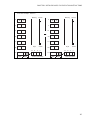
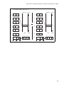
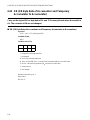
In addressing by the F
2
MC-8FX CPU, the applicable addressing mode related to memory
access may change according to the address.
Therefore, the use of the proper addressing mode increases the code efficiency of
instructions.
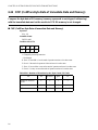
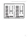
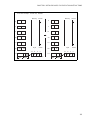
■ Memory Space and Addressing
The F
2
MC-8FX CPU has the following addressing modes related to memory access. ([ ] indicates one
byte):
• Direct addressing: Specify the lower 8 bits of the address using the operand. The accesses of operand
address 00
H
to 7F
H
are always 0000
H
to 007F
H
. The accesses of operand address
80
H
to FF
H
are mapped to 0080
H
to 047F
H
by setting of direct bank pointer (DP).
[Structure] [← OP code →] [← lower 8 bits →] ([← if operand available →]
• Extended addressing:Specify all 16 bits using the operand.
[Structure] [← OP code →] [← upper 8 bits →] [← lower 8 bits →]
• Bit direct addressing:Specify the lower 8 bits of the address using the operand. The accesses of operand
address 00
H
to 7F
H
are always 0000
H
to 007F
H
. The accesses of operand address
80
H
to FF
H
are mapped to 0080
H
to 047F
H
by setting of direct bank pointer (DP).
The bit positions are included in the OP code.
[Structure] [← OP code: bit →] [← lower 8 bits →]
• Indexed addressing: Add the 8 bits of the operand to the index register (IX) together with the sign and
use the result as the address.
[Structure] [← OP code →] [← 8 offset bits →] ([← if operand available →])
• Pointer addressing: Use the contents of the extra pointer (EP) directly as the address.
[Structure] [← OP code →]
• General-purpose register addressing: Specify the general-purpose registers. The register numbers are
included in the OP code.
[Structure] [← OP code: register →]
• Immediate addressing:Use one byte following the OP code as data.
[Structure] [← OP code →] [← Immediate data →]
• Vector addressing: Read the data from a table corresponding to the table number. The table numbers
are included in the OP code.
[Structure] [← OP code: table →]
• Relative addressing: Calculate the address relatively to the contents of the current PC. This addressing
mode is used during the execution of the relative jump and bit check instructions.
[Structure] [← OP code: table →] [← 8 bit relative value →]
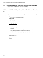
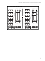
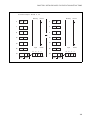
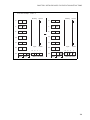
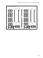
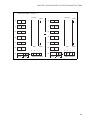
Figure 2.2-1 shows the memory space accessible by each addressing mode.

8
CHAPTER 2 MEMORY SPACE
Figure 2.2-1 Memory Space and Addressing
: Direct addressing
: Extended addressing
: Bit direct addressing
: Index addressing
: Pointer addressing
: General-purpose register addressing
: Immediate addressing
: Vector addressing
: Relative addressing
Interrupt vector
CALLV table
Program area
External area
Data area
Register bank
FFFF
H
FFD0
H
FFC0
H
0200
H
0100
H
0000
H
I/O area
+127 bytes
-128 bytes
047F
H
Page is loading ...
Page is loading ...
Page is loading ...
Page is loading ...
Page is loading ...
Page is loading ...
Page is loading ...
Page is loading ...
Page is loading ...
Page is loading ...
Page is loading ...
Page is loading ...
Page is loading ...
Page is loading ...
Page is loading ...
Page is loading ...
Page is loading ...
Page is loading ...
Page is loading ...
Page is loading ...
Page is loading ...
Page is loading ...
Page is loading ...
Page is loading ...
Page is loading ...
Page is loading ...
Page is loading ...
Page is loading ...
Page is loading ...
Page is loading ...
Page is loading ...
Page is loading ...
Page is loading ...
Page is loading ...
Page is loading ...
Page is loading ...
Page is loading ...
Page is loading ...
Page is loading ...
Page is loading ...
Page is loading ...
Page is loading ...
Page is loading ...
Page is loading ...
Page is loading ...
Page is loading ...
Page is loading ...
Page is loading ...
Page is loading ...
Page is loading ...
Page is loading ...
Page is loading ...
Page is loading ...
Page is loading ...
Page is loading ...
Page is loading ...
Page is loading ...
Page is loading ...
Page is loading ...
Page is loading ...
Page is loading ...
Page is loading ...
Page is loading ...
Page is loading ...
Page is loading ...
Page is loading ...
Page is loading ...
Page is loading ...
Page is loading ...
Page is loading ...
Page is loading ...
Page is loading ...
Page is loading ...
Page is loading ...
Page is loading ...
Page is loading ...
Page is loading ...
Page is loading ...
Page is loading ...
Page is loading ...
Page is loading ...
Page is loading ...
Page is loading ...
Page is loading ...
Page is loading ...
Page is loading ...
Page is loading ...
Page is loading ...
Page is loading ...
Page is loading ...
Page is loading ...
Page is loading ...
Page is loading ...
Page is loading ...
Page is loading ...
Page is loading ...
Page is loading ...
Page is loading ...
Page is loading ...
Page is loading ...
Page is loading ...
Page is loading ...
Page is loading ...
Page is loading ...
Page is loading ...
Page is loading ...
Page is loading ...
Page is loading ...
Page is loading ...
Page is loading ...
Page is loading ...
Page is loading ...
Page is loading ...
Page is loading ...
Page is loading ...
Page is loading ...
Page is loading ...
Page is loading ...
Page is loading ...
Page is loading ...
Page is loading ...
Page is loading ...
Page is loading ...
Page is loading ...
Page is loading ...
Page is loading ...
Page is loading ...
Page is loading ...
Page is loading ...
Page is loading ...
Page is loading ...
Page is loading ...
Page is loading ...
Page is loading ...
Page is loading ...
Page is loading ...
Page is loading ...
Page is loading ...
Page is loading ...
Page is loading ...
Page is loading ...
Page is loading ...
Page is loading ...
Page is loading ...
Page is loading ...
Page is loading ...
Page is loading ...
Page is loading ...
Page is loading ...
Page is loading ...
Page is loading ...
Page is loading ...
Page is loading ...
Page is loading ...
Page is loading ...
Page is loading ...
Page is loading ...
Page is loading ...
Page is loading ...
Page is loading ...
Page is loading ...
Page is loading ...
Page is loading ...
Page is loading ...
Page is loading ...
Page is loading ...
Page is loading ...
Page is loading ...
Page is loading ...
Page is loading ...
Page is loading ...
Page is loading ...
Page is loading ...
Page is loading ...
Page is loading ...
Page is loading ...
Page is loading ...
Page is loading ...
Page is loading ...
Page is loading ...
Page is loading ...
Page is loading ...
Page is loading ...
Page is loading ...
Page is loading ...
Page is loading ...
Page is loading ...
Page is loading ...
Page is loading ...
Page is loading ...
Page is loading ...
Page is loading ...
Page is loading ...
Page is loading ...
Page is loading ...
Page is loading ...
Page is loading ...
Page is loading ...
Page is loading ...
Page is loading ...
Page is loading ...
Page is loading ...
Page is loading ...
Page is loading ...
Page is loading ...
Page is loading ...
Page is loading ...
Page is loading ...
Page is loading ...
Page is loading ...
Page is loading ...
Page is loading ...
Page is loading ...
Page is loading ...
Page is loading ...
Page is loading ...
Page is loading ...
Page is loading ...
Page is loading ...
Page is loading ...
Page is loading ...
Page is loading ...
Page is loading ...
Page is loading ...
Page is loading ...
Page is loading ...
Page is loading ...
Page is loading ...
Page is loading ...
Page is loading ...
Page is loading ...
Page is loading ...
Page is loading ...
Page is loading ...
Page is loading ...
Page is loading ...
Page is loading ...
Page is loading ...
Page is loading ...
Page is loading ...
Page is loading ...
Page is loading ...
Page is loading ...
Page is loading ...
Page is loading ...
Page is loading ...
Page is loading ...
Page is loading ...
Page is loading ...
Page is loading ...
Page is loading ...
Page is loading ...
-
 1
1
-
 2
2
-
 3
3
-
 4
4
-
 5
5
-
 6
6
-
 7
7
-
 8
8
-
 9
9
-
 10
10
-
 11
11
-
 12
12
-
 13
13
-
 14
14
-
 15
15
-
 16
16
-
 17
17
-
 18
18
-
 19
19
-
 20
20
-
 21
21
-
 22
22
-
 23
23
-
 24
24
-
 25
25
-
 26
26
-
 27
27
-
 28
28
-
 29
29
-
 30
30
-
 31
31
-
 32
32
-
 33
33
-
 34
34
-
 35
35
-
 36
36
-
 37
37
-
 38
38
-
 39
39
-
 40
40
-
 41
41
-
 42
42
-
 43
43
-
 44
44
-
 45
45
-
 46
46
-
 47
47
-
 48
48
-
 49
49
-
 50
50
-
 51
51
-
 52
52
-
 53
53
-
 54
54
-
 55
55
-
 56
56
-
 57
57
-
 58
58
-
 59
59
-
 60
60
-
 61
61
-
 62
62
-
 63
63
-
 64
64
-
 65
65
-
 66
66
-
 67
67
-
 68
68
-
 69
69
-
 70
70
-
 71
71
-
 72
72
-
 73
73
-
 74
74
-
 75
75
-
 76
76
-
 77
77
-
 78
78
-
 79
79
-
 80
80
-
 81
81
-
 82
82
-
 83
83
-
 84
84
-
 85
85
-
 86
86
-
 87
87
-
 88
88
-
 89
89
-
 90
90
-
 91
91
-
 92
92
-
 93
93
-
 94
94
-
 95
95
-
 96
96
-
 97
97
-
 98
98
-
 99
99
-
 100
100
-
 101
101
-
 102
102
-
 103
103
-
 104
104
-
 105
105
-
 106
106
-
 107
107
-
 108
108
-
 109
109
-
 110
110
-
 111
111
-
 112
112
-
 113
113
-
 114
114
-
 115
115
-
 116
116
-
 117
117
-
 118
118
-
 119
119
-
 120
120
-
 121
121
-
 122
122
-
 123
123
-
 124
124
-
 125
125
-
 126
126
-
 127
127
-
 128
128
-
 129
129
-
 130
130
-
 131
131
-
 132
132
-
 133
133
-
 134
134
-
 135
135
-
 136
136
-
 137
137
-
 138
138
-
 139
139
-
 140
140
-
 141
141
-
 142
142
-
 143
143
-
 144
144
-
 145
145
-
 146
146
-
 147
147
-
 148
148
-
 149
149
-
 150
150
-
 151
151
-
 152
152
-
 153
153
-
 154
154
-
 155
155
-
 156
156
-
 157
157
-
 158
158
-
 159
159
-
 160
160
-
 161
161
-
 162
162
-
 163
163
-
 164
164
-
 165
165
-
 166
166
-
 167
167
-
 168
168
-
 169
169
-
 170
170
-
 171
171
-
 172
172
-
 173
173
-
 174
174
-
 175
175
-
 176
176
-
 177
177
-
 178
178
-
 179
179
-
 180
180
-
 181
181
-
 182
182
-
 183
183
-
 184
184
-
 185
185
-
 186
186
-
 187
187
-
 188
188
-
 189
189
-
 190
190
-
 191
191
-
 192
192
-
 193
193
-
 194
194
-
 195
195
-
 196
196
-
 197
197
-
 198
198
-
 199
199
-
 200
200
-
 201
201
-
 202
202
-
 203
203
-
 204
204
-
 205
205
-
 206
206
-
 207
207
-
 208
208
-
 209
209
-
 210
210
-
 211
211
-
 212
212
-
 213
213
-
 214
214
-
 215
215
-
 216
216
-
 217
217
-
 218
218
-
 219
219
-
 220
220
-
 221
221
-
 222
222
-
 223
223
-
 224
224
-
 225
225
-
 226
226
-
 227
227
-
 228
228
-
 229
229
-
 230
230
-
 231
231
-
 232
232
-
 233
233
-
 234
234
-
 235
235
-
 236
236
-
 237
237
-
 238
238
-
 239
239
-
 240
240
-
 241
241
-
 242
242
-
 243
243
-
 244
244
-
 245
245
-
 246
246
-
 247
247
-
 248
248
-
 249
249
-
 250
250
-
 251
251
-
 252
252
-
 253
253
-
 254
254
-
 255
255
-
 256
256
-
 257
257
-
 258
258
-
 259
259
-
 260
260
-
 261
261
-
 262
262
-
 263
263
-
 264
264
-
 265
265
-
 266
266
-
 267
267
-
 268
268
-
 269
269
-
 270
270
-
 271
271
-
 272
272


Ask a question and I''ll find the answer in the document
Finding information in a document is now easier with AI
Related papers
-
Fujitsu F202RA User manual
-
-
-
-
Fujitsu F2 MC-16 User manual
-
-
-
-
-
Other documents
-
Hitachi H8/300L Series Programming Manual
-
Texas Instruments TMS320C55x DSP Mnemonic Set (Rev. G) User guide
-
NXP S12XD Reference guide
-
-
-
-
Motorola CPU12 Refrence Manual
-
NXP 68HC912D60C Reference guide
-
Freescale Semiconductor S12T Reference guide
-
Toshiba TMP87CM24AF User manual