Page is loading ...

www.omega.com
e-mail: [email protected]
User’s Guide
OME-PIO-D56/D24
PCI-Bus
Digital I/O Board
Hardware Manual
Shop online at

Servicing North America:
USA: One Omega Drive, P.O. Box 4047
ISO 9001 Certified Stamford CT 06907-0047
TEL: (203) 359-1660 FAX: (203) 359-7700
e-mail: [email protected]
Canada: 976 Bergar
Laval (Quebec) H7L 5A1, Canada
TEL: (514) 856-6928 FAX: (514) 856-6886
e-mail: [email protected]
For immediate technical or application assistance:
USA and Canada: Sales Service: 1-800-826-6342 / 1-800-TC-OMEGA
®
Customer Service: 1-800-622-2378 / 1-800-622-BEST
®
Engineering Service: 1-800-872-9436 / 1-800-USA-WHEN
®
TELEX: 996404 EASYLINK: 62968934 CABLE: OMEGA
Mexico: En Espan˜ol: (001) 203-359-7803 e-mail: [email protected]
FAX: (001) 203-359-7807 [email protected]
Servicing Europe:
Benelux: Postbus 8034, 1180 LA Amstelveen, The Netherlands
TEL: +31 (0)20 3472121 FAX: +31 (0)20 6434643
Toll Free in Benelux: 0800 0993344
e-mail: [email protected]
Czech Republic: Frystatska 184, 733 01 Karviná, Czech Republic
TEL: +420 (0)59 6311899 FAX: +420 (0)59 6311114
Toll Free: 0800-1-66342 e-mail: [email protected]
France: 11, rue Jacques Cartier, 78280 Guyancourt, France
TEL: +33 (0)1 61 37 29 00 FAX: +33 (0)1 30 57 54 27
Toll Free in France: 0800 466 342
e-mail: [email protected]
Germany/Austria: Daimlerstrasse 26, D-75392 Deckenpfronn, Germany
TEL: +49 (0)7056 9398-0 FAX: +49 (0)7056 9398-29
Toll Free in Germany: 0800 639 7678
e-mail: [email protected]
United Kingdom: One Omega Drive, River Bend Technology Centre
ISO 9002 Certified Northbank, Irlam, Manchester
M44 5BD United Kingdom
TEL: +44 (0)161 777 6611 FAX: +44 (0)161 777 6622
Toll Free in United Kingdom: 0800-488-488
e-mail: [email protected]
OMEGAnet
®
Online Service Internet e-mail
www.omega.com [email protected]
It is the policy of OMEGA to comply with all worldwide safety and EMC/EMI regulations that
apply. OMEGA is constantly pursuing certification of its products to the European New Approach
Directives. OMEGA will add the CE mark to every appropriate device upon certification.
The information contained in this document is believed to be correct, but OMEGA Engineering, Inc. accepts
no liability for any errors it contains, and reserves the right to alter specifications without notice.
WARNING: These products are not designed for use in, and should not be used for, patient-connected applications.

OME-PIO-D56/D24
User Manual
OME-PIO-D56/OME-PIO-D24 User Manual (Ver.2.1, Oct/2003) ---- 1

Table of Contents
1. INTRODUCTION...........................................................................................................................3
1.1 FEATURES ....................................................................................................................................3
1.2 SPECIFICATIONS ...........................................................................................................................4
1.3 ORDER DESCRIPTION....................................................................................................................4
1.4 PCI DATA ACQUISITION FAMILY .................................................................................................5
1.5 PRODUCT CHECKLIST ...................................................................................................................5
2. HARDWARE CONFIGURATION...............................................................................................6
2.1 BOARD LAYOUT ...........................................................................................................................6
2.2 I/O PORT LOCATION.....................................................................................................................7
2.3 ENABLING I/O OPERATION...........................................................................................................7
2.4 INTERRUPT OPERATION ..............................................................................................................11
2.5 DAUGHTER BOARDS...................................................................................................................18
2.6 PIN ASSIGNMENT........................................................................................................................24
3. I/O CONTROL REGISTER ........................................................................................................26
3.1 HOW TO FIND THE I/O ADDRESS ................................................................................................26
3.2 THE ASSIGNMENT OF I/O ADDRESS.............................................................................................32
3.3 THE I/O ADDRESS MAP ..............................................................................................................33
4. DEMO PROGRAM ......................................................................................................................38
4.1 PIO_PISO..................................................................................................................................39
4.2 DEMO1 .....................................................................................................................................41
4.3 DEMO2 .....................................................................................................................................42
4.4 DEMO3 .....................................................................................................................................43
4.5 DEMO4 .....................................................................................................................................45
4.6 DEMO5 .....................................................................................................................................47
OME-PIO-D56/OME-PIO-D24 User Manual (Ver.2.1, Oct/2003, PPH-005-21) ---- 2

1. Introduction
The OME-PIO-D56/OME-OME-PIO-D24 provides 56/24 TTL digital I/O lines.
The OME-PIO-D56/OME-OME-PIO-D24 consists of one 24-bit bi-directional port,
one 16-bit input port and one 16-bit output port (only for OME-PIO-D56). The 24-bit
port supports three 8-bit groups PA, PB & PC. Each 8-bit group can be individually
configured to function as either an input or an output. All groups using 24-bit bi-
directional ports are configured as inputs upon power-up or reset.
Use the OME-DB-24PD to connect the input port for either isolation purposes,
or to interface to the output port for relay control. The OME-PIO-D56/OME-PIO-D24
has one D-sub connector and two 20-pin flat-cable connectors (only for OME-PIO-
D56). The flat cable can be connected to an OME-ADP-20/PCI adapter. The adapter
can be fixed on the chassis. It can be installed in a 5V PCI bus and supports “Plug &
Play”.
1.1 Features
• PCI bus
• Up to 56/24(OME-PIO-D56/OME-PIO-D24) channels of digital I/O
• All I/O lines buffered on the board
• Eight-bit groups independently selectable for I/O on 24-bit port
• Input / Output programmable I/O ports under software control
• Double side SMD, short card.
• Connects directly to OME-DB-24PR, OME-DB-24PD, OME-DB-24RD,
OME-DB-24PRD, OME-DB-16P8R, OME-DB-24POR, OME-DB-24SSR or
OME-DB-24C
• 4 interrupt sources: PC0, PC1, PC2, PC3
• One DB37 connector, two 20-pin flat-cable connectors (only for OME-PIO-D56)
• High drive capability
• Automatically detected by Windows 95/98/2000/XP
• No base address or IRQ switches to set
OME-PIO-D56/OME-PIO-D24 User Manual (Ver.2.1, Oct/2003) ---- 3

1.2 Specifications
• All inputs are TTL compatible
Logic high voltage : 2.4V (Min.)
Logic low voltage : 0.8V (Max.)
• All outputs are TTL compatible
OPTO-22 output (CON3)
Sink current : 64mA (Max.)
Source current : 32mA(Max.)
16-channel output (CON1)
Sink current : 8mA (Max.)
Source current : 0.4mA(Max.)
• Environmental :
Operating Temperature: 0°C to 60°C
Storage Temperature: -20°C to 80°C
Humidity: 0 to 90% non-condensing
• Dimensions: 143mm X 105mm
• Power Consumption: +5V @ 530mA/420mA(OME-PIO-D56/OME-PIO-D24)
1.3 Order Description
• OME-PIO-D56 : PCI bus 56-bit DI/O board
• OME-PIO-D24 : PCI bus 24-bit DI/O board
1.3.1 Options
• OME-DB-24PD : 24 channel isolated D/I board
• OME-DB-24RD : 24 channel relay board
• OME-DB-24PRD : 24 channel power relay board
• OME-DB-16P8R : 16 channel isolated D/I and 8 channels relay output board
• OME-DB-24POR : 24 channel Photo MOS output board
• OME-DB-24C : 24 channel open-collector output board
• OME-ADP-20/PCI : extender, 20-pin header to 20-pin header for PCI bus I/O
boards
OME-PIO-D56/PIO-D24 User Manual (Ver.2.1, Oct/2003, PPH-005-21) ---- 4

1.4 PCI Data Acquisition Family
We provide a family of PCI bus data acquisition cards. These cards can be
divided into three groups as follows:
1. OME-PCI-series: first generation, isolated or non-isolated cards
OME-PCI-1002/1202/1800/1802/1602: multi-function family, non-isolated
OME-PCI-P16R16/P16C16/P16POR16/P8R8: D/I/O family, isolated
OME-PCI-TMC12: timer/counter card, non-isolated
2. OME-PIO-series: cost-effective generation, non-isolated cards
OME-PIO-823/821: multi-function family
OME-PIO-D144/D96/D64/D56/D48/D24: D/I/O family
OME-PIO-DA16/DA8/DA4: D/A family
3. OME-PISO-series: cost-effective generation, isolated cards
OME-PISO-813: A/D card
OME-PISO-P32C32/P64/C64: D/I/O family
OME-PISO-P8R8/P8SSR8AC/P8SSR8DC: D/I/O family
OME-PISO-730: D/I/O card
OME-PISO-DA2: D/A card
1.5 Product Checklist
In addition to this manual, the package includes the following items:
• One OME-PIO-D56(or OME-PIO-D24) card
• One software floppy diskette or CD
• One release note
Please read the release note first. Important information that could be given in release
note such as:
1. Where you can find the software driver & utility?
2. How to install software & utility?
3. The location of the diagnostic program?
4. FAQ
Attention!
If any one of these items is missing or damaged, please contact
Omega Engineering immediately. Save the shipping materials
and carton in case you want to ship or store the product in the
future.
OME-PIO-D56/OME-PIO-D24 User Manual (Ver.2.1, Oct/2003) ---- 5
2. Hardware configuration
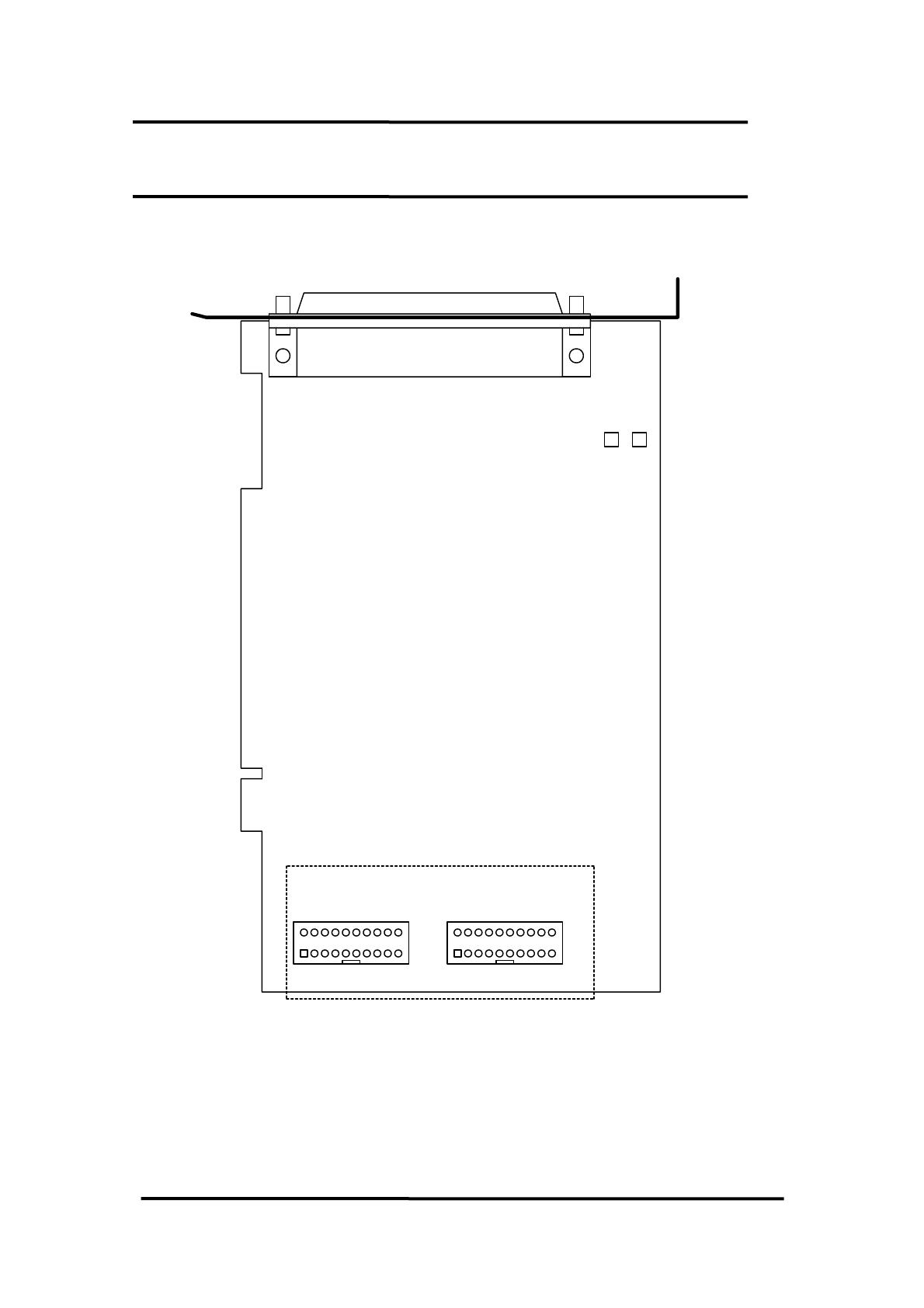
2.1 Board Layout
CON1
CON2
CON3
PCI BUS
PIO-D56
PIO-D24
12
1920
12
1920
D/I
D/O
DI/O
Port0
Port1
Port2
only for PIO-D56
OME-PIO-D56/PIO-D24 User Manual (Ver.2.1, Oct/2003, PPH-005-21) ---- 6

2.2 I/O Port Location
The OME-PIO-D56/OME-PIO-D24 consists of one 24-bit bi-directional port, one
16 bit input port and one 16 bit output port (only for OME-PIO-D56). The 24-bit port
supports three 8-bit groups: PA, PB & PC. Each 8-bit group can be individually
configured to function as either inputs or outputs. All groups using 24-bit bi-
directional ports are configured as inputs upon power-up or reset. The I/O port
locations are as follows:
Connector of
OME-PIO-D56/D24
PA0 ~ PA7 PB0 ~ PB7 PC0 ~ PC7
CON3 (DI/O) Port0 Port1 Port2
Connector of OME-PIO-D56 Description
CON1 D/O
CON2 D/I
Refer to Sec. 2.1 for board layout & I/O port location.
Note: PC0, PC1, PC2 and PC3 can be used as interrupt signal source. Refer to Sec.
2.4 for more information.
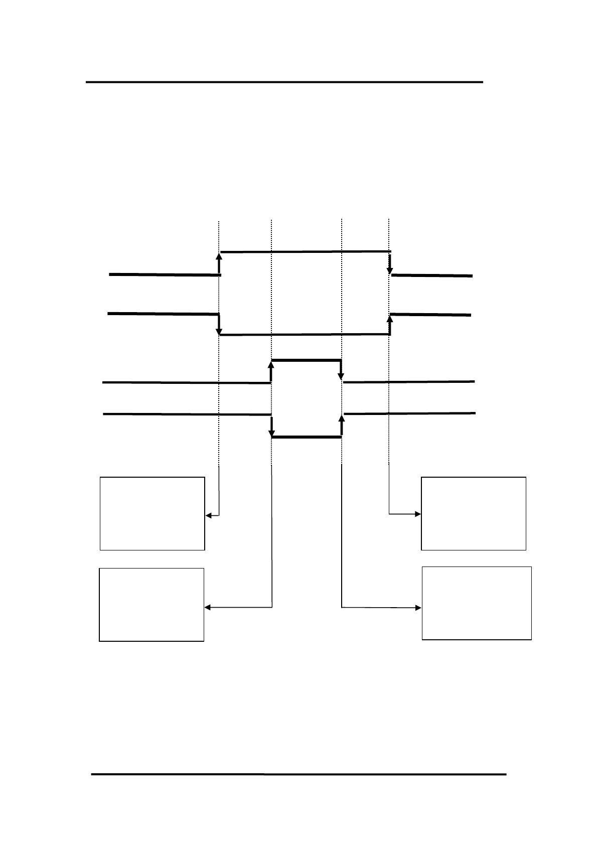
2.3 Enabling I/O Operation
2.3.1 DI/DO Port Architecture (CON3)
Upon power-up, all D/I/O port (CON3) operations are disabled. The RESET\
signal controls the enable/disable state of D/I/O port. Refer to Sec. 3.3.1 for more
information about RESET\ signal. The power-up states are as follows:
• All D/I/O operations are disabled
• All three D/I/O ports are configured as D/I port
• All D/O latch register are undefined.(refer to Sec. 2.3.2)
Initialization must be performed before using these D/I/Os. The recommended
steps are as follows:
Step 1: Find address-mapping of OME-PIO/PISO cards (refer to Sec. 3.1)
Step 2: Enable all D/I/O operations (refer to Sec. 3.3.1)
Step 3: Configure the three ports (in CON3) to their expected D/I/O state &
send the initial value to all D/O ports (refer to Sec. 3.3.8)
Refer to DEMO1.C for demo program.
OME-PIO-D56/OME-PIO-D24 User Manual (Ver.2.1, Oct/2003) ---- 7

I/O select (Sec. 3.3.7)
disable\
input Latch
Clock input
D/O latch CKT
RESET\ (Sec. 3.3.1)
Data
(Sec. 3.3.8)
D/I/O
disable
Buffer input
Clock input
D/I buffer CKT
Data
(Sec. 3.3.8)
• When the RESET\ is in Low-state Æ all D/I/O operations are disabled
• When the RESET\ is in High-state Æ all D/I/O operation are enabled.
• If D/I/O is configured as D/I port Æ D/I= external input signal
• If D/I/O is configured as D/O port Æ D/I = read back of D/O
• If D/I/O is configured as D/I port Æ send to D/O will change the D/O latch
register only. The D/I & external input signals will not change.
OME-PIO-D56/PIO-D24 User Manual (Ver.2.1, Oct/2003, PPH-005-21) ---- 8

2.3.2 DI Port Architecture (CON2)
When the PC is powered up, all DI (CON2) port operations are disabled. The
RESET\ signal controls the enable/disable signal for the DI port. Refer to Sec. 3.3.1
for more information about the RESET\ signal.
• The RESET\ is in Low-state Æ all DI operations are disabled
• The RESET\ is in High-state Æ all DI operations are enabled
D/I buffer CKT
Clock input
Buffer input
Data
RESET\
CON2
disable
OME-PIO-D56/OME-PIO-D24 User Manual (Ver.2.1, Oct/2003) ---- 9

2.3.3 DO Port Architecture (CON1)
When the PC is powered up, all DO port (CON1) operations are disabled. The
RESET\ signal controls the enable/disable signal for the DI port. Refer to Sec. 3.3.1
for more information about the RESET\ signal.
• The RESET\ is in Low-state Æ all DO operations are disabled
• The RESET\ is in High-state Æ all DO operations are enabled
The power-up states are as follows:
• All DO operations are disabled
• All output latches are cleared to Low-Level
D/O buffer CKT
Clock input
input Latch
Data
RESET\
CON1
clear
OME-PIO-D56/PIO-D24 User Manual (Ver.2.1, Oct/2003, PPH-005-21) ---- 10

2.4 Interrupt Operation
All PC0, PC1, PC2 and PC3 can be used as an interrupt signal sources. Refer to
Sec. 2.1 for PC0/PC1/PC2/PC3 location. The interrupt of OME-PIO-D56/OME-
PIO-D24 is level-trigger & Active_High. The interrupt signal can be programmed to
inverted or non-inverted state. The programming procedure is given as follows:
1. Make sure the initial level is High or Low
2. If the initial state is High Æ select the inverted signal (Sec. 3.3.6)
3. If the initial state is Low Æ select the
non-inverted signal (Sec. 3.3.6)
4. Enable the INT function (Sec. 3.3.4)
5. If the interrupt signal is active Æ program will transfer into the interrupt
service routine Æ if INT signal is High now Æ select the inverted input
Æ if INT signal is Low now Æ select the non-inverted input
Refer to DEMO3.C & DEMO4.C for single interrupt source. Refer to
DEMO5.C for four interrupt sources.
If only one interrupt signal source is used, the interrupt service routine does not
have to identify the interrupt source. (Refer to DEMO3.C & DEMO4.C)
If there is more than one interrupt source, the interrupt service routine has to
identify the active signals via the following steps: (Refer to DEMO5.C)
1. Reads the new status of the interrupt signal source
2. Compares the new status with the old status to identify the active signals
3. If PC0 is active, service PC0 & non-inverter/inverted the PC0 signal
4. If PC1 is active, service PC1 & non-inverted/inverted the PC1 signal
5. If PC2 is active, service PC2 & non-inverted/inverted the PC2 signal
6. If PC3 is active, service PC3 & non-inverted/inverted the PC3 signal
7. Saves the new status to old status
Note: If the interrupt signal is too short, the new status may be the same as old
status. So the interrupt signal must be held active until the interrupt service
routine is executed. This hold time is different for different operating systems. It
can be as a short as micro-second or as a long as second. In general, 20ms is
enough for most operating systems.
OME-PIO-D56/OME-PIO-D24 User Manual (Ver.2.1, Oct/2003) ---- 11

2.4.1 Interrupt Block Diagram of OME-PIO-
D56/D24
INT_CHAN_0
INT_CHAN_1
INT_CHAN_2
INT_CHAN_3
INT\
Level_trigger
initial_low
active_high
The interrupt output signal of OME-PIO-D56/OME-PIO-D24, INT\ is
Level_trigger & Active_Low. If the INT\ generates a low pulse, the OME-PIO-
D56/OME-PIO-D24 will interrupt the PC only once. If the INT\ is fixed in low level,
the OME-PIO-D56/OME-PIO-D24 will interrupt the PC continuously.
INT_CHAN_0/1/2/3 must be controlled in a pulse type signals. It must be fixed in
low level state normally and generate a high pulse to interrupt the PC.
The priority of INT_CHAN_0/1/2/3 is the same. If all these four signals are active
at the same time, then INT\ will be active only one time. So the interrupt service
routine has to read the status of all interrupt channels for a multi-channel interrupt.
Refer to Sec. 2.4 for mare information.
DEMO5.C → for multi-channel interrupt source
If only one interrupt source is used, the interrupt service routine does not have to read
the status of interrupt source. The demo programs DEMO3.C and DEMO4.C are
designed for single-channel interrupt demo, as follows:
DEMO3.C → for INT_CHAN_0 only (PC0 initial low)
DEMO4.C → for INT_CHAN_0 only (PC0 initial high)
OME-PIO-D56/PIO-D24 User Manual (Ver.2.1, Oct/2003, PPH-005-21) ---- 12

2.4.2 INT_CHAN_0/1/2/3
INT_CHAN_0 (1/2/3)
Inverted/Noninverted select
INV0(1/2/3)
Enable/Disable select
EN0(1/2/3)
PC0(PC1/PC2/PC3)
The INT_CHAN_0 must normally be fixed in low level state and generate a
high pulse to interrupt the PC.
The EN0 (EN1/EN2/EN3) can be used to enable/disable the INT_CHAN_0(1/2/3)
as follows : (Refer to Sec. 3.3.4)
EN0 (1/2/3) = 0 → INT_CHAN_0(1/2/3) = disable
EN0 (1/2/3) = 1 → INT_CHAN_0(1/2/3) = enable
The INV0 can be used to invert/non-invert the PC0 (1/2/3) as follows: (Refer to
Sec.3.3.6)
INV0 (1/2/3) = 0 → INT_CHAN_0(1/2/3) = inverted state of PC0 (1/2/3)
INV0 (1/2/3) = 1 → INT_CHAN_0(1/2/3) = non-inverted state of PC0 (1/2/3)
OME-PIO-D56/OME-PIO-D24 User Manual (Ver.2.1, Oct/2003) ---- 13

2.4.3 Initial_high, active_low Interrupt source
If the PC0 is a initial_high, active_low signal, the interrupt service routine
should use INV0 to invert/non-invert the PC0 for high_pulse generation as follows:
(Refer to DEMO4.C)
Initial setting:
now_int_state=1; /* initial state for PC0 */
outportb(wBase+0x2a,0); /* select the inverted PC0 */
void interrupt irq_service()
{
if (now_int_state==1) /* now PC0 is changed to LOW */(a)
{ /* --> INT_CHAN_0=!PC0=HIGH now */
COUNT_L++; /* find a LOW_pulse (PC0) */
If((inport(wBase+7)&1)==0)/* the PC0 is still fixed in LOW */
{ /* Æ need to generate a high_pulse */
outportb(wBase+0x2a,1);/* INV0 select the non-inverted input */(b)
/* INT_CHAN_0=PC0=LOW --> */
/* INT_CHAN_0 generate a high_pulse */
now_int_state=0; /* now PC0=LOW */
}
else now_int_state=1; /* now PC0=HIGH */
/* don’t have to generate high_pulse */
}
else /* now PC0 is changed to HIGH */(c)
{ /* --> INT_CHAN_0=PC0=HIGH now */
COUNT_H++; /* find a HIGH_pulse (PC0) */
If((inport(wBase+7)&1)==1)/* the PC0 is still fixed in HIGH */
{ /* need to generate a high_pulse */
outportb(wBase+0x2a,0);/* INV0 select the inverted input */(d)
/* INT_CHAN_0=!PC0=LOW --> */
/* INT_CHAN_0 generate a high_pulse */
now_int_state=1; /* now PC0=HIGH */
}
else now_int_state=0; /* now PC0=LOW */
/* don’t have to generate high_pulse */
}
if (wIrq>=8) outportb(A2_8259,0x20);
outportb(A1_8259,0x20);
}
PC0
INV0
INT_CHAN_0
(a) (b) (c) (d)
OME-PIO-D56/PIO-D24 User Manual (Ver.2.1, Oct/2003, PPH-005-21) ---- 14

2.4.4 Initial_low, active_high Interrupt source
If the PC0 is a initial_low, active_high signal, the interrupt service routine
should use INV0 to inverted/non-inverted the PC0 for high_pulse generation as
follows: (Refer to DEMO3.C)
Initial setting:
now_int_state=0; /* initial state for PC0 */
outportb(wBase+0x2a,1); /* select the non-inverted PC0 */
void interrupt irq_service()
{
if (now_int_state==1) /* now PC0 is changed to LOW */(c)
{ /* --> INT_CHAN_0=!PC0=HIGH now */
COUNT_L++; /* find a LOW_pulse (PC0) */
If((inport(wBase+7)&1)==0)/* the PC0 is still fixed in LOW */
{ /* Æ need to generate a high_pulse */
outportb(wBase+0x2a,1);/* INV0 select the non-inverted input */(d)
/* INT_CHAN_0=PC0=LOW --> */
/* INT_CHAN_0 generate a high_pulse */
now_int_state=0; /* now PC0=LOW */
}
else now_int_state=1; /* now PC0=HIGH */
/* don’t have to generate high_pulse */
}
else /* now PC0 is changed to HIGH */(a)
{ /* --> INT_CHAN_0=PC0=HIGH now */
COUNT_H++; /* find a High_pulse (PC0) */
If((inport(wBase+7)&1)==1)/* the PC0 is still fixed in HIGH */
{ /* need to generate a high_pulse */
outportb(wBase+0x2a,0);/* INV0 select the inverted input */(b)
/* INT_CHAN_0=!PC0=LOW --> */
/* INT_CHAN_0 generate a high_pulse */
now_int_state=1; /* now PC0=HIGH */
}
else now_int_state=0; /* now PC0=LOW */
/* don’t have to generate high_pulse */
}
if (wIrq>=8) outportb(A2_8259,0x20);
outportb(A1_8259,0x20);
}
PC0
INV0
INT_CHAN_0
(a) (b) (c) (d)
OME-PIO-D56/OME-PIO-D24 User Manual (Ver.2.1, Oct/2003) ---- 15
2.4.5 Muliti-Interrupt Source
Assume: PC0 is initial Low, active High,
PC1 is initial High, active Low
PC2 is initial Low, active High
PC3 is initial High, active Low
as follows :
PC1
PC0
PC2
PC3
PC0 & PC1 are
return to normal
at the same time.
PC2 & PC3 are
return to normal at
the same time.
PC0 & PC1 are
active at the same
time.
PC2 & PC3 are
active at the same
time.
Refer to DEMO5.C for source program. All these four falling-edge & rising-edge
can be detected by DEMO5.C.
Note: When the interrupt is active, the user program has to identify the active
signals. These signals may be active at the same time. The interrupt service
routine has to service all active signals at the same time.
OME-PIO-D56/PIO-D24 User Manual (Ver.2.1, Oct/2003, PPH-005-21) ---- 16

void interrupt irq_service()
{
new_int_state=inportb(wBase+7)&0x0f; /* read all interrupt state */
int_c=new_int_state^now_int_state; /* compare which interrupt */
/* signal be change */
if ((int_c&0x1)!=0) /* INT_CHAN_0 is active */
{
if ((new_int_state&0x01)!=0) /* now PC0 change to high */
{
CNT_H1++;
}
else /* now PC0 change to low */
{
CNT_L1++;
}
invert=invert^1; /* to generate a high pulse */
}
if ((int_c&0x2)!=0)
{
if ((new_int_state&0x02)!=0) /* now PC1 change to high */
{
CNT_H2++;
}
else /* now PC1 change to low */
{
CNT_L2++;
{
invert=invert^2; /* to generate a high pulse */
}
if ((int_c&0x4)!=0)
{
If ((new_int_state&0x04)!=0) /* now PC2 change to high */
{
CNT_H3++;
}
else /* now PC2 change to low */
{
CNT_L3++;
}
invert=invert^4; /* to generate a high pulse */
}
if ((int_c&0x8)!=0)
{
if ((new_int_state&0x08)!=0) /* now PC3 change to high */
{
CNT_H4++;
{
else /* now PC3 change to low */
{
CNT_L4++;
}
invert=invert^8; /* to generate a high pulse */
}
now_int_state=new_int_state;
outportb(wBase+0x2a,invert);
if (wIrq>=8) outportb(A2_8259,0x20);
outportb(A1_8259,0x20);
}
OME-PIO-D56/OME-PIO-D24 User Manual (Ver.2.1, Oct/2003) ---- 17

2.5 Daughter Boards
2.5.1 OME-DB-37
The OME-DB-37 is a general purpose daughter board for D-sub 37 pins,
designed for an easy-wiring connection.
2.5.2 OME-DN-37
The OME-DN-37 is a general purpose daughter board for OME-DB-37 with DIN-
Rail Mounting. It is designed for easy-wiring connection..
37pin cable
2.5.3 OME-DB-8125
OME-DN-37
The OME-DB-8125 is a general purpose screw terminal board. It is designed for
easy wire connection. There is one D-Sub37 & two 20-pin flat-cable headers on the
OME-DB-8125.
37pin cable
OME-DB-8125
(D-Sub 37 or
20-
p
in flat-cable header
)
OME-PIO-D56/PIO-D24 User Manual (Ver.2.1, Oct/2003, PPH-005-21) ---- 18
/