
Document Number: 324642-003
2nd Generation Intel
®
Core™ Processor Family Desktop,
Intel
®
Pentium
®
Processor Family Desktop, and
Intel
®
Celeron
®
Processor Family Desktop
Datasheet, Volume 2
Supporting:
Intel
®
Core™ i7, i5 and i3 Desktop Processor Series
Intel
®
Pentium
®
G800 and G600 Desktop Processor Series
Intel
®
Celeron
®
G500 and G400 Desktop Processor Series
This is Volume 2 of 2
September 2011

2 Datasheet, Volume 2
Legal Lines and Disclaimers
INFORMATION IN THIS DOCUMENT IS PROVIDED IN CONNECTION WITH INTEL PRODUCTS. NO LICENSE, EXPRESS OR IMPLIED,
BY ESTOPPEL OR OTHERWISE, TO ANY INTELLECTUAL PROPERTY RIGHTS IS GRANTED BY THIS DOCUMENT. EXCEPT AS
PROVIDED IN INTEL'S TERMS AND CONDITIONS OF SALE FOR SUCH PRODUCTS, INTEL ASSUMES NO LIABILITY WHATSOEVER
AND INTEL DISCLAIMS ANY EXPRESS OR IMPLIED WARRANTY, RELATING TO SALE AND/OR USE OF INTEL PRODUCTS INCLUDING
LIABILITY OR WARRANTIES RELATING TO FITNESS FOR A PARTICULAR PURPOSE, MERCHANTABILITY, OR INFRINGEMENT OF ANY
PATENT, COPYRIGHT OR OTHER INTELLECTUAL PROPERTY RIGHT.
UNLESS OTHERWISE AGREED IN WRITING BY INTEL, THE INTEL PRODUCTS ARE NOT DESIGNED NOR INTENDED FOR ANY
APPLICATION IN WHICH THE FAILURE OF THE INTEL PRODUCT COULD CREATE A SITUATION WHERE PERSONAL INJURY OR DEATH
MAY OCCUR.
Intel may make changes to specifications and product descriptions at any time, without notice. Designers must not rely on the
absence or characteristics of any features or instructions marked "reserved" or "undefined." Intel reserves these for future
definition and shall have no responsibility whatsoever for conflicts or incompatibilities arising from future changes to them. The
information here is subject to change without notice. Do not finalize a design with this information.
The products described in this document may contain design defects or errors known as errata which may cause the product to
deviate from published specifications. Current characterized errata are available on request.
Contact your local Intel sales office or your distributor to obtain the latest specifications and before placing your product order.
Copies of documents which have an order number and are referenced in this document, or other Intel literature, may be obtained
at: http://www.intel.com/design/literature.htm
All products, platforms, dates, and figures specified are preliminary based on current expectations, and are subject to change
without notice. All dates specified are target dates, are provided for planning purposes only and are subject to change.
This document contains information on products in the design phase of development. Do not finalize a design with this information.
Revised information will be published when the product is available. Verify with your local sales office that you have the latest
datasheet before finalizing a design.
Designers must not rely on the absence or characteristics of any features or instructions marked “reserved” or “undefined.” Intel
reserves these for future definition and shall have no responsibility whatsoever for conflicts or incompatibilities arising from future
changes to them.
The products described in this document may contain design defects or errors known as errata which may cause the product to
deviate from published specifications. Current characterized errata are available on request.
Intel processor numbers are not a measure of performance. Processor numbers differentiate features within each processor
family, not across different processor families. See http://www.intel.com/products/processor_number for details. Over time
processor numbers will increment based on changes in clock, speed, cache, FSB, or other features, and increments are not
intended to represent proportional or quantitative increases in any particular feature. Current roadmap processor number
progression is not necessarily representative of future roadmaps. See www.intel.com/products/processor_number for details.
No computer system can provide absolute security under all conditions. Intel
®
Trusted Execution Technology (Intel
®
TXT) requires
a computer system with Intel
®
Virtualization Technology, an Intel TXT-enabled processor, chipset, BIOS, Authenticated Code
Modules and an Intel TXT-compatible measured launched environment (MLE). The MLE could consist of a virtual machine monitor,
an OS or an application. In addition, Intel TXT requires the system to contain a TPM v1.2, as defined by the Trusted Computing
Group and specific software for some uses. For more information, see http://www.intel.com/technology/security/.
Intel
®
Virtualization Technology requires a computer system with an enabled Intel
®
processor, BIOS, virtual machine monitor
(VMM) and, for some uses, certain platform software enabled for it. Functionality, performance or other benefits will vary
depending on hardware and software configurations and may require a BIOS update. Software applications may not be compatible
with all operating systems. Please check with your application vendor.
Intel
®
Active Management Technology (Intel
®
AMT) requires the computer system to have an Intel
®
AMT-enabled chipset, network
hardware and software, as well as connection with a power source and a corporate network connection. Setup requires
configuration by the purchaser and may require scripting with the management console or further integration into existing security
frameworks to enable certain functionality. It may also require modifications of implementation of new business processes. With
regard to notebooks, Intel AMT may not be available or certain capabilities may be limited over a host OS-based VPN or when
connecting wirelessly, on battery power, sleeping, hibernating or powered off. For more information, see
http://www.intel.com/technology/platform-technology/intel-amt/
Enabling Execute Disable Bit functionality requires a PC with a processor with Execute Disable Bit capability and a supporting
operating system. Check with your PC manufacturer on whether your system delivers Execute Disable Bit functionality.
Intel, Pentium, Celeron, Intel Core, and the Intel logo are trademarks of Intel Corporation in the U. S. and other countries.
*Other names and brands may be claimed as the property of others.
Copyright © 2011 Intel Corporation. All Rights Reserved.

Datasheet, Volume 2 3
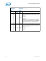
Contents
1Introduction............................................................................................................11
2 Processor Configuration Registers...........................................................................13
2.1 Register Terminology.........................................................................................13
2.2 PCI Devices and Functions on Processor ...............................................................14
2.3 System Address Map .........................................................................................15
2.3.1 Legacy Address Range.........................................................................18
2.3.1.1 DOS Range (0h–9_FFFFh)..........................................................18
2.3.1.2 Legacy Video Area (A_0000h–B_FFFFh) .......................................19
2.3.1.3 PAM (C_0000h–F_FFFFh)...........................................................20
2.3.2 Main Memory Address Range (1 MB – TOLUD).........................................20
2.3.2.1 ISA Hole (15 MB–16 MB) ...........................................................21
2.3.2.2 TSEG ......................................................................................21
2.3.2.3 Protected Memory Range (PMR) – (programmable) .......................21
2.3.2.4 DRAM Protected Range (DPR).....................................................22
2.3.2.5 Pre-allocated Memory ...............................................................22
2.3.2.6 Graphics Stolen Spaces .............................................................23
2.3.2.7 Intel
®
Management Engine (Intel ME) UMA .................................23
2.3.3 PCI Memory Address Range (TOLUD – 4 GB)...........................................23
2.3.3.1 APIC Configuration Space (FEC0_0000h–FECF_FFFFh) ...................25
2.3.3.2 HSEG (FEDA_0000h–FEDB_FFFFh)..............................................25
2.3.3.3 MSI Interrupt Memory Space (FEE0_0000h–FEEF_FFFFh)...............25
2.3.3.4 High BIOS Area ........................................................................25
2.3.4 Main Memory Address Space (4 GB to TOUUD)........................................26
2.3.4.1 Memory Re-claim Background ....................................................27
2.3.4.2 Indirect Accesses to MCHBAR Registers........................................27
2.3.4.3 Memory Remapping ..................................................................28
2.3.4.4 Hardware Remap Algorithm........................................................28
2.3.4.5 Programming Model ..................................................................28
2.3.5 PCI Express* Configuration Address Space .............................................32
2.3.6 PCI Express* Graphics Attach (PEG) ......................................................33
2.3.7 Graphics Memory Address Ranges .........................................................34
2.3.7.1 IOBAR Mapped Access to Device 2 MMIO Space ............................34
2.3.7.2 Trusted Graphics Ranges ...........................................................34
2.3.8 System Management Mode (SMM).........................................................35
2.3.9 SMM and VGA Access through GTT TLB .................................................35
2.3.10 Intel
®
Management Engine (Intel
ME) Stolen Memory Accesses.................35
2.3.11 I/O Address Space ..............................................................................36
2.3.11.1 PCI Express* I/O Address Mapping..............................................36
2.3.12 Management Component Transport Protocol (MCTP) and
Kernel-based Virtual Machine (KVM) Flows..............................................37
2.3.13 Decode Rules and Cross-Bridge Address Mapping ....................................37
2.3.13.1 DMI Interface Decode Rules ......................................................37
2.3.13.2 PCI Express* Interface Decode Rules...........................................40
2.3.13.3 Legacy VGA and I/O Range Decode Rules.....................................41
2.4 Processor Register Introduction...........................................................................45
2.4.1 I/O Mapped Registers ..........................................................................46
2.5 PCI Device 0, Function 0 Configuration Registers...................................................46
2.5.1 VID—Vendor Identification Register .......................................................48
2.5.2 DID—Device Identification Register........................................................48
2.5.3 PCICMD—PCI Command Register ..........................................................49
2.5.4 PCISTS—PCI Status Register ................................................................50
2.5.5 RID—Revision Identification Register .....................................................52
2.5.6 CC—Class Code Register ......................................................................53
2.5.7 HDR—Header Type Register..................................................................53

4 Datasheet, Volume 2
2.5.8 SVID—Subsystem Vendor Identification Register......................................54
2.5.9 SID—Subsystem Identification Register ..................................................54
2.5.10 PXPEPBAR—PCI Express Egress Port Base Address Register.......................55
2.5.11 MCHBAR—Host Memory Mapped Register Range Base Register ..................56
2.5.12 GGC—GMCH Graphics Control Register Register.......................................57
2.5.13 DEVEN—Device Enable Register.............................................................59
2.5.14 PCIEXBAR—PCI Express Register Range Base Address Register..................60
2.5.15 DMIBAR—Root Complex Register Range Base Address Register..................62
2.5.16 PAM0—Programmable Attribute Map 0 Register .......................................63
2.5.17 PAM1—Programmable Attribute Map 1 Register .......................................64
2.5.18 PAM2—Programmable Attribute Map 2 Register .......................................65
2.5.19 PAM3—Programmable Attribute Map 3 Register .......................................66
2.5.20 PAM4—Programmable Attribute Map 4 Register .......................................67
2.5.21 PAM5—Programmable Attribute Map 5 Register .......................................68
2.5.22 PAM6—Programmable Attribute Map 6 Register .......................................69
2.5.23 LAC—Legacy Access Control Register......................................................70
2.5.24 REMAPBASE—Remap Base Address Register............................................74
2.5.25 REMAPLIMIT—Remap Limit Address Register...........................................74
2.5.26 TOM—Top of Memory Register...............................................................75
2.5.27 TOUUD—Top of Upper Usable DRAM Register ..........................................76
2.5.28 BDSM—Base Data of Stolen Memory Register..........................................77
2.5.29 BGSM—Base of GTT stolen Memory Register ...........................................77
2.5.30 G Memory Base Register.......................................................................78
2.5.31 TOLUD—Top of Low Usable DRAM Register..............................................79
2.5.32 SKPD—Scratchpad Data Register...........................................................80
2.5.33 CAPID0_A—Capabilities A Register.........................................................81
2.6 PCI Device 1, Function 0–2 Configuration Registers................................................83
2.6.1 VID1—Vendor Identification Register......................................................85
2.6.2 DID1—Device Identification Register ......................................................85
2.6.3 PCICMD1—PCI Command Register.........................................................86
2.6.4 PCISTS1—PCI Status Register ...............................................................88
2.6.5 RID1—Revision Identification Register ....................................................90
2.6.6 CC1—Class Code Register.....................................................................90
2.6.7 CL1—Cache Line Size Register...............................................................91
2.6.8 HDR1—Header Type Register ................................................................91
2.6.9 PBUSN1—Primary Bus Number Register..................................................91
2.6.10 SBUSN1—Secondary Bus Number Register..............................................92
2.6.11 SUBUSN1—Subordinate Bus Number Register .........................................92
2.6.12 IOBASE1—I/O Base Address Register .....................................................93
2.6.13 IOLIMIT1—I/O Limit Address Register ....................................................93
2.6.14 SSTS1—Secondary Status Register ........................................................94
2.6.15 MBASE1—Memory Base Address Register................................................95
2.6.16 MLIMIT1—Memory Limit Address Register...............................................96
2.6.17 PMBASE1—Prefetchable Memory Base Address Register............................97
2.6.18 PMLIMIT1—Prefetchable Memory Limit Address Register ...........................98
2.6.19 PMBASEU1—Prefetchable Memory Base Address Upper Register.................99
2.6.20 PMLIMITU1—Prefetchable Memory Limit Address Upper Register..............100
2.6.21 CAPPTR1—Capabilities Pointer Register.................................................100
2.6.22 INTRLINE1—Interrupt Line Register .....................................................101
2.6.23 INTRPIN1—Interrupt Pin Register.........................................................101
2.6.24 BCTRL1—Bridge Control Register.........................................................102
2.6.25 PM_CAPID1—Power Management Capabilities Register ...........................104
2.6.26 PM_CS1—Power Management Control/Status Register ............................105
2.6.27 SS_CAPID—Subsystem ID and Vendor ID Capabilities Register................106
2.6.28 SS—Subsystem ID and Subsystem Vendor ID Register ...........................107
2.6.29 MSI_CAPID—Message Signaled Interrupts Capability ID Register .............107

Datasheet, Volume 2 5
2.6.30 MC—Message Control Register ............................................................ 108
2.6.31 MA—Message Address Register ........................................................... 109
2.6.32 MD—Message Data Register ............................................................... 109
2.6.33 PEG_CAPL—PCI Express-G Capability List Register................................. 109
2.6.34 PEG_CAP—PCI Express-G Capabilities Register...................................... 110
2.6.35 DCAP—Device Capabilities Register...................................................... 110
2.6.36 DCTL—Device Control Register............................................................ 111
2.6.37 DSTS—Device Status Register............................................................. 112
2.6.38 LCTL—Link Control Register................................................................ 113
2.6.39 LSTS—Link Status Register................................................................. 115
2.6.40 SLOTCAP—Slot Capabilities Register .................................................... 116
2.6.41 SLOTCTL—Slot Control Register .......................................................... 118
2.6.42 SLOTSTS—Slot Status Register ........................................................... 120
2.6.43 RCTL—Root Control Register............................................................... 122
2.6.44 LCTL2—Link Control 2 Register ........................................................... 123
2.7 PCI Device 1, Function 0–2 Extended Configuration Registers................................ 125
2.7.1 PVCCAP1—Port VC Capability Register 1............................................... 125
2.7.2 PVCCAP2—Port VC Capability Register 2............................................... 126
2.7.3 PVCCTL—Port VC Control Register ....................................................... 126
2.7.4 VC0RCAP—VC0 Resource Capability Register......................................... 127
2.7.5 VC0RCTL—VC0 Resource Control Register............................................. 128
2.7.6 VC0RSTS—VC0 Resource Status Register ............................................. 129
2.7.7 PEG_TC—PCI Express Completion Time-out Register.............................. 129
2.8 PCI Device 2 Configuration Registers ................................................................. 130
2.8.1 VID2—Vendor Identification Register ................................................... 131
2.8.2 DID2—Device Identification Register.................................................... 131
2.8.3 PCICMD2—PCI Command Register....................................................... 132
2.8.4 PCISTS2—PCI Status Register............................................................. 133
2.8.5 RID2—Revision Identification Register.................................................. 134
2.8.6 CC—Class Code Register .................................................................... 134
2.8.7 CLS—Cache Line Size Register ............................................................ 135
2.8.8 MTXT2—Master Latency Timer Register................................................ 135
2.8.9 HDR2—Header Type Register.............................................................. 135
2.8.10 GTTMMADR—Graphics Translation Table, Memory
Mapped Range Address Register.......................................................... 136
2.8.11 GMADR—Graphics Memory Range Address Register ............................... 137
2.8.12 IOBAR—I/O Base Address Register ...................................................... 138
2.8.13 SVID2—Subsystem Vendor Identification Register ................................. 138
2.8.14 SID2—Subsystem Identification Register.............................................. 139
2.8.15 ROMADR—Video BIOS ROM Base Address Register ................................ 139
2.8.16 INTRPIN—Interrupt Pin Register.......................................................... 139
2.8.17 MINGNT—Minimum Grant Register ...................................................... 140
2.8.18 MAXLAT—Maximum Latency Register................................................... 140
2.8.19 MSAC—Multi Size Aperture Control Register.......................................... 141
2.9 Device 2 I/O Registers..................................................................................... 142
2.9.1 INDEX—MMIO Address Register .......................................................... 142
2.9.2 DATA—MMIO Data Register ................................................................ 142
2.10 PCI Device 6 Configuration Registers ................................................................. 143
2.10.1 VID6—Vendor Identification Register ................................................... 144
2.10.2 DID6—Device Identification Register.................................................... 145
2.10.3 PCICMD6—PCI Command Register....................................................... 145
2.10.4 PCISTS6—PCI Status Register............................................................. 147
2.10.5 RID6—Revision Identification Register.................................................. 149
2.10.6 CC6—Class Code Register................................................................... 149
2.10.7 CL6—Cache Line Size Register ............................................................ 150
2.10.8 HDR6—Header Type Register.............................................................. 150

6 Datasheet, Volume 2
2.10.9 PBUSN6—Primary Bus Number Register................................................150
2.10.10 SBUSN6—Secondary Bus Number Register............................................151
2.10.11 SUBUSN6—Subordinate Bus Number Register .......................................151
2.10.12 IOBASE6—I/O Base Address Register ...................................................152
2.10.13 IOLIMIT6—I/O Limit Address Register ..................................................152
2.10.14 SSTS6—Secondary Status Register ......................................................153
2.10.15 MBASE6—Memory Base Address Register..............................................154
2.10.16 MLIMIT6—Memory Limit Address Register.............................................155
2.10.17 PMBASE6—Prefetchable Memory Base Address Register..........................156
2.10.18 PMLIMIT6—Prefetchable Memory Limit Address Register .........................157
2.10.19 PMBASEU6—Prefetchable Memory Base Address Upper Register...............158
2.10.20 PMLIMITU6—Prefetchable Memory Limit Address Upper Register..............159
2.10.21 CAPPTR6—Capabilities Pointer Register.................................................159
2.10.22 INTRLINE6—Interrupt Line Register .....................................................160
2.10.23 INTRPIN6—Interrupt Pin Register.........................................................160
2.10.24 BCTRL6—Bridge Control Register.........................................................161
2.10.25 PM_CAPID6—Power Management Capabilities Register ...........................163
2.10.26 PM_CS6—Power Management Control/Status Register ............................164
2.10.27 SS_CAPID—Subsystem ID and Vendor ID Capabilities Register................165
2.10.28 SS—Subsystem ID and Subsystem Vendor ID Register ...........................166
2.10.29 MSI_CAPID—Message Signaled Interrupts Capability ID Register .............166
2.10.30 MC—Message Control Register.............................................................167
2.10.31 MA—Message Address Register............................................................168
2.10.32 MD—Message Data Register................................................................168
2.10.33 PEG_CAPL—PCI Express-G Capability List Register .................................168
2.10.34 PEG_CAP—PCI Express-G Capabilities Register ......................................169
2.10.35 DCAP—Device Capabilities Register ......................................................169
2.10.36 DCTL—Device Control Register ............................................................170
2.10.37 DSTS—Device Status Register.............................................................171
2.10.38 LCTL—Link Control Register ................................................................172
2.10.39 LSTS—Link Status Register .................................................................174
2.10.40 SLOTCAP—Slot Capabilities Register.....................................................175
2.10.41 SLOTCTL—Slot Control Register...........................................................177
2.10.42 SLOTSTS—Slot Status Register............................................................179
2.10.43 RCTL—Root Control Register ...............................................................180
2.11 PCI Device 6 Extended Configuration Registers....................................................181
2.11.1 PVCCAP1—Port VC Capability Register 1 ...............................................181
2.11.2 PVCCAP2—Port VC Capability Register 2 ...............................................182
2.11.3 PVCCTL—Port VC Control Register........................................................182
2.11.4 VC0RCAP—VC0 Resource Capability Register.........................................183
2.11.5 VC0RCTL—VC0 Resource Control Register.............................................184
2.11.6 VC0RSTS—VC0 Resource Status Register..............................................185
2.12 DMIBAR Registers............................................................................................186
2.12.1 DMIVCECH—DMI Virtual Channel Enhanced Capability Register................187
2.12.2 DMIPVCCAP1—DMI Port VC Capability Register 1 ...................................188
2.12.3 DMIPVCCAP2—DMI Port VC Capability Register 2 ...................................188
2.12.4 DMIPVCCTL—DMI Port VC Control Register............................................189
2.12.5 DMIVC0RCAP—DMI VC0 Resource Capability Register.............................189
2.12.6 DMIVC0RCTL—DMI VC0 Resource Control Register.................................190
2.12.7 DMIVC0RSTS—DMI VC0 Resource Status Register..................................191
2.12.8 DMIVC1RCAP—DMI VC1 Resource Capability Register.............................191
2.12.9 DMIVC1RCTL—DMI VC1 Resource Control Register.................................192
2.12.10 DMIVC1RSTS—DMI VC1 Resource Status Register..................................193
2.12.11 DMIVCPRCAP—DMI VCp Resource Capability Register.............................193
2.12.12 DMIVCPRCTL—DMI VCp Resource Control Register.................................194
2.12.13 DMIVCPRSTS—DMI VCp Resource Status Register..................................195

Datasheet, Volume 2 7
2.12.14 DMIESD—DMI Element Self Description Register ................................... 196
2.12.15 DMILE1D—DMI Link Entry 1 Description Register................................... 197
2.12.16 DMILE1A—DMI Link Entry 1 Address Register........................................ 197
2.12.17 DMILE2D—DMI Link Entry 2 Description Register................................... 198
2.12.18 DMILE2A—DMI Link Entry 2 Address Register........................................ 198
2.12.19 LCAP—Link Capabilities Register.......................................................... 199
2.12.20 LCTL—Link Control Register................................................................ 200
2.12.21 LSTS—DMI Link Status Register .......................................................... 201
2.12.22 LCTL2—Link Control 2 Register ........................................................... 202
2.12.23 LSTS2—Link Status 2 Register ............................................................ 204
2.12.24 AFE_BMUF0—AFE BMU Configuration Function 0 Register ....................... 204
2.12.25 AFE_BMUT0—AFE BMU Configuration Test 0 Register ............................. 204
2.13 MCHBAR Registers in Memory Controller – Channel 0........................................... 205
2.13.1 TC_DBP_C0—Timing of DDR Bin Parameters Register............................. 205
2.13.2 TC_RAP_C0—Timing of DDR Regular Access Parameters Register ............ 206
2.13.3 SC_IO_LATENCY_C0—IO Latency Configuration Register ........................ 206
2.13.4 TC_SRFTP_C0—Self-Refresh Timing Parameters Register........................ 207
2.13.5 PM_PDWN_config_C0—Power-down Configuration Register..................... 207
2.13.6 TC_RFP_C0—Refresh Parameters Register............................................ 208
2.13.7 TC_RFTP_C0—Refresh Timing Parameters Register ................................ 208
2.14 MCHBAR Registers in Memory Controller – Channel 1........................................... 209
2.14.1 TC_DBP_C1—Timing of DDR Bin Parameters Register............................. 209
2.14.2 TC_RAP_C1—Timing of DDR Regular Access Parameters Register ............ 210
2.14.3 SC_IO_LATENCY_C1—IO Latency Configuration Register ........................ 210
2.14.4 TC_SRFTP_C1—Self-Refresh Timing Parameters Register........................ 211
2.14.5 PM_PDWN_Config_C1—Power-down Configuration Register..................... 211
2.14.6 TC_RFP_C1—Refresh Parameters Register............................................ 212
2.14.7 TC_RFTP_C1—Refresh Timing Parameters Register ................................ 212
2.15 MCHBAR Registers in Memory Controller –
Integrated Memory Peripheral Hub (IMPH).......................................................... 213
2.15.1 CRDTCTL3—Credit Control 3 Register................................................... 213
2.16 MCHBAR Registers in Memory Controller – Common............................................. 214
2.16.1 MAD_CHNL—Address Decoder Channel Configuration Register................. 214
2.16.2 MAD_DIMM_ch0—Address Decode Channel 0 Register............................ 215
2.16.3 MAD_DIMM_ch1—Address Decode Channel 1 Register............................ 216
2.16.4 PM_SREF_config—Self Refresh Configuration Register ............................ 217
2.17 Memory Controller MMIO Registers Broadcast Group............................................ 218
2.17.1 PM_PDWN_Config—Power-down Configuration Register.......................... 218
2.17.2 PM_CMD_PWR—Power Management Command Power Register................ 219
2.17.3 PM_BW_LIMIT_config—BW Limit Configuration Register ......................... 219
2.18 Integrated Graphics VT-d Remapping Engine Registers......................................... 220
2.18.1 VER_REG—Version Register................................................................ 221
2.18.2 CAP_REG—Capability Register............................................................. 222
2.18.3 ECAP_REG—Extended Capability Register............................................. 225
2.18.4 GCMD_REG—Global Command Register................................................ 226
2.18.5 GSTS_REG—Global Status Register...................................................... 230
2.18.6 RTADDR_REG—Root-Entry Table Address Register................................. 231
2.18.7 CCMD_REG—Context Command Register.............................................. 232
2.18.8 FSTS_REG—Fault Status Register........................................................ 234
2.18.9 FECTL_REG—Fault Event Control Register............................................. 236
2.18.10 FEDATA_REG—Fault Event Data Register.............................................. 237
2.18.11 FEADDR_REG—Fault Event Address Register......................................... 237
2.18.12 FEUADDR_REG—Fault Event Upper Address Register.............................. 237
2.18.13 AFLOG_REG—Advanced Fault Log Register ........................................... 238
2.18.14 PMEN_REG—Protected Memory Enable Register..................................... 239
2.18.15 PLMBASE_REG—Protected Low-Memory Base Register ........................... 240

8 Datasheet, Volume 2
2.18.16 PLMLIMIT_REG—Protected Low-Memory Limit Register ...........................241
2.18.17 PHMBASE_REG—Protected High-Memory Base Register ..........................242
2.18.18 PHMLIMIT_REG—Protected High-Memory Limit Register..........................243
2.18.19 IQH_REG—Invalidation Queue Head Register.........................................244
2.18.20 IQT_REG—Invalidation Queue Tail Register ...........................................244
2.18.21 IQA_REG—Invalidation Queue Address Register.....................................245
2.18.22 ICS_REG—Invalidation Completion Status Register ................................245
2.18.23 IECTL_REG—Invalidation Event Control Register....................................246
2.18.24 IEDATA_REG—Invalidation Event Data Register.....................................247
2.18.25 IEUADDR_REG—Invalidation Event Upper Address Register.....................247
2.18.26 IRTA_REG—Interrupt Remapping Table Address Register ........................248
2.18.27 IVA_REG—Invalidate Address Register..................................................249
2.18.28 IOTLB_REG—IOTLB Invalidate Register.................................................250
2.18.29 FRCDL_REG—Fault Recording Low Register ...........................................252
2.18.30 FRCDH_REG—Fault Recording High Register..........................................253
2.18.31 VTPOLICY—DMA Remap Engine Policy Control Register...........................254
2.19 PCU MCHBAR Registers.....................................................................................255
2.19.1 MEM_TRML_ESTIMATION_CONFIG—Memory Thermal
Estimation Configuration Register ........................................................256
2.19.2 MEM_TRML_THRESHOLDS_CONFIG—Memory Thermal Thresholds
Configuration Register........................................................................257
2.19.3 MEM_TRML_STATUS_REPORT—Memory Thermal Status Report Register ...258
2.19.4 MEM_TRML_TEMPERATURE_REPORT—Memory Thermal
Temperature Report Register ..............................................................259
2.19.5 MEM_TRML_INTERRUPT—Memory Thermal Interrupt Register..................259
2.19.6 GT_PERF_STATUS—GT Performance Status Register ..............................260
2.19.7 RP_STATE_CAP—RP State Capability Register........................................260
2.19.8 SSKPD—Sticky Scratchpad Data Register..............................................261
2.20 PXPEPBAR Registers.........................................................................................263
2.20.1 EPVC0RCTL—EP VC 0 Resource Control Register ....................................263
2.21 Default PEG/DMI VT-d Remapping Engine Registers..............................................264
2.21.1 VER_REG—Version Register ................................................................265
2.21.2 CAP_REG—Capability Register .............................................................266
2.21.3 ECAP_REG—Extended Capability Register .............................................269
2.21.4 GCMD_REG—Global Command Register................................................270
2.21.5 GSTS_REG—Global Status Register......................................................274
2.21.6 RTADDR_REG—Root-Entry Table Address Register .................................275
2.21.7 CCMD_REG—Context Command Register..............................................276
2.21.8 FSTS_REG—Fault Status Register ........................................................278
2.21.9 FECTL_REG—Fault Event Control Register .............................................280
2.21.10 FEDATA_REG—Fault Event Data Register ..............................................281
2.21.11 FEADDR_REG—Fault Event Address Register .........................................281
2.21.12 FEUADDR_REG—Fault Event Upper Address Register..............................281
2.21.13 AFLOG_REG—Advanced Fault Log Register............................................282
2.21.14 PMEN_REG—Protected Memory Enable Register.....................................283
2.21.15 PLMBASE_REG—Protected Low-Memory Base Register............................284
2.21.16 PLMLIMIT_REG—Protected Low-Memory Limit Register ...........................285
2.21.17 PHMBASE_REG—Protected High-Memory Base Register ..........................286
2.21.18 PHMLIMIT_REG—Protected High-Memory Limit Register..........................287
2.21.19 IQH_REG—Invalidation Queue Head Register.........................................288
2.21.20 EG—Invalidation Queue Tail Register....................................................288
2.21.21 IQA_REG—Invalidation Queue Address Register.....................................289
2.21.22 ICS_REG—Invalidation Completion Status Register ................................289
2.21.23 IECTL_REG—Invalidation Event Control Register....................................290
2.21.24 IEDATA_REG—Invalidation Event Data Register.....................................291
2.21.25 IEADDR_REG—Invalidation Event Address Register ................................291
2.21.26 IEUADDR_REG—Invalidation Event Upper Address Register.....................292

Datasheet, Volume 2 9
2.21.27 IRTA_REG—Interrupt Remapping Table Address Register........................ 292
2.21.28 IVA_REG—Invalidate Address Register................................................. 293
2.21.29 IOTLB_REG—IOTLB Invalidate Register................................................ 294
Figures
2-1 System Address Range Example .........................................................................17
2-2 DOS Legacy Address Range................................................................................18
2-3 Main Memory Address Range ..............................................................................20
2-4 PCI Memory Address Range ...............................................................................24
2-5 Case 1 – Less than 4 GB of Physical Memory (no remap)........................................29
2-6 Case 2 – Greater than 4 GB of Physical Memory ....................................................30
2-7 Example – DMI Upstream VC0 Memory Map..........................................................39
2-8 PEG Upstream VC0 Memory Map .........................................................................41
Tables
2-1 Register Attributes and Terminology ....................................................................13
2-2 Register Attribute Modifiers ................................................................................14
2-3 SMM regions.....................................................................................................35
2-4 IGD Frame Buffer Accesses.................................................................................42
2-5 IGD VGA I/O Mapping........................................................................................42
2-6 VGA and MDA I/O Transaction Mapping................................................................43
2-7 PCI Device 0, Function 0 Register Address Map .....................................................46
2-8 PCI Device 1, Function 0–2 Configuration Register Address Map ..............................83
2-9 PCI Device 1, Function 0–2 Extended Configuration Register Address Map............... 125
2-10 PCI Device 2 Configuration Register Address Map ................................................ 130
2-11 Device 2 I/O Register Address Map.................................................................... 142
2-12 PCI Device 6 Register Address Map.................................................................... 143
2-13 PCI Device 6 Extended Configuration Register Address Map .................................. 181
2-14 DMIBAR Register Address Map .......................................................................... 186
2-15 MCHBAR Registers in Memory Controller – Channel 0 Register Address Map ............ 205
2-16 MCHBAR Registers in Memory Controller – Channel 1 Register Address Map ............ 209
2-17 MCHBAR Registers in Memory Controller – Integrated Memory Peripheral Hub......... 213
2-18 MCHBAR Registers in Memory Controller – Common Register Address Map.............. 214
2-19 Memory Controller MMIO Registers Broadcast Group Register Address Map............. 218
2-20 Integrated Graphics VT-d Remapping Engine Register Address Map........................ 220
2-21 PCU MCHBAR Register Address Map................................................................... 255
2-22 PXPEPBAR Register Address Map ....................................................................... 263
2-23 Default PEG/DMI VT-d Remapping Engine Register Address Map............................ 264

10 Datasheet, Volume 2
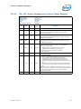
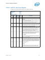
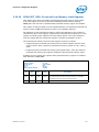
Revision History
§ §
Revision
Number
Description
Revision
Date
001 • Initial release
January
2011
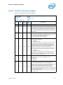
002
•Added Intel
®
Pentium
®
processor family desktop
• Updated DSTS-Device Status Register (B/D/F/Type: 0/1/0/PCI)
• Added four registers to Section 2.13, MCHBAR Registers in Memory
Controller – Channel 0.
• Added four registers to Section 2.14, MCHBAR Registers in Memory
Controller – Channel 1
May 2011
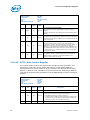
003 • Added Intel
®
Celeron
®
processor family desktop
September
2011

Datasheet, Volume 2 11
Introduction
1 Introduction
This is Volume 2 of the Datasheet for the following products:
• 2nd Generation Intel
®
Core™ processor family desktop
•Intel
®
Pentium
®
processor family desktop
•Intel
®
Celeron
®
processor family desktop
The processor contains one or more PCI devices within a single physical component.
The configuration registers for these devices are mapped as devices residing on the PCI
Bus assigned for the processor socket. This document describes these configuration
space registers or device-specific control and status registers (CSRs) only. This
document does NOT include Model Specific Registers (MSRs).
Note: Throughout this document, the Intel
®
Core™ 17, i5, and i3 desktop processor series,
Intel
®
Pentium
®
processor family desktop, and Intel
®
Celeron
®
processor family
desktop may be referred to as “processor”.
Note: Throughout this document, the Intel
®
6 Series Chipset Platform Controller Hub may
also be referred to as “PCH”.
Note: The term “DT” refers to desktop platforms.
§ §

Introduction
12 Datasheet, Volume 2

Datasheet, Volume 2 13
Processor Configuration Registers
2 Processor Configuration
Registers
This chapter contains the following:
• Register terminology
• PCI Devices and Functions on processor
• System address map
• Processor register introduction
• Detailed register bit descriptions
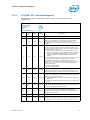
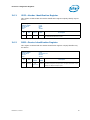
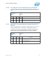
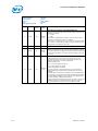
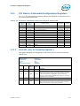
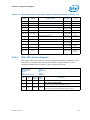
2.1 Register Terminology
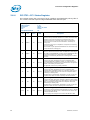
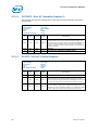
Table 2-1 shows the register-related terminology and register attributes that are used
in this document. Attribute modifiers are listed in Table 2-2.
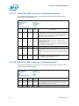
Table 2-1. Register Attributes and Terminology
Item Description
RO
Read Only: These bits can only be read by software, writes have no effect. The value of the
bits is determined by the hardware only.
RW Read / Write: These bits can be read and written by software.
RW1C
Read / Write 1 to Clear: These bits can be read and cleared by software. Writing a '1' to a bit
will clear it, while writing a '0' to a bit has no effect. Hardware sets these bits.
RW0C
Read / Write 0 to Clear: These bits can be read and cleared by software. Writing a ‘0’ to a bit
will clear it, while writing a ‘1’ to a bit has no effect. Hardware sets these bits.
RW1S
Read / Write 1 to Set: These bits can be read and set by software. Writing a ‘1’ to a bit will
set it, while writing a ‘0’ to a bit has no effect. Hardware clears these bits.
RsvdP
Reserved and Preserved: These bits are reserved for future RW implementations and their
value must not be modified by software. When writing to these bits, software must preserve the
value read. When SW updates a register that has RsvdP fields, it must read the register value
first so that the appropriate merge between the RsvdP and updated fields will occur.
RsvdZ
Reserved and Zero: These bits are reserved for future RW1C implementations. SW must use
0 for writes.
WO
Write Only: These bits can only be written by software, reads return zero.
Note: Use of this attribute type is deprecated and can only be used to describe bits without
persistent state.
RC
Read Clear: These bits can only be read by software, but a read causes the bits to be cleared.
Hardware sets these bits.
Note: Use of this attribute type is only allowed on legacy functions, as side-effects on reads are
not desirable.
RSW1C
Read Set / Write 1 to Clear: These bits can be read and cleared by software. Reading a bit
will set the bit to ‘1’. Writing a ‘1’ to a bit will clear it, while writing a ‘0’ to a bit has no effect.
RCW
Read Clear / Write: These bits can be read and written by software, but a read causes the
bits to be cleared.
Note: Use of this attribute type is only allowed on legacy functions, as side-effects on reads are
not desirable.

Processor Configuration Registers
14 Datasheet, Volume 2
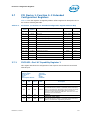
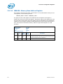
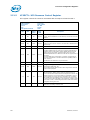
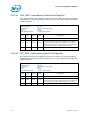
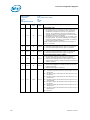
2.2 PCI Devices and Functions on Processor
Note:
1. Not all devices are enabled in all configurations.
2. See Section 2.8.2, “DID2—Device Identification Register” for additional information on graphics DID
values.
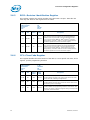
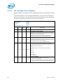
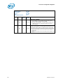
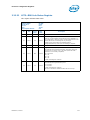
Table 2-2. Register Attribute Modifiers
Attribute
Modifier
Applicable
Attribute
Description
S
RO (w/ -V)
Sticky: These bits are only re-initialized to their default value by a "Power Good
Reset".
Note: Does not apply to RO (constant) bits.
RW
RW1C
RW1S
-K RW
Key: These bits control the ability to write other bits (identified with a 'Lock'
modifier)
-L
RW Lock: Hardware can make these bits "Read Only" via a separate configuration
bit or other logic.
Note: Mutually exclusive with 'Once' modifier.
WO
-O
RW Once: After reset, these bits can only be written by software once, after which
they become "Read Only".
Note: Mutually exclusive with 'Lock' modifier and does not make sense with
'Variant' modifier.
WO
-FW RO
Firmware Write: The value of these bits can be updated by firmware (PCU,
TAP, etc.).
-V
RO Variant: The value of these bits can be updated by hardware.
Note: RW1C and RC bits are variant by definition and therefore do not need
to be modified.
RW
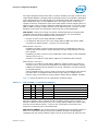
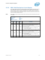
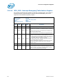
Description DID Device Function
DRAM Controller
0100h
00
PCI Express Controller 0101h 1 0
PCI Express Controller 0105h 1 1
PCI Express Controller 0109h 1 2
Integrated Graphics Device
2
0102h
20
PCI Express Controller 010Dh 6 0

Datasheet, Volume 2 15
Processor Configuration Registers
2.3 System Address Map
The processor supports 512 GB (39 bit) of addressable memory space and 64 KB+3 of
addressable I/O space.
This section focuses on how the memory space is partitioned and what the separate
memory regions are used for. I/O address space has simpler mapping and is explained
near the end of this section.
The processor supports PEG port upper prefetchable base/limit registers. This allows
the PEG unit to claim I/O accesses above 32 bit. Addressing of greater than 4 GB is
allowed on either the DMI Interface or PCI Express interface. The processor supports a
maximum of 32 GB of DRAM. No DRAM memory will be accessible above 32 GB. DRAM
capacity is limited by the number of address pins available. There is no hardware lock
to stop someone from inserting more memory than is addressable.
When running in internal graphics mode, processor initiated Tilex/Tiley/linear
reads/writes to GMADR range are supported. Write accesses to GMADR linear regions
are supported from both DMI and PEG. GMADR write accesses to tileX and tileY regions
(defined using fence registers) are not supported from DMI or the PEG port. GMADR
read accesses are not supported from either DMI or PEG.
In the following sections, it is assumed that all of the compatibility memory ranges
reside on the DMI Interface. The exception to this rule is VGA ranges, which may be
mapped to PCI Express*, DMI, or to the internal graphics device (IGD). In the absence
of more specific references, cycle descriptions referencing PCI should be interpreted as
the DMI Interface/PCI, while cycle descriptions referencing PCI Express or IGD are
related to the PCI Express bus or the internal graphics device respectively. The
processor does not remap APIC or any other memory spaces above TOLUD (Top of Low
Usable DRAM). The TOLUD register is set to the appropriate value by BIOS. The
remapbase/remaplimit registers remap logical accesses bound for addresses above
4 GB onto physical addresses that fall within DRAM.
The Address Map includes a number of programmable ranges:
• Device 0
— PXPEPBAR – PxP egress port registers. (4 KB window)
— MCHBAR – Memory mapped range for internal MCH registers. (32 KB window)
— DMIBAR – This window is used to access registers associated with the
processor/PCH Serial Interconnect (DMI) register memory range. (4 KB
window)
— GGC.GMS – Graphics Mode Select. Used to select the amount of main memory
that is pre-allocated to support the internal graphics device in VGA (non-linear)
and Native (linear) modes. (0–512 MB options).
— GGC.GGMS – GTT Graphics Memory Size. Used to select the amount of main
memory that is pre-allocated to support the Internal Graphics Translation Table.
(0–2 MB options).
For each of the following four device functions
• Device 1, Function 0
• Device 1, Function 1
• Device 1, Function 2

Processor Configuration Registers
16 Datasheet, Volume 2
• Device 6, Function 0
— MBASE/MLIMIT – PCI Express port non-prefetchable memory access window.
— PMBASE/PMLIMIT – PCI Express port prefetchable memory access window.
— PMUBASE/PMULIMIT – PCI Express port upper prefetchable memory access
window
— IOBASE/IOLIMIT – PCI Express port I/O access window.
• Device 2, Function 0
— IOBAR – I/O access window for internal graphics. Through this window
address/data register pair, using I/O semantics, the IGD and internal graphics
instruction port registers can be accessed. Note, this allows accessing the same
registers as GTTMMADR. The IOBAR can be used to issue writes to the
GTTMMADR or the GTT table.
— GMADR – Internal graphics translation window (128 MB, 256 MB, 512 MB
window).
— GTTMMADR – This register requests a 4 MB allocation for combined Graphics
Translation Table Modification Range and Memory Mapped Range. GTTADR will
be at GTTMMADR + 2 MB while the MMIO base address will be the same as
GTTMMADR.
The rules for the above programmable ranges are:
1. For security reasons, the processor will now positively decode (FFE0_0000h to
FFFF_FFFFh) to DMI. This ensures the boot vector and BIOS execute off PCH.
2. ALL of these ranges MUST be unique and NON-OVERLAPPING. It is the BIOS or
system designers' responsibility to limit memory population so that adequate PCI,
PCI Express, High BIOS, PCI Express Memory Mapped space, and APIC memory
space can be allocated.
3. In the case of overlapping ranges with memory, the memory decode will be given
priority. This is a Intel TXT requirement. It is necessary to get Intel TXT protection
checks, avoiding potential attacks.
4. There are NO Hardware Interlocks to prevent problems in the case of overlapping
ranges.
5. Accesses to overlapped ranges may produce indeterminate results.
6. Software must not access B0/D0/F0 32-bit memory-mapped registers with
requests that cross a DW boundary.
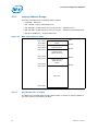
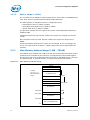
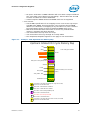
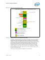
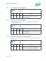
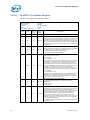
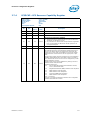
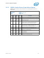
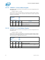
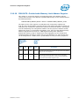
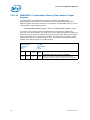
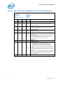
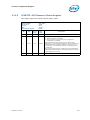
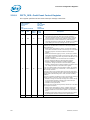
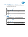
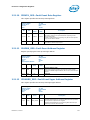
Figure 2-1 represents system memory address map in a simplified form.

Datasheet, Volume 2 17
Processor Configuration Registers
Figure 2-1. System Address Range Example
Main
Memory
Add Range
OS
VISIBLE
< 4 GB
PCI
Memory
Add. Range
(subtractively
decoded to
DMI)
HOST/SYSTEM VIEW
PHYSICAL MEMORY
(DRAM CONTROLLER VIEW)
TSEG
0
0
TSEG BASE
GFX Stolen
(0-256 MB)
ME-UMA
TOM
GFX GTT Stolen BASE
MESEG BASE
1 MB aligned
1 MB aligned
OS invisible
Reclaim
1 MB aligned
for reclaim
1 MB aligned
4 GB
FEC0_0000
1 MB aligned
TOUUD BASE
1 MB aligned
GFX GTT
STOLEN
(0-2 MB)
GFX Stolen BASE
1 MB aligned
TSEG
(0-8 MB)
Legacy
Add. Range
1 MB
Main
memory
Address
Range
OS visible
> 4 GB
Main
Memory
Reclaim
Add Range
Reclaim BASE
Reclaim Limit =
Reclaim Base + x
1 MB aligned
PCI
Memory
Add. Range
(subtractively
decoded to
DMI)
1 MB aligned
512 GB
X
Flash, APIC
Intel TXT
(20 MB)
TOLUD BASE

Processor Configuration Registers
18 Datasheet, Volume 2
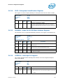
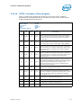
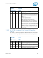
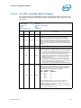
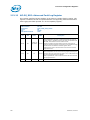
2.3.1 Legacy Address Range
This area is divided into the following address regions:
• 0–640 KB – DOS Area
• 640–768 KB – Legacy Video Buffer Area
• 768–896 KB in 16 KB sections (total of 8 sections) – Expansion Area
• 896–960 KB in 16 KB sections (total of 4 sections) – Extended System BIOS Area
• 960 KB–1 MB Memory – System BIOS Area
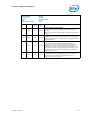
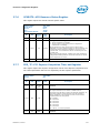
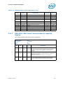
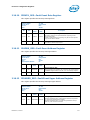
2.3.1.1 DOS Range (0h–9_FFFFh)
The DOS area is 640 KB (0000_0000h–0009_FFFFh) in size and is always mapped to
the main memory controlled by the MCH.
Figure 2-2. DOS Legacy Address Range
Expansion Area
128 KB (16 KB x 8)
000C_0000h
000D_FFFFh
896 KB
Extended System BIOS (Lower)
64 KB (16 KB x 4)
000E_0000h
000E_FFFFh
960 KB
Legacy Video Area
(SMM Memory)
128 KB
000A_0000h
000B_FFFFh
768 KB
DOS Area
0000_0000h
0009_FFFFh
640 KB
System BIOS (Upper)
64 KB
000F_0000h
000F_FFFFh
1 MB

Datasheet, Volume 2 19
Processor Configuration Registers
2.3.1.2 Legacy Video Area (A_0000h–B_FFFFh)
The legacy 128 KB VGA memory range, frame buffer, (000A_0000h–000B_FFFFh) can
be mapped to IGD (Device 2), to PCI Express (Device 1 or Device 6), and/or to the DMI
Interface. The appropriate mapping depends on which devices are enabled and the
programming of the VGA steering bits. Based on the VGA steering bits, priority for VGA
mapping is constant. The processor always decodes internally mapped devices first.
Non-SMM-mode processor accesses to this range are considered to be to the Video
Buffer Area as described above.
The processor always positively decodes internally mapped devices, namely the IGD
and PCI-Express. Subsequent decoding of regions mapped to PCI Express or the DMI
Interface depends on the Legacy VGA configuration bits (VGA Enable and MDAP). This
region is also the default for SMM space.
Compatible SMRAM Address Range (A_0000h–B_FFFFh)
When compatible SMM space is enabled, SMM-mode processor accesses to this range
route to physical system DRAM at 000A_0000h–000B_FFFFh.
PCI Express and DMI originated cycles to enable SMM space are not allowed and are
considered to be to the Video Buffer Area, if IGD is not enabled as the VGA device. DMI
initiated write cycles are attempted as peer write cycles to a VGA enabled PCIe port.
Monochrome Adapter (MDA) Range (B_0000h–B_7FFFh)
Legacy support requires the ability to have a second graphics controller (monochrome)
in the system. Accesses in the standard VGA range are forwarded to IGD, PCI-Express,
or the DMI Interface (depending on configuration bits). Since the monochrome adapter
may be mapped to any of these devices, the processor must decode cycles in the MDA
range (000B_0000h–000B_7FFFh) and forward either to IGD, PCI-Express, or the DMI
Interface. This capability is controlled by the VGA steering bits and the legacy
configuration bit (MDAP bit). In addition to the memory range B0000h to B7FFFh, the
processor decodes I/O cycles at 3B4h, 3B5h, 3B8h, 3B9h, 3BAh, and 3BFh and
forwards them to either IGD, PCI-Express, and/or the DMI Interface.
PEG 16-bit VGA Decode
In the PCI to PCI Bridge Architecture Specification, Revision 1.2 it is required that 16-
bit VGA decode be a feature.
When 16-bit VGA decode is disabled, the decode of VGA I/O addresses is performed on
10 lower bits only, essentially mapping also the aliases of the defined I/O addresses.

Processor Configuration Registers
20 Datasheet, Volume 2
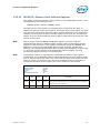
2.3.1.3 PAM (C_0000h–F_FFFFh)
The 13 sections from 768 KB to 1 MB comprise what is also known as the PAM Memory
Area. Each section has Read enable and Write enable attributes.
The PAM registers are mapped in Device 0 configuration space.
• ISA Expansion Area (C_0000h–D_FFFFh)
• Extended System BIOS Area (E_0000h–E_FFFFh)
• System BIOS Area (F_0000h–F_FFFFh)
The processor decodes the Core request, then routes to the appropriate destination
(DRAM or DMI).
Snooped accesses from PCI Express or DMI to this region are snooped on processor
caches.
Non-snooped accesses from PCI Express or DMI to this region are always sent to
DRAM.
Graphics translated requests to this region are not allowed. If such a mapping error
occurs, the request will be routed to C_0000h. Writes will have the byte enables de-
asserted.
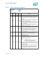
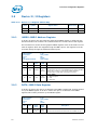
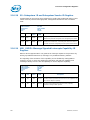
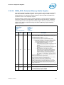
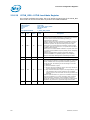
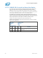
2.3.2 Main Memory Address Range (1 MB – TOLUD)
This address range extends from 1 MB to the top of Low Usable physical memory that is
permitted to be accessible by the processor (as programmed in the TOLUD register).
The processor will route all addresses within this range to the DRAM unless it falls into
the optional TSEG, or optional ISA Hole, or optional IGD stolen VGA memory.
Figure 2-3. Main Memory Address Range
Main Memory
ISA Hole (optional)
DOS Compatibility Memory
0h
FLASH
FFFF_FFFFh
00F0_0000h 15 MB
16 MB
0100_0000h
0 MB
TOLUD
APIC
Main Memory
0010_0000h 1 MB
IGD
Intel TXT
PCI Memory Range
4 GB Max
Contains:
Dev 0, 1, 2, 6, 7
BARS & PCH/PCI
ranges
TSEG
IGGTT
DPR
TSEG_BASE
Page is loading ...
Page is loading ...
Page is loading ...
Page is loading ...
Page is loading ...
Page is loading ...
Page is loading ...
Page is loading ...
Page is loading ...
Page is loading ...
Page is loading ...
Page is loading ...
Page is loading ...
Page is loading ...
Page is loading ...
Page is loading ...
Page is loading ...
Page is loading ...
Page is loading ...
Page is loading ...
Page is loading ...
Page is loading ...
Page is loading ...
Page is loading ...
Page is loading ...
Page is loading ...
Page is loading ...
Page is loading ...
Page is loading ...
Page is loading ...
Page is loading ...
Page is loading ...
Page is loading ...
Page is loading ...
Page is loading ...
Page is loading ...
Page is loading ...
Page is loading ...
Page is loading ...
Page is loading ...
Page is loading ...
Page is loading ...
Page is loading ...
Page is loading ...
Page is loading ...
Page is loading ...
Page is loading ...
Page is loading ...
Page is loading ...
Page is loading ...
Page is loading ...
Page is loading ...
Page is loading ...
Page is loading ...
Page is loading ...
Page is loading ...
Page is loading ...
Page is loading ...
Page is loading ...
Page is loading ...
Page is loading ...
Page is loading ...
Page is loading ...
Page is loading ...
Page is loading ...
Page is loading ...
Page is loading ...
Page is loading ...
Page is loading ...
Page is loading ...
Page is loading ...
Page is loading ...
Page is loading ...
Page is loading ...
Page is loading ...
Page is loading ...
Page is loading ...
Page is loading ...
Page is loading ...
Page is loading ...
Page is loading ...
Page is loading ...
Page is loading ...
Page is loading ...
Page is loading ...
Page is loading ...
Page is loading ...
Page is loading ...
Page is loading ...
Page is loading ...
Page is loading ...
Page is loading ...
Page is loading ...
Page is loading ...
Page is loading ...
Page is loading ...
Page is loading ...
Page is loading ...
Page is loading ...
Page is loading ...
Page is loading ...
Page is loading ...
Page is loading ...
Page is loading ...
Page is loading ...
Page is loading ...
Page is loading ...
Page is loading ...
Page is loading ...
Page is loading ...
Page is loading ...
Page is loading ...
Page is loading ...
Page is loading ...
Page is loading ...
Page is loading ...
Page is loading ...
Page is loading ...
Page is loading ...
Page is loading ...
Page is loading ...
Page is loading ...
Page is loading ...
Page is loading ...
Page is loading ...
Page is loading ...
Page is loading ...
Page is loading ...
Page is loading ...
Page is loading ...
Page is loading ...
Page is loading ...
Page is loading ...
Page is loading ...
Page is loading ...
Page is loading ...
Page is loading ...
Page is loading ...
Page is loading ...
Page is loading ...
Page is loading ...
Page is loading ...
Page is loading ...
Page is loading ...
Page is loading ...
Page is loading ...
Page is loading ...
Page is loading ...
Page is loading ...
Page is loading ...
Page is loading ...
Page is loading ...
Page is loading ...
Page is loading ...
Page is loading ...
Page is loading ...
Page is loading ...
Page is loading ...
Page is loading ...
Page is loading ...
Page is loading ...
Page is loading ...
Page is loading ...
Page is loading ...
Page is loading ...
Page is loading ...
Page is loading ...
Page is loading ...
Page is loading ...
Page is loading ...
Page is loading ...
Page is loading ...
Page is loading ...
Page is loading ...
Page is loading ...
Page is loading ...
Page is loading ...
Page is loading ...
Page is loading ...
Page is loading ...
Page is loading ...
Page is loading ...
Page is loading ...
Page is loading ...
Page is loading ...
Page is loading ...
Page is loading ...
Page is loading ...
Page is loading ...
Page is loading ...
Page is loading ...
Page is loading ...
Page is loading ...
Page is loading ...
Page is loading ...
Page is loading ...
Page is loading ...
Page is loading ...
Page is loading ...
Page is loading ...
Page is loading ...
Page is loading ...
Page is loading ...
Page is loading ...
Page is loading ...
Page is loading ...
Page is loading ...
Page is loading ...
Page is loading ...
Page is loading ...
Page is loading ...
Page is loading ...
Page is loading ...
Page is loading ...
Page is loading ...
Page is loading ...
Page is loading ...
Page is loading ...
Page is loading ...
Page is loading ...
Page is loading ...
Page is loading ...
Page is loading ...
Page is loading ...
Page is loading ...
Page is loading ...
Page is loading ...
Page is loading ...
Page is loading ...
Page is loading ...
Page is loading ...
Page is loading ...
Page is loading ...
Page is loading ...
Page is loading ...
Page is loading ...
Page is loading ...
Page is loading ...
Page is loading ...
Page is loading ...
Page is loading ...
Page is loading ...
Page is loading ...
Page is loading ...
Page is loading ...
Page is loading ...
Page is loading ...
Page is loading ...
Page is loading ...
Page is loading ...
Page is loading ...
Page is loading ...
Page is loading ...
Page is loading ...
Page is loading ...
Page is loading ...
Page is loading ...
Page is loading ...
Page is loading ...
Page is loading ...
Page is loading ...
Page is loading ...
Page is loading ...
Page is loading ...
Page is loading ...
Page is loading ...
Page is loading ...
Page is loading ...
Page is loading ...
Page is loading ...
Page is loading ...
Page is loading ...
Page is loading ...
Page is loading ...
Page is loading ...
Page is loading ...
-
 1
1
-
 2
2
-
 3
3
-
 4
4
-
 5
5
-
 6
6
-
 7
7
-
 8
8
-
 9
9
-
 10
10
-
 11
11
-
 12
12
-
 13
13
-
 14
14
-
 15
15
-
 16
16
-
 17
17
-
 18
18
-
 19
19
-
 20
20
-
 21
21
-
 22
22
-
 23
23
-
 24
24
-
 25
25
-
 26
26
-
 27
27
-
 28
28
-
 29
29
-
 30
30
-
 31
31
-
 32
32
-
 33
33
-
 34
34
-
 35
35
-
 36
36
-
 37
37
-
 38
38
-
 39
39
-
 40
40
-
 41
41
-
 42
42
-
 43
43
-
 44
44
-
 45
45
-
 46
46
-
 47
47
-
 48
48
-
 49
49
-
 50
50
-
 51
51
-
 52
52
-
 53
53
-
 54
54
-
 55
55
-
 56
56
-
 57
57
-
 58
58
-
 59
59
-
 60
60
-
 61
61
-
 62
62
-
 63
63
-
 64
64
-
 65
65
-
 66
66
-
 67
67
-
 68
68
-
 69
69
-
 70
70
-
 71
71
-
 72
72
-
 73
73
-
 74
74
-
 75
75
-
 76
76
-
 77
77
-
 78
78
-
 79
79
-
 80
80
-
 81
81
-
 82
82
-
 83
83
-
 84
84
-
 85
85
-
 86
86
-
 87
87
-
 88
88
-
 89
89
-
 90
90
-
 91
91
-
 92
92
-
 93
93
-
 94
94
-
 95
95
-
 96
96
-
 97
97
-
 98
98
-
 99
99
-
 100
100
-
 101
101
-
 102
102
-
 103
103
-
 104
104
-
 105
105
-
 106
106
-
 107
107
-
 108
108
-
 109
109
-
 110
110
-
 111
111
-
 112
112
-
 113
113
-
 114
114
-
 115
115
-
 116
116
-
 117
117
-
 118
118
-
 119
119
-
 120
120
-
 121
121
-
 122
122
-
 123
123
-
 124
124
-
 125
125
-
 126
126
-
 127
127
-
 128
128
-
 129
129
-
 130
130
-
 131
131
-
 132
132
-
 133
133
-
 134
134
-
 135
135
-
 136
136
-
 137
137
-
 138
138
-
 139
139
-
 140
140
-
 141
141
-
 142
142
-
 143
143
-
 144
144
-
 145
145
-
 146
146
-
 147
147
-
 148
148
-
 149
149
-
 150
150
-
 151
151
-
 152
152
-
 153
153
-
 154
154
-
 155
155
-
 156
156
-
 157
157
-
 158
158
-
 159
159
-
 160
160
-
 161
161
-
 162
162
-
 163
163
-
 164
164
-
 165
165
-
 166
166
-
 167
167
-
 168
168
-
 169
169
-
 170
170
-
 171
171
-
 172
172
-
 173
173
-
 174
174
-
 175
175
-
 176
176
-
 177
177
-
 178
178
-
 179
179
-
 180
180
-
 181
181
-
 182
182
-
 183
183
-
 184
184
-
 185
185
-
 186
186
-
 187
187
-
 188
188
-
 189
189
-
 190
190
-
 191
191
-
 192
192
-
 193
193
-
 194
194
-
 195
195
-
 196
196
-
 197
197
-
 198
198
-
 199
199
-
 200
200
-
 201
201
-
 202
202
-
 203
203
-
 204
204
-
 205
205
-
 206
206
-
 207
207
-
 208
208
-
 209
209
-
 210
210
-
 211
211
-
 212
212
-
 213
213
-
 214
214
-
 215
215
-
 216
216
-
 217
217
-
 218
218
-
 219
219
-
 220
220
-
 221
221
-
 222
222
-
 223
223
-
 224
224
-
 225
225
-
 226
226
-
 227
227
-
 228
228
-
 229
229
-
 230
230
-
 231
231
-
 232
232
-
 233
233
-
 234
234
-
 235
235
-
 236
236
-
 237
237
-
 238
238
-
 239
239
-
 240
240
-
 241
241
-
 242
242
-
 243
243
-
 244
244
-
 245
245
-
 246
246
-
 247
247
-
 248
248
-
 249
249
-
 250
250
-
 251
251
-
 252
252
-
 253
253
-
 254
254
-
 255
255
-
 256
256
-
 257
257
-
 258
258
-
 259
259
-
 260
260
-
 261
261
-
 262
262
-
 263
263
-
 264
264
-
 265
265
-
 266
266
-
 267
267
-
 268
268
-
 269
269
-
 270
270
-
 271
271
-
 272
272
-
 273
273
-
 274
274
-
 275
275
-
 276
276
-
 277
277
-
 278
278
-
 279
279
-
 280
280
-
 281
281
-
 282
282
-
 283
283
-
 284
284
-
 285
285
-
 286
286
-
 287
287
-
 288
288
-
 289
289
-
 290
290
-
 291
291
-
 292
292
-
 293
293
-
 294
294
-
 295
295
-
 296
296


Ask a question and I''ll find the answer in the document
Finding information in a document is now easier with AI
Related papers
-
Intel E3-1220L Datasheet
-
Acer Intel Pentium B940 Datasheet
-
HP AW8063801009607 Datasheet
-
Intel P4X-UPE3210-316-6M1333 Datasheet
-
-
Intel 2760QM Datasheet
-
Intel AV8063801057405 User manual
-
-
-
Other documents
-
Gill OFFSET EXTENSIONS Operating instructions
-
HP Compaq dx7300 Microtower PC Specification
-
HP Compaq dc7100 Convertible Minitower PC User manual
-
HP Compaq dx7200 Slim Tower PC Technical Reference
-
Altera cyclone V User manual
-
Eurotech Adbc8034 Owner's manual
-
kontron FlexATX-KBL-S-C236 User guide
-
-
-
Dolphin SG2010 Reference guide