
22.8.2018 Cmod S7 Reference Manual [Reference.Digilentinc]
https://reference.digilentinc.com/reference/programmable-logic/cmod-s7/reference-manual 1/12
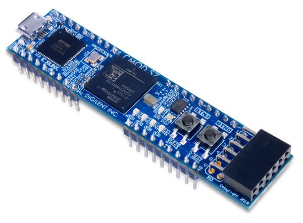
The Digilent Cmod S7 is a small, 48-pin DIP form factor board built around a Xilinx Spartan 7 FPGA. 32 FPGA digital I/O signals, 2
FPGA analog input signals, an external power input rail, and ground are routed to 100-mil-spaced through-hole pins, making the Cmod
S7 well suited for use with solderless breadboards. At just 0.7” by 3.05” inches, it can be loaded in a standard socket and used in
embedded systems. The board also includes a programming ROM (), clock source, USB programming and data transfer circuit, power
supplies, LEDs, and buttons.
(https://reference.digilentinc.com/_media/reference/programmable-logic/cmod-s7/cmod_s7-obl-600.png)
Cmod S7 Reference Manual

22.8.2018 Cmod S7 Reference Manual [Reference.Digilentinc]
https://reference.digilentinc.com/reference/programmable-logic/cmod-s7/reference-manual 2/12
Xilinx Spartan-7 FPGA (XC7S25-1CSGA225C)
Features

22.8.2018 Cmod S7 Reference Manual [Reference.Digilentinc]
https://reference.digilentinc.com/reference/programmable-logic/cmod-s7/reference-manual 3/12
3,650 slices containing four 6-input LUTs and 8 flip-flops
1,620 Kbits of fast block RAM ()
3 clock management tiles, each with a phase-locked loop and mixed-mode clock manager
80 DSP slices
Internal clock speeds exceeding 450 MHz ()
On-chip analog-to-digital converter (XADC)
Programmable over JTAG and Quad-SPI Flash
Memory
4 MB () Quad-SPI Flash
Power
Powered from USB or 5V external supply connected to DIP pin 24
USB
USB-JTAG programming circuitry
USB-UART bridge
Push-buttons and LEDs
2 Buttons
4 LEDs
1 RGB LED ()
Expansion Connectors
1 Pmod connector
8 total FPGA I/O
48-pin DIP form-factor header
32 total FPGA I/O
2 single-ended 0-3.3V analog inputs to XADC
2 power pins
(https://reference.digilentinc.com/_detail/reference/programmable-logic/cmod-s7/cmod-s7-callout.png?id=reference%3Aprogrammable-
logic%3Acmod-s7%3Areference-manual)
Callout Description Callout Description
1 48-pin DIP form factor header 7 UART status LED ()
2 FPGA programming DONE LED () 8 Shared USB JTAG/UART port
3 Pmod connector 9 Power good LED ()
4 User push buttons 10 Spartan-7 FPGA
5 User LEDs 11 SPI Flash
6 User tri-color LED ()
The Cmod S7 is fully compatible with the high-performance Vivado ® Design Suite versions 2018.1 and newer. It is supported under the
free WebPACK™ installation option, which does not require a license, so designs can be implemented at no additional cost. This free
installation includes the ability to create MicroBlaze™ soft-core processor designs. Design resources, example projects, and tutorials are
Software Support

22.8.2018 Cmod S7 Reference Manual [Reference.Digilentinc]
https://reference.digilentinc.com/reference/programmable-logic/cmod-s7/reference-manual 4/12
available for download at the Cmod S7 Resource Center (https://reference.digilentinc.com/reference/programmable-logic/cmod-s7/start).
The Cmod S7 can be used with Vivado 2017.4, but WebPACK installations of this version of Vivado may not contain the device files for
the specific Spartan-7 FPGA used on the Cmod S7. See this Xilinx Answer Record
(https://www.xilinx.com/support/answers/70505.html) for more information, and for a solution.
The Cmod S7 uses a Linear Technologies LTC3569 triple output buck power regulator to generate the needed voltages for the onboard
components. It is connected as shown in Figure 1.1. The characteristics of the outputs are shown in Table 1.1.
(https://reference.digilentinc.com/_detail/reference/programmable-logic/cmod-s7/cmod-s7-power.png?id=reference%3Aprogrammable-
logic%3Acmod-s7%3Areference-manual)
Figure 1.1 Power Supply
Supply Circuits Device
Maximum
Current
3.3V FPGA User I/O, USB Controller, Flash Memory, Pmod Connector, LEDs,
Buttons
IC6:
LTC3569
1.2A
1.8V FPGA, USB Controller IC6:
LTC3569
0.6A
1.0V FPGA Core and Block RAM () IC6:
LTC3569
0.6A
Table 1.1 Power Rail Characteristics
It is possible to power the Cmod S7 from either USB or from an external power supply attached to pins 24 and 25 of the DIP headers,
labeled “VU” and “GND ()”, respectively. The required characteristics of a power source attached to either of these two options is
outlined in Table 1.1.1.
Connector Type Connector Label Min/Rec/Max Voltage
USB J5 Per USB Specification
DIP J3 (Pin 24) 4.5/5.0/5.5
Functional Description
1 Power Supplies
1.1 Power Input Options

22.8.2018 Cmod S7 Reference Manual [Reference.Digilentinc]
https://reference.digilentinc.com/reference/programmable-logic/cmod-s7/reference-manual 5/12
When the Cmod S7 is powered by the USB connector, the voltage from the USB device is driven onto the VU pin. This makes it
possible to power an external circuit from the USB host in addition to the Cmod S7. The VU pin is driven via a schottky diode, so a
small voltage drop will occur, but it should be assumed that the voltage present on VU will be close to 5V.
Warning: When a USB host is attached to the micro USB connector, the VU pin on the DIP headers (pin 24) is driven to the
voltage being provided by the USB host (typically 4.5V-5.5V). To avoid risk of damage, any power source attached to the VU
pin must be disconnected before a USB host is attached. Not taking this precaution can be particularly dangerous if the
power source is a battery.
After power-on, the Spartan-7 FPGA must be configured (or programmed) before it can perform any functions. The FPGA can be
configured in one of two ways:
A PC can use the Digilent USB-JTAG circuitry (port J5) to program the FPGA any time the power is on.
A file stored in the nonvolatile serial (SPI) flash device can be transferred to the FPGA using the SPI port.
Figure 2.1 shows the different options available for configuring the FPGA.
(https://reference.digilentinc.com/_detail/reference/programmable-logic/cmod-s7/cmod-s7-config.png?id=reference%3Aprogrammable-
logic%3Acmod-s7%3Areference-manual)
Figure 2.1 Configuration
The FPGA configuration data is stored in files called bitstreams that have the .bit file extension. The Vivado software from Xilinx can
create bitstreams from VHDL, Verilog®, or block-level designs.
Bitstreams are stored in volatile memory cells within the FPGA. This data defines the FPGA's logic functions and circuit connections,
and it remains valid until it is erased by removing board power, or by writing a new configuration file using the JTAG port.
A Spartan-7 25T bitstream is typically 9,935,224 bits. The time it takes to program the Cmod S7 can be decreased by compressing the
bitstream before programming, and then allowing the FPGA to decompress the bitstream itself during configuration. Depending on
design complexity, compression ratios of 10x can be achieved. Bitstream compression can be enabled within the Xilinx tools to occur
during generation, and is enabled by default in Digilent's master XDC file for the Cmod S7. For more information on how to do this,
consult the Xilinx documentation for the toolset being used.
After successful programming, the FPGA will cause the “DONE” LED () to illuminate.
The following sections provide greater detail about programming the Cmod S7 using the different methods available.
The Xilinx tools typically communicate with FPGAs using the Test Access Port and Boundary-Scan Architecture, commonly referred to
as JTAG. During JTAG programming, a .bit file is transferred from the PC to the FPGA using the onboard Digilent USB-JTAG circuitry
(port J5). JTAG programming can be performed any time after the Cmod S7 has been powered on. If the FPGA is already configured,
then the existing configuration is overwritten with the bitstream being transferred over JTAG.
Programming the Cmod S7 with an uncompressed bitstream using the onboard USB-JTAG circuitry usually takes around
seconds. JTAG programming can be performed by Vivado's Hardware Manager.
Since the FPGA's memory on the Cmod S7 is volatile, it relies on the Quad-SPI flash memory to store the configuration between power
cycles. This configuration mode is called Master SPI. The blank FPGA takes the role of master and reads the configuration file out of the
flash device upon power-up. To that effect, a configuration file needs to first be written to the flash. When programming a non-volatile
flash device, a bitstream file is transferred to the flash in a two-step process. First, the FPGA is programmed with a circuit that can
program flash devices, and then data is transferred to the flash device via the FPGA circuit (this complexity is hidden from the user by
the Xilinx tools). This is called indirect programming. After the flash device has been programmed, it will automatically configure the
FPGA at any subsequent power-on event. Programming files stored in the flash device will remain until they are overwritten, regardless
of power-cycle events.
Quad-SPI programming can be performed using Vivado's Hardware Manager.
2 FPGA Configuration
2.1 JTAG Configuration
2.2 Quad-SPI Configuration

22.8.2018 Cmod S7 Reference Manual [Reference.Digilentinc]
https://reference.digilentinc.com/reference/programmable-logic/cmod-s7/reference-manual 6/12
FPGA Configuration files can be written to the Quad-SPI Flash (Macronix part number MX25L3233F). The FPGA will automatically
read a configuration file from this device at power on. A Spartan-7 25T configuration file requires 9,935,224 bits of memory, leaving
about 69% of the flash device (or ~2.8 MB ()) available for user data. A common use for this extra memory is to store MicroBlaze
programs too big to fit in the onboard block memory. These programs are then loaded and executed using a smaller bootloader program
that can fit in the block memory. It is possible to automatically generate this bootloader, roll it into the bitstream, and then program the
bitstream and large MicroBlaze program into the Quad SPI Flash using Xilinx SDK.
The contents of the memory can be manipulated by issuing certain commands on the SPI bus. The implementation of this protocol is
outside the scope of this document. Xilinx's AXI Quad SPI IP core can be used to read/write the flash in a MicroBlaze design. Refer to
Xilinx's product guide (https://www.xilinx.com/support/documentation/ip_documentation/axi_quad_spi/v3_2/pg153-axi-quad-spi.pdf) for
this core to learn more about using it, or to Macronix's datasheet
(http://www.macronix.com/Lists/Datasheet/Attachments/6744/MX25L3233F,%203V,%2032Mb,%20v1.6.pdf) for the flash device to learn how
to implement a custom controller. All signals in the SPI bus are general-purpose user I/O pins after FPGA configuration and can be
used like any other FPGA I/O.
(https://reference.digilentinc.com/_detail/reference/programmable-logic/cmod-s7/cmod-s7-flash.png?id=reference%3Aprogrammable-
logic%3Acmod-s7%3Areference-manual)
Figure 3.1 Flash Interface
The Cmod S7 includes a 12 MHz () crystal oscillator connected to pin M9 (an MRCC input on bank 14). This clock is intended to be
used as a general purpose system clock. The clock can drive MMCMs to generate clocks of various frequencies and with known phase
relationships that may be needed throughout a design. The 12 MHz () input clock cannot directly drive a PLL because they have a
minimum input frequency of 19 MHz (). Some rules restrict which MMCMs and PLLs may be driven by the 12 MHz () input clock. For a
full description of these rules and of the capabilities of the Spartan-7 clocking resources, refer to Xilinx UG472
(https://www.xilinx.com/support/documentation/user_guides/ug472_7Series_Clocking.pdf), titled “7 Series FPGAs Clocking Resources User
Guide”.
Xilinx offers the Clocking Wizard IP core to help users generate the different clocks required for a specific design. This wizard will
properly instantiate the needed MMCMs and PLLs based on the desired frequencies and phase relationships specified by the user. The
wizard will then output an easy-to-use wrapper component around these clocking resources that can be inserted into the user’s design.
The clocking wizard can be accessed from within the Vivado and IP Integrator tools.
(https://reference.digilentinc.com/_detail/reference/programmable-logic/cmod-s7/cmod-s7-clocking.png?id=reference%3Aprogrammable-
logic%3Acmod-s7%3Areference-manual)
Figure 4.1 Clock Input
3 Quad-SPI Flash
4 Oscillators/Clocks

22.8.2018 Cmod S7 Reference Manual [Reference.Digilentinc]
https://reference.digilentinc.com/reference/programmable-logic/cmod-s7/reference-manual 7/12
The Cmod S7 includes an FTDI FT2232HQ USB-UART bridge (attached to Micro-USB connector J5) that allows the user to use PC
applications to communicate with the board using standard Windows COM port commands. Free USB-COM drivers, available from
FTDI's website (https://www.ftdichip.com) under the “Virtual Com Port” or VCP heading, convert USB packets to UART/serial data.
Serial port data is exchanged with the FPGA using a two-wire serial port (TXD/RXD). After the drivers are installed, I/O commands
can be used from the PC directed to the COM port to produce serial data traffic on the K15 and L12 FPGA pins.
An onboard status LED () (LD6) provides visual feedback on traffic flowing through the port.
The FT2232HQ is also used as the controller for the Digilent USB-JTAG circuitry, but the USB-UART and USB-JTAG functions
behave netirely independant of one another. Programmers interested in using the UART functionality of the FT2232 within their designs
do not need to worry about the JTAG circuitry interfering with the UART data transfers, and vice-versa. The combination of these two
features into a single device allows the Cmod S7 to be programmed, communicated with via UART, and powered from a computer
attached with a single Micro USB cable.
The connections between the FT2232HQ and the Spartan-7 are shown in Figure 5.1. Signal names that imply direction are from the
point-of-view of the DTE (Data Terminal Equipment), in this case, a PC connected to the Micro USB port.
(https://reference.digilentinc.com/_detail/reference/programmable-logic/cmod-s7/cmod-s7-usbuart.png?id=reference%3Aprogrammable-
logic%3Acmod-s7%3Areference-manual)
Figure 5.1 USB-UART Bridge
The Cmod S7 includes one RGB LED (), 4 individual LEDs, and 2 push buttons, as shown in Figure 6.1. The push buttons are
connected to the FPGA via series resistors to prevent damage from inadvertent short circuits (a short circuit could occur if an FPGA pin
assigned to a button was inadvertently defined as an output). The buttons are “momentary” switches that normally generate a low output
when they are at rest, and a high output only when they are pressed.
The four individual high-efficiency LEDs are anode-connected to the FPGA via 330 Ohm resistors, so that they will turn on when a
logic-high voltage is applied to their respective I/O pins. Additional LEDs that are not user-accessible indicate power-on, FPGA
programming status, and USB-UART traffic.
The single RGB LED () has three input signals that drive the cathodes of three smaller internal LEDs: one red, one blue, and one green.
Driving the signal corresponding to one of these colors low will illuminate the internal LED (). The RGB LED () will emit a color
dependent on the combination of internal LEDs that are currently being illuminated. For example, if the red and blue signals are driven
low and green is driven high, the RGB LED () will emit a purple color.
Note: Digilent strongly recommends the use of pulse-width modulation (PWM) when driving the RGB LED (). Driving any of the
signals to a steady logic '0' will result in the LED () being illuminated at an uncomfortably bright level. This can be avoided by ensuring
that none of the RGB signals are driven with more than a 50% duty cycle. Using PWM also greatly expands the potential color palette of
the RGB LED (). Individually adjusting the duty cycle of each each color between 50% and 0% causes the different colors to be
illuminated at different intensities, allowing virtually any color to be displayed.
Figure 6.1 shows how each of the LEDs and push buttons are connected to the Spartan-7.
5 USB-UART Bridge (Serial Port)
6 Basic I/O

22.8.2018 Cmod S7 Reference Manual [Reference.Digilentinc]
https://reference.digilentinc.com/reference/programmable-logic/cmod-s7/reference-manual 8/12
(https://reference.digilentinc.com/_detail/reference/programmable-logic/cmod-s7/cmod-s7-basic-io.png?id=reference%3Aprogrammable-
logic%3Acmod-s7%3Areference-manual)
Figure 6.1 Cmod S7 Basic I/O
The Cmod S7 has a 48-pin DIP form factor connector, implemented as four 9-pin headers for connecting to breadboards and custom
fixtures. The pins have 100 mil spacing, and the entire module is 0.7 inches by 3.05 inches. Headers J1 and J3 are separated by 700 mil
lengthwise along the Cmod, measured from the center of the innermost pins, as are headers J2 and J4. Headers J1 and J2 are separated by
600 mil across the board, as are headers J3 and J4. Of the 48 possible pin locations, 36 are populated on the four headers. Of these, 32
are directly connected to FPGA Digital I/Os, 2 are voltage-divided and connected to FPGA analog inputs, and two are connected to
power pins. The pin and header numbers are shown in Figure 7.1.
7 DIP Header

22.8.2018 Cmod S7 Reference Manual [Reference.Digilentinc]
https://reference.digilentinc.com/reference/programmable-logic/cmod-s7/reference-manual 9/12
(https://reference.digilentinc.com/_detail/reference/programmable-logic/cmod-s7/cmod-s7-dip.png?id=reference%3Aprogrammable-logic%3Acmod-
s7%3Areference-manual)
Figure 7.1 DIP Pin Diagram
VU (pin 24) can be used to power the Cmod S7 when it is not connected to a USB Host. When the device is connected to a USB host,
VU is driven by the 5V rail of the USB connector and can be used to power devices external to the Cmod S7. See the Power Supplies
section for more information.
The pins directly connected to the FPGA can be used as general purpose inputs or outputs. Each of these pins is connected to the
FPGA via a 240 Ohm series resistor. The series resistors prevent short circuits that can occur if a user accidentally drives a signal that is
supposed to be used as an input. The downside to this added protection is that these resistors limit the maximum switching speed of
these signals to 25 MHz (). These pins support input voltages of up to 3.5V.
For more information on the electrical characteristics of these pins, please see Xilinx's Spartan-7 Datasheet
(https://www.xilinx.com/support/documentation/data_sheets/ds189-spartan-7-data-sheet.pdf).
Pins 32 and 33 of the DIP headers are used as analog inputs to the XADC module of the FPGA. The FPGA expects that the inputs
range from 0V-1V, so resistor-divider circuits are used on the Cmod S7 to scale down the input voltage from 3.3V. This circuit is shown
in Figure 7.2.1. This circuit allows the XADC module to accurately measure any voltage between 0V and 3.3V (relative to GND () on pin
25) that is applied to these pins. The analog inputs can tolerate input voltages of up to 5.5V, though any voltage above 3.3V will be read
as 3.3V by the XADC module.
7.1 DIP Digital I/O
7.2 Analog Inputs

22.8.2018 Cmod S7 Reference Manual [Reference.Digilentinc]
https://reference.digilentinc.com/reference/programmable-logic/cmod-s7/reference-manual 10/12
(https://reference.digilentinc.com/_media/cmod_a7/cmoda7_b_analog.png)
Figure 7.2.1 Analog Input Circuit
The XADC core within the Spartan-7 is a dual-channel 12-bit analog-to-digital converter capable of operating at 1 MSPS. Either channel
can be driven by either of the two auxiliary analog inputs to the DIP pins. The XADC core is controlled and accessed from a user design
via the Dynamic Reconfiguration port (DRP). The DRP also provides access to a temperature sensor that is internal to the FPGA. For
more information on using the XADC core, refer to Xilinx UG480
(https://www.xilinx.com/support/documentation/user_guides/ug480_7Series_XADC.pdf), titled “7 Series FPGAs and Zynq-7000 All
Programmable SoC XADC Dual 12-Bit 1 MSPS Analog-to-Digital Converter”. A demo that uses the XADC core is available on the
Cmod S7 Resource Center (https://reference.digilentinc.com/reference/programmable-logic/cmod-s7/start)
Pmod connectors are 2×6, right-angle, 100-mil spaced female connectors that mate with standard 2×6 pin headers. Each 12-pin Pmod
connector provides two 3.3V VCC () signals (pins 6 and 12), two Ground signals (pins 5 and 11), and eight logic signals, as sown in
Figure 8.1. The VCC () and Ground pins can deliver up to 200mA of current, but care must be taken not to exceed any of the power
budgets of the onboard regulator or the external power supply (described in the Power Supplies section).
(https://reference.digilentinc.com/_detail/basys3-pmod_connector.png?id=reference%3Aprogrammable-logic%3Acmod-s7%3Areference-manual)
Figure 8.1 Pmod Diagram
Digilent provides a large collection of Pmod accessory boards that can attach to Pmod expansion connectors to add ready-made
functions like A/D ()'s, D/A ()'s, motor drivers, sensors, and other functions. See www.digilentinc.com (http://www.digilentinc.com) for
more information.
The Cmod S7 has one “standard” type Pmod connector, and the FPGA pin connections for it are described in Table 8.1. Standard Pmod
connectors are connected to the FPGA via 200 Ohm series resistors. The series resistors prevent short circuits that can occur if a user
accidentally drives a signal that is supposed to be used as an input. The downside to this added protection is that these resistors can limit
the maximum switching speed of the data signals.
Pmod JA
Pmod Type Standard
Pin 1 J2
Pin 2 H2
Pin 3 H4
Pin 4 F3
Pin 7 H3
8 Pmod Connector

22.8.2018 Cmod S7 Reference Manual [Reference.Digilentinc]
https://reference.digilentinc.com/reference/programmable-logic/cmod-s7/reference-manual 11/12
Pmod JA
Pin 8 H1
Pin 9 G1
Pin 10 F4
Table 8.1. Cmod S7 Pmod Pinout
cmod-s7 (https://reference.digilentinc.com/tag/cmod-s7?do=showtag&tag=cmod-s7), doc (https://reference.digilentinc.com/tag/doc?
do=showtag&tag=doc)
First Name
Last Name
Email Address
Submit
Subscribe to our Newsletter
Xilinx University
Program
(https://store.digilentinc.com/partners/xilinx-
university-program/)
Technology Partners
(https://store.digilentinc.com/technology-
partners/)
Distributors
(https://store.digilentinc.com/our-
distributors/)
Our Partners
Technical Support
Forum
(https://forum.digilentinc.com)
Reference Wiki
(https://reference.digilentinc.com)
Contact Us
(https://store.digilentinc.com/contact-
us/)
Help
Videos
(https://youtube.com/user/digilentinc)
FAQ
(https://resource.digilentinc.com/verify/faq)
Store Info
(https://store.digilentinc.com/store-
info/)
Customer Info
About Us
(https://store.digilentinc.com/
pageid=26)
Shipping & Returns
(https://store.digilentinc.com/
returns/)
Legal
(https://store.digilentinc.com/
Jobs
(https://store.digilentinc.com/
Internships
(https://store.digilentinc.com/
Company Info
(https://twitter.com/digilentinc)
(https://www.facebook.com/Digilent)
(https://www.youtube.com/user/DigilentInc)
Connect With Us

22.8.2018 Cmod S7 Reference Manual [Reference.Digilentinc]
https://reference.digilentinc.com/reference/programmable-logic/cmod-s7/reference-manual 12/12
(https://instagram.com/digilentinc)
(https://github.com/digilent)
(https://www.reddit.com/r/digilent)
(https://www.linkedin.com/company/1454013)
(https://www.flickr.com/photos/127815101@N07)
-
 1
1
-
 2
2
-
 3
3
-
 4
4
-
 5
5
-
 6
6
-
 7
7
-
 8
8
-
 9
9
-
 10
10
-
 11
11
-
 12
12


Ask a question and I''ll find the answer in the document
Finding information in a document is now easier with AI
Related papers
-
Digilent Arty S7 Reference guide
-
Digilent PmodUSBUART Owner's manual
-
-
-
Digilent PmodSWT User manual
-
-
-
-
-
Digilent PmodAMP2 Reference guide
Other documents
-
Xilinx Arty A7 Reference guide
-
 Xantrex 40 A (XADC-40) User manual
-
Speco AIPS03 User manual
-
-
 AMD XILINX EF-VIVADO-ENTER-FL Operating instructions
-
-
 Xantrex 40 A User manual
-
-
-


