6
dc2459af
DEMO MANUAL DC2459A
EXTERNAL CONNECTIONS
GND: Four ground turrets are provided. These are con-
nected directly to the ground plane and are the common
connection for all supplies and signals.
V+ and V–: Power Supply Turrets. ±12V supply. The ±5V
supplies for the LTC1668 and op amp circuits are derived
from this supply.
3.3V: FPGA Power Rail. Do not connect this turret to a
power supply, it is for monitoring the 3.3V supply on the
connected FPGA board.
50M_CLK: Input Clock. Frequency range is DC to 50MHz.
Logic level should be 3.3V when used with an FPGA board.
The logic level can be up to 5V when used with a digital
pattern generator.
OUT+: Voltage from the noninverting DAC output ampli-
fiers. Assembly options A and C use this connector as
the single-ended output. Assembly option B uses this
connector for the noninverting differential output.
OUT–: Voltage from the inverting DAC output amplifier.
Assembly option B uses this connector for the inverting
differential output.
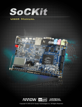
P1: This connector is used to connect to Altera’s SoCkit
board. The pins are 3.3V logic level.
J1: Linduino Connector. Provides a SPI interface to the
FPGA board. The pins are 3.3V logic level.
J2: All pins are ground. These connections are intended
for logic analyzer or digital pattern generator grounds.
J3: This connector is used to connect to the DE0 Nano
FPGA board. The pins are 3.3V to 5V (TTL compatible)
logic level.
J4: This connector is used for the Mimas board and the
Mojo FPGA board. Follow the footprint on the silkscreen
to ensure proper placement. The pins are 3.3V to 5V (TTL
compatible) logic level.
Setting the Frequency of the FPGA Digital Pattern
Generator
The FPGA examples generate a digital sinusoidal output
using either a numerically controlled oscillator (NCO, for
Altera examples) or direct digital synthesizer (DDS, Xilinx
examples). The input to these generators is a 32-bit word
that sets the output frequency according to Equation 1. A
simple SPI interface allows the 32-bit word to be set using
a 4-wire interface from a SPI master such as a Linduino
microcontroller. The MISO output returns the previous
32-bit configuration word, shown in Figure 10.
Equation 1:
CONFIGURE WORD=
SYSTEM CLOCK FREQUENCY • 232 –1
( )
Figure 10. SPI Interface Data Format
CS
PREVIOUS 32-BIT INPUT WORD
32-BIT INPUT WORD
SCK
D31 D30 D29 D28 D27 D26 D25 D24 D23 D22 D21 D20 D19 D18
MSO D17 D16 D15 D14 D13 D12 D11 D10 D9 D8 D7 D6 D5 D4 D3 D2 D1 D0
D31 D30 D29 D28 D27 D26 D25 D24 D23 D22 D21 D20 D19 D18
D17 D16 D15 D14 D13 D12 D11 D10 D9 D8 D7 D6 D5 D4 D3 D2 D1 D0
Downloaded from Arrow.com.Downloaded from Arrow.com.Downloaded from Arrow.com.Downloaded from Arrow.com.Downloaded from Arrow.com.Downloaded from Arrow.com.


