
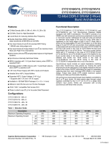
CY7C1166V18, CY7C1177V18
CY7C1168V18, CY7C1170V18
18-Mbit DDR-II+ SRAM 2-Word Burst
Architecture (2.5 Cycle Read Latency)
Cypress Semiconductor Corporation • 198 Champion Court • San Jose, CA 95134-1709 • 408-943-2600
Document Number: 001-06620 Rev. *D Revised March 06, 2008
Features
■ 18 Mbit density (2M x 8, 2M x 9, 1M x 18, 512K x 36)
■ 300 MHz to 400 MHz clock for high bandwidth
■ 2-Word burst for reducing address bus frequency
■ Double Data Rate (DDR) interfaces
(data transferred at 800 MHz) at 400 MHz
■ Read latency of 2.5 clock cycles
■ Two input clocks (K and K) for precise DDR timing
❐ SRAM uses rising edges only
■ Echo clocks (CQ and CQ) simplify data capture in high-speed
systems
■ Data valid pin (QVLD) to indicate valid data on the output
■ Synchronous internally self-timed writes
■ Core V
DD
= 1.8V ± 0.1V; IO V
DDQ
= 1.4V to V
DD
[1]
■ HSTL inputs and Variable drive HSTL output buffers
■ Available in 165-Ball FBGA package (13 x 15 x 1.4 mm)
■ Offered in both Pb-free and non Pb-free packages
■ JTAG 1149.1-compatible test access port
■ Delay Lock Loop (DLL) for accurate data placement
Configurations
With Read Cycle Latency of 2.5 cycles:
CY7C1166V18 – 2M x 8
CY7C1177V18 – 2M x 9
CY7C1168V18 – 1M x 18
CY7C1170V18 – 512K x 36
Functional Description
The CY7C1166V18, CY7C1177V18, CY7C1168V18, and
CY7C1170V18 are 1.8V Synchronous Pipelined SRAMs
equipped with DDR-II+ architecture. The DDR-II+ consists of an
SRAM core with an advanced synchronous peripheral circuitry.
Addresses for read and write are latched on alternate rising
edges of the input (K) clock. Write data is registered on the rising
edges of both K and K
. Read data is driven on the rising edges
of K and K
. Each address location is associated with two 8-bit
words (CY7C1166V18), or 9-bit words (CY7C1177V18), or 18-bit
words (CY7C1168V18), or 36-bit words (CY7C1170V18) that
burst sequentially into or out of the device.
Asynchronous inputs include output impedance matching input
(ZQ). Synchronous data outputs (Q, sharing the same physical
pins as the data inputs D) are tightly matched to the two output
echo clocks CQ/CQ
, eliminating the need for separately
capturing data from each individual DDR SRAM in the system
design.
All synchronous inputs pass through input registers controlled by
the K or K
input clocks. All data outputs pass through output
registers controlled by the K or K
input clocks. Writes are
conducted with on-chip synchronous self-timed write circuitry.
Selection Guide
Description 400 MHz 375 MHz 333 MHz 300 MHz Unit
Maximum Operating Frequency 400 375 333 300 MHz
Maximum Operating Current 1080 1020 920 850 mA
Note
1. The QDR consortium specification for V
DDQ
is 1.5V + 0.1V. The Cypress QDR devices exceed the QDR consortium specification and are capable of supporting
V
DDQ
= 1.4V to V
DD
.
[+] Feedback [+] Feedback

CY7C1166V18, CY7C1177V18
CY7C1168V18, CY7C1170V18
Document Number: 001-06620 Rev. *D Page 2 of 27
Logic Block Diagram (CY7C1166V18)
Logic Block Diagram (CY7C1177V18)
CLK
A
(19:0)
Gen.
K
K
Control
Logic
Address
Register
Read Add. Decode
Read Data Reg.
R/W
DQ
[7:0]
Output
Logic
Reg.
Reg.
Reg.
8
8
16
8
NWS
[1:0]
V
REF
Write Add. Decode
8
8
LD
Control
20
1M x 8 Array
1M x 8 Array
Write
Reg
Write
Reg
CQ
CQ
R/W
DOFF
QVLD
8
CLK
A
(19:0)
Gen.
K
K
Control
Logic
Address
Register
Read Add. Decode
Read Data Reg.
R/W
DQ
[8:0]
Output
Logic
Reg.
Reg.
Reg.
9
9
18
9
BWS
[0]
V
REF
Write Add. Decode
9
9
LD
Control
20
1M x 9 Array
1M x 9 Array
Write
Reg
Write
Reg
CQ
CQ
R/W
DOFF
QVLD
9
[+] Feedback [+] Feedback

CY7C1166V18, CY7C1177V18
CY7C1168V18, CY7C1170V18
Document Number: 001-06620 Rev. *D Page 3 of 27
Logic Block Diagram (CY7C1168V18)
Logic Block Diagram (CY7C1170V18)
CLK
A
(18:0)
Gen.
K
K
Control
Logic
Address
Register
Read Add. Decode
Read Data Reg.
R/W
DQ
[17:0]
Output
Logic
Reg.
Reg.
Reg.
18
18
36
18
BWS
[1:0]
V
REF
Write Add. Decode
18
18
LD
Control
19
512K x 18 Array
512K x 18 Array
Write
Reg
Write
Reg
CQ
CQ
R/W
DOFF
QVLD
18
CLK
A
(17:0)
Gen.
K
K
Control
Logic
Address
Register
Read Add. Decode
Read Data Reg.
R/W
DQ
[35:0]
Output
Logic
Reg.
Reg.
Reg.
36
36
72
36
BWS
[3:0]
V
REF
Write Add. Decode
36
36
LD
Control
18
256K x 36 Array
256K x 36 Array
Write
Reg
Write
Reg
CQ
CQ
R/W
DOFF
QVLD
36
[+] Feedback [+] Feedback

CY7C1166V18, CY7C1177V18
CY7C1168V18, CY7C1170V18
Document Number: 001-06620 Rev. *D Page 4 of 27
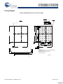
Pin Configurations
CY7C1166V18 (2M x 8)
165-Ball FBGA (13 x 15 x 1.4 mm) Pinout
234 5671
A
B
C
D
E
F
G
H
J
K
L
M
N
P
R
A
CQ
NC
NC
NC
NC
DOFF
NC
NC/72M A
NWS
1
KR/W
NC/144M
NC
NC
NC
NC
NC
TDO
NC
NC
NC
NC
NC
NC
TCK
NC
NC
A NC/288M
K
NWS
0
V
SS
AAA
NC V
SS
V
SS
V
SS
V
SS
V
DD
A
V
SS
V
SS
V
SS
V
DD
DQ4
NC
V
DDQ
NC
NC
NC
NC
DQ7
A
V
DDQ
V
SS
V
DDQ
V
DD
V
DD
DQ5 V
DDQ
V
DD
V
DDQ
V
DD
V
DDQ
V
DD
V
SS
V
DD
V
DDQ
V
DDQ
V
SS
V
SS
V
SS
V
SS
A
A
NC
V
SS
A
A
A
NC V
SS
NC V
SS
NC
NC
V
REF
V
SS
V
DD
V
SS
V
SS
A
V
SS
QVLD
NC
DQ6
NC
NC
NC
V
DD
A
891011
NC
A NC/36M
LD
CQ
A NC
NC
DQ3
V
SS
NC NC NC
NC
V
SS
NC
DQ2
NC
NC
NC
V
REF
NC
NC
V
DDQ
NC
V
DDQ
NC NC
V
DDQ
V
DDQ
V
DDQ
NCV
DDQ
NC
DQ1
NC
V
DDQ
V
DDQ
NC
V
SS
NC NC
NC
TDITMS
V
SS
A
NC
A
NC
NC
NC
ZQ
NC
DQ0
NC
NC
NC
NC
A
CY7C1177V18 (2M x 9)
234 5671
A
B
C
D
E
F
G
H
J
K
L
M
N
P
R
A
CQ
NC
NC
NC
NC
DOFF
NC
NC/72M A NC
K
R/W
NC/144M
NC
NC
NC
NC
NC
TDO
NC
NC
NC
NC
NC
NC
TCK
NC
NC
A NC/288M
K
BWS
0
V
SS
AAA
NC V
SS
V
SS
V
SS
V
SS
V
DD
A
V
SS
V
SS
V
SS
V
DD
DQ4
NC
V
DDQ
NC
NC
NC
NC
DQ7
A
V
DDQ
V
SS
V
DDQ
V
DD
V
DD
DQ5 V
DDQ
V
DD
V
DDQ
V
DD
V
DDQ
V
DD
V
SS
V
DD
V
DDQ
V
DDQ
V
SS
V
SS
V
SS
V
SS
A
A
NC
V
SS
A
A
A
NC V
SS
NC V
SS
NC
NC
V
REF
V
SS
V
DD
V
SS
V
SS
A
V
SS
QVLD
NC
DQ6
NC
NC
NC
V
DD
A
891011
DQ8
A NC/36M
LD
CQ
A NC
NC
DQ3
V
SS
NC NC NC
NC
V
SS
NC
DQ2
NC
NC
NC
V
REF
NC
NC
V
DDQ
NC
V
DDQ
NC NC
V
DDQ
V
DDQ
V
DDQ
NCV
DDQ
NC
DQ1
NC
V
DDQ
V
DDQ
NC
V
SS
NC NC
NC
TDITMS
V
SS
A
NC
A
NC
NC
NC
ZQ
NC
DQ0
NC
NC
NC
NC
A
[+] Feedback [+] Feedback

CY7C1166V18, CY7C1177V18
CY7C1168V18, CY7C1170V18
Document Number: 001-06620 Rev. *D Page 5 of 27
Pin Configurations (continued)
CY7C1168V18 (1M x 18)
165-Ball FBGA (13 x 15 x 1.4 mm) Pinout
234 5671
A
B
C
D
E
F
G
H
J
K
L
M
N
P
R
A
CQ
NC
NC
NC
NC
DOFF
NC
NC/72M A
BWS
1
K
R/W
NC/144M
DQ9
NC
NC
NC
NC
TDO
NC
NC
NC
NC
NC
NC
TCK
NC
NC
A NC/288M
K
BWS
0
V
SS
ANCA
DQ10 V
SS
V
SS
V
SS
V
SS
V
DD
A
V
SS
V
SS
V
SS
V
DD
DQ11
NC
V
DDQ
NC
DQ14
NC
DQ16
DQ17
A
V
DDQ
V
SS
V
DDQ
V
DD
V
DD
DQ13 V
DDQ
V
DD
V
DDQ
V
DD
V
DDQ
V
DD
V
SS
V
DD
V
DDQ
V
DDQ
V
SS
V
SS
V
SS
V
SS
A
A
NC
V
SS
A
A
A
NC V
SS
NC V
SS
DQ12
NC
V
REF
V
SS
V
DD
V
SS
V
SS
A
V
SS
QVLD
NC
DQ15
NC
NC
NC
V
DD
A
891011
DQ0
A NC/36M
LD
CQ
A NC
NC
DQ8
V
SS
NC DQ7 NC
NC
V
SS
NC
DQ6
NC
NC
NC
V
REF
NC
DQ3
V
DDQ
NC
V
DDQ
NC DQ5
V
DDQ
V
DDQ
V
DDQ
NCV
DDQ
NC
DQ4
NC
V
DDQ
V
DDQ
NC
V
SS
NC NC
NC
TDITMS
V
SS
A
NC
A
NC
NC
NC
ZQ
NC
DQ2
NC
DQ1
NC
NC
A
CY7C1170V18 (512K x 36)
234 5671
A
B
C
D
E
F
G
H
J
K
L
M
N
P
R
A
CQ
NC
NC
NC
NC
DOFF
NC
NC/144M NC/36M
BWS
2
K
R/W
BWS
1
DQ27
DQ18
NC
NC
NC
TDO
NC
NC
DQ31
NC
NC
NC
TCK
NC
DQ28
A
BWS
3
K
BWS
0
V
SS
ANCA
DQ19 V
SS
V
SS
V
SS
V
SS
V
DD
A
V
SS
V
SS
V
SS
V
DD
DQ20
DQ21
V
DDQ
DQ32
DQ23
DQ34
DQ25
DQ26
A
V
DDQ
V
SS
V
DDQ
V
DD
V
DD
DQ22 V
DDQ
V
DD
V
DDQ
V
DD
V
DDQ
V
DD
V
SS
V
DD
V
DDQ
V
DDQ
V
SS
V
SS
V
SS
V
SS
A
ANC
V
SS
A
A
A
DQ29 V
SS
NC V
SS
DQ30
NC
V
REF
V
SS
V
DD
V
SS
V
SS
A
V
SS
QVLD
NC
DQ33
NC
DQ35
DQ24
V
DD
A
891011
DQ0
A NC/72M
LD
CQ
A NC
NC
DQ8
V
SS
NC DQ17 DQ7
NC
V
SS
NC
DQ6
DQ14
NC
NC
V
REF
NC
DQ3
V
DDQ
NC
V
DDQ
NC DQ5
V
DDQ
V
DDQ
V
DDQ
DQ4V
DDQ
NC
DQ13
NC
V
DDQ
V
DDQ
NC
V
SS
NC DQ1
NC
TDITMS
V
SS
A
NC
A
DQ16
DQ15
NC
ZQ
DQ12
DQ2
DQ10
DQ11
DQ9
NC
A
[+] Feedback [+] Feedback

CY7C1166V18, CY7C1177V18
CY7C1168V18, CY7C1170V18
Document Number: 001-06620 Rev. *D Page 6 of 27
Pin Definitions
Pin Name IO Pin Description
DQ
[x:0]
Input Output-
Synchronous
Data Input Output Signals. Inputs are sampled on the rising edge of K and K clocks during valid
write operations. These pins drive out the requested data when a read operation is active. Valid data
is driven out on the rising edge of both the K and K clocks during read operations. When read access
is deselected, Q[x:0] are automatically tri-stated.
CY7C1166V18 − DQ
[7:0]
CY7C1177V18 − DQ
[8:0]
CY7C1168V18 − DQ
[17:0]
CY7C1170V18 − DQ
[35:0]
LD Input-
Synchronous
Synchronous Load. This input is brought LOW when a bus cycle sequence is to be defined. This
definition includes address and read/write direction. All transactions operate on a burst of two data.
LD
must meet the setup and hold times around edge of K. LD must meet the setup and hold times
around edge of K.
NWS
0
, NWS
1
, Input-
Synchronous
Nibble Write Select 0, 1 − Active LOW.(CY7C1166V18 Only) Sampled on the rising edge of the K
and K
clocks during write operations. It is used to select the nibble that is written into the device
NWS
0
controls D
[3:0]
and NWS
1
controls D
[7:4]
.
All the Nibble Write Selects are sampled on the same edge as the data. Deselecting a Nibble Write
Select ignores the corresponding nibble of data and not written into the device.
BWS
0
,
BWS
1
,
BWS
2
, BWS
3
Input-
Synchronous
Byte Write Select 0, 1, 2, and 3 − Active LOW. Sampled on the rising edge of the K and K clocks
during Write operations. It is used to select the byte that is written into the device during the current
portion of the write operations. Bytes not written remain unaltered.
CY7C1177V18 − BWS
0
controls D
[8:0]
CY7C1168V18 − BWS
0
controls D
[8:0],
and BWS
1
controls D
[17:9].
CY7C1170V18 − BWS
0
controls D
[8:0]
, BWS
1
controls D
[17:9]
, BWS
2
controls D
[26:18]
, and BWS
3
controls D
[35:27]
.
All the Byte Write Selects are sampled on the same edge as the data. Deselecting a Byte Write Select
ignores the corresponding byte of data and not written into the device.
A Input-
Synchronous
Address Inputs. Sampled on the rising edge of the K clock during active read and write operations.
These address inputs are multiplexed for both read and write operations. Internally, the device is
organized as 2M x 8 (two arrays each of1M x 8) for CY7C1166V18, 2M x 9 (two arrays each of 1M
x 9) for CY7C1177V18, 1M x 18 (two arrays each of 512K x 18) for CY7C1168V18, and 512K x 36
(two arrays each of 256K x 18) for CY7C1170V18. All the address inputs are ignored when the
appropriate port is deselected.
R/W
Input-
Synchronous
Synchronous Read/Write Input. When LD
is LOW, this input designates the access type (read
when R/W
is HIGH, write when R/W is LOW) for loaded address. R/W must meet the setup and hold
times around edge of K.
QVLD Valid Output
Indicator
Valid Output Indicator. The Q Valid indicates valid output data. QVLD is edge aligned with CQ and
CQ
.
K Input-
Clock
Positive Input Clock Input. The rising edge of K is used to capture synchronous inputs to the device
and to drive out data through Q
[x:0]
when in single clock mode. All accesses are initiated on the rising
edge of K.
K
Input-
Clock
Negative Input Clock Input. K is used to capture synchronous inputs being presented to the device
and to drive out data through Q
[x:0]
when in single clock mode.
CQ Clock Output Synchronous Echo Clock Outputs. This is a free running clock and is synchronized to the input
clock (K) of the DDR-II+. The timings for the echo clocks are shown in the “Switching Characteristics”
on page 22.
CQ
Clock Output
Synchronous Echo Clock Outputs. This is a free running clock and is synchronized to the input
clock (K) of the DDR-II+. The timings for the echo clocks are shown in the “Switching Characteristics”
on page 22.
[+] Feedback [+] Feedback

CY7C1166V18, CY7C1177V18
CY7C1168V18, CY7C1170V18
Document Number: 001-06620 Rev. *D Page 7 of 27
ZQ Input Output Impedance Matching Input. This input is used to tune the device outputs to the system data
bus impedance. CQ, CQ, and Q
[x:0]
output impedance are set to 0.2 x RQ, where RQ is a resistor
connected between ZQ and ground. Alternatively, this pin can be connected directly to V
DDQ
, which
enables the minimum impedance mode. This pin cannot be connected directly to GND or left uncon-
nected.
DOFF Input DLL Turn Off − Active LOW. Connecting this pin to ground turns off the DLL inside the device. The
timings in the DLL turned off operation is different from those listed in this data sheet. For normal
operation, this pin can be connected to a pull up through a 10KΩ or less pull up resistor. The device
behaves in DDR-I mode when the DLL is turned off. In this mode, the device can be operated at a
frequency of up to 167 MHz with DDR-I timing.
TDO Output TDO for JTAG.
TCK Input TCK Pin for JTAG.
TDI Input TDI Pin for JTAG.
TMS Input TMS Pin for JTAG.
NC N/A Not Connected to the Die. Tie to any voltage level.
NC/36M N/A Not Connected to the Die. Tie to any voltage level.
NC/72M N/A Not Connected to the Die. Tie to any voltage level.
NC/144M N/A Not Connected to the Die. Tie to any voltage level.
NC/288M N/A Not Connected to the Die. Tie to any voltage level.
V
REF
Input-
Reference
Reference Voltage Input. Static input used to set the reference level for HSTL inputs, outputs, and
AC measurement points.
V
DD
Power Supply Power Supply Inputs to the Core of the Device.
V
SS
Ground Ground for the Device.
V
DDQ
Power Supply Power Supply Inputs for the Outputs of the Device.
Pin Definitions (continued)
Pin Name IO Pin Description
[+] Feedback [+] Feedback

CY7C1166V18, CY7C1177V18
CY7C1168V18, CY7C1170V18
Document Number: 001-06620 Rev. *D Page 8 of 27
Functional Overview
The CY7C1166V18, CY7C1177V18, CY7C1168V18, and
CY7C1170V18 are synchronous pipelined Burst SRAMs
equipped with a DDR interface.
Accesses are initiated on the rising edge of the positive input
clock (K). All synchronous input and output timing are referenced
to the rising edge of the Input clocks (K/K).
All synchronous data inputs (D
[x:0]
) pass through input registers
controlled by the rising edge of the input clocks (K and K
). All
synchronous data outputs (Q
[x:0]
) pass through output registers
controlled by the rising edge of the input clocks (K and K
) also.
All synchronous control (R/W, LD, BWS
[0:X]
) inputs pass through
input registers controlled by the rising edge of the input clock
(K/K).
CY7C1168V18 is described in the following sections. The same
basic descriptions apply to CY7C1166V18, CY7C1177V18, and
CY7C1170V18.
Read Operations
The CY7C1168V18 is organized internally as a single array of
1M x 18. Accesses are completed in a burst of two sequential
18-bit data words. Read operations are initiated by asserting
R/W
HIGH and LD LOW at the rising edge of the positive input
clock (K). The address presented to address inputs is stored in
the read address register. Following the next two K clock rise, the
corresponding 18-bit word of data from this address location is
driven onto the Q
[17:0]
using K as the output timing reference. On
the subsequent rising edge of K the next 18-bit data word from
the address location generated by the burst counter is driven
onto the Q
[17:0]
. The requested data is valid 0.45 ns from the
rising edge of the input clock (K/K
). In order to maintain the
internal logic, each read access must be allowed to complete.
Read accesses can be initiated on every rising edge of the
positive input clock (K).
When read access is deselected, the CY7C1168V18 first
completes the pending read transactions. Synchronous internal
circuitry automatically tri-states the outputs following the next
rising edge of the negative Input clock (K
). This enables for a
seamless transition between devices without the insertion of wait
states in a depth expanded memory.
Write Operations
Write operations are initiated by asserting R/W
LOW and LD
LOW at the rising edge of the positive input clock (K). The
address presented to address inputs is stored in the write
address register. On the following K clock rise the data presented
to D
[17:0]
is latched and stored into the 18-bit Write Data register
provided BWS
[1:0]
are both asserted active. On the subsequent
rising edge of the Negative Input Clock (K
) the information
presented to D
[17:0]
is also stored into the Write Data register
provided BWS
[1:0]
are both asserted active. The 36 bits of data
is then written into the memory array at the specified location.
Write accesses can be initiated on every rising edge of the
positive input clock (K). This pipelines the data flow such that 18
bits of data can be transferred into the device on every rising
edge of the input clocks (K and K
).
When write access is deselected, the device ignores all inputs
after the pending write operations are completed.
Byte Write Operations
Byte Write operations are supported by the CY7C1168V18. A
Write operation is initiated as described in the Write Operations
section. The bytes that are written are determined by BWS
0
and
BWS
1
which are sampled with each set of 18-bit data word.
Asserting the appropriate Byte Write Select input during the data
portion of a write enables the data being presented to be latched
and written into the device. Deasserting the Byte Write Select
input during the data portion of a write enables the data stored in
the device for that byte to remain unaltered. This feature can be
used to simplify read/modify/write operations to a Byte Write
operation.
Double Data Rate Operation
The CY7C1168V18 enables high-performance operation
through high clock frequencies (achieved through pipelining) and
double data rate mode of operation. The CY7C1168V18 requires
two No Operation (NOP) cycle when transitioning from a read to
a write cycle. At higher frequencies, some applications may
require a third NOP cycle to avoid contention.
If a read occurs after a write cycle, then the address and data for
the write are stored in registers. The write information must be
stored because the SRAM cannot perform the last word write to
the array without conflicting with the read. The data stays in this
register until the next write cycle occurs. On the first write cycle
after the read(s), the stored data from the earlier write is written
into the SRAM array. This is called a Posted Write.
If a read is performed on the same address on which a write is
performed in the previous cycle, the SRAM reads out the most
current data. The SRAM does this by bypassing the memory
array and reading the data from the registers.
Depth Expansion
Depth expansion requires replicating the LD control signal for
each bank. All other control signals can be common between
banks as appropriate.
Programmable Impedance
An external resistor, RQ, must be connected between the ZQ pin
on the SRAM and V
SS
to enable the SRAM to adjust its output
driver impedance. The value of RQ must be 5x the value of the
intended line impedance driven by the SRAM. The allowable
range of RQ to guarantee impedance matching with a tolerance
of ±15% is between 175Ω and 350Ω
, with V
DDQ
=1.5V. The
output impedance is adjusted every 1024 cycles upon power up
to account for drifts in supply voltage and temperature.
Echo Clocks
Echo clocks are provided on the DDR-II+ to simplify data capture
on high-speed systems. Two echo clocks are generated by the
DDR-II+. CQ is referenced with respect to K and CQ
is refer-
enced with respect to K
. These are free-running clocks and are
synchronized to the input clock of the DDR-II+. The timings for
the echo clocks are shown in the “Switching Characteristics” on
page 22.
Valid Data Indicator (QVLD)
QVLD is provided on the DDR-II+ to simplify data capture on high
speed systems. The QVLD is generated by the DDR-II+ device
along with data output. This signal is also edge-aligned with the
[+] Feedback [+] Feedback

CY7C1166V18, CY7C1177V18
CY7C1168V18, CY7C1170V18
Document Number: 001-06620 Rev. *D Page 9 of 27
echo clock and follows the timing of any data pin. This signal is
asserted half a cycle before valid data arrives.
DLL
These chips use a Delay Lock Loop (DLL) that is designed to
function between 120 MHz and the specified maximum clock
frequency. The DLL may be disabled by applying ground to the
DOFF
pin. When the DLL is turned off, the device behaves in
DDR-I mode (with 1.0 cycle latency and a longer access time).
For more information, refer to the application note, “DLL Consid-
erations in QDRII/DDRII/QDRII+/DDRII+”. The DLL can also be
reset by slowing or stopping the input clocks K and K for a
minimum of 30 ns. However, it is not necessary for the DLL to be
reset to lock to the desired frequency. During power up, when the
DOFF
is tied HIGH, the DLL gets locked after 2048 cycles of
stable clock.
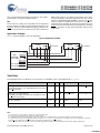
Application Example
Figure 1 shows two DDR-II+ used in an application.
Figure 1. Application Example
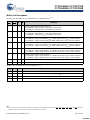
Truth Table
The truth table for the CY7C1166V18, CY7C1177V18, CY7C1168V18, and CY7C1170V18 follows.
[2, 3, 4, 5, 6, 7]
Operation K LD R/W DQ DQ
Write Cycle:
Load address; wait one cycle; input write data on consecutive
K and K
rising edges.
L-H L L D(A) at K (t + 1) ↑ D(A + 1) at K
(t + 1) ↑
Read Cycle: (2.5 Cycle Latency)
Load address; wait two and a half cycle; read data on consec-
utive K and K rising edges.
L-H L H Q(A) at K
(t + 2)↑ Q(A + 1) at K (t + 3) ↑
NOP: No Operation L-H H X High-Z High-Z
Standby: Clock Stopped Stopped X X Previous State Previous State
BUS
MASTER
(CPU or ASIC)
DQ
Addresses
Cycle Start
R/W
Source CLK
Source CLK
Echo Clock1/Echo Clock1
Echo Clock2/Echo Clock2
R = 250ohms
LD R/W
DQ
A
SRAM#1
K
ZQ
CQ/CQ
K
R = 250ohms
LD R/W
DQ
A
SRAM#2
K
ZQ
CQ/CQ
K
Notes
2. X = “Don’t Care,” H = Logic HIGH, L = Logic LOW,
↑ represents rising edge.
3. Device powers up deselected and the outputs in a tri-state condition.
4. “A” represents address location latched by the devices when transaction was initiated and A + 1 represents the addresses sequence in the burst.
5. “t” represents the cycle at which a Read/Write operation is started. t + 1, t + 2, and t + 3 are the first, second, and third clock cycles succeeding the “t” clock cycle.
6. Data inputs are registered at K and K
rising edges. Data outputs are delivered on K and K rising edges.
7. Do K = K
= HIGH when clock is stopped. This is not essential, but permits most rapid restart by overcoming transmission line charging symmetrically.
[+] Feedback [+] Feedback

CY7C1166V18, CY7C1177V18
CY7C1168V18, CY7C1170V18
Document Number: 001-06620 Rev. *D Page 10 of 27
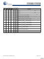
Write Cycle Descriptions
The write cycle descriptions of CY7C1166V18 and CY7C1168V18 follows.
[2, 8]
BWS
0
/
NWS
0
BWS
1
/
NWS
1
K
K
Comments
L L L–H – During the Data portion of a write sequence:
CY7C1166V18 − both nibbles (D
[7:0]
) are written into the device.
CY7C1168V18 − both bytes (D
[17:0]
) are written into the device.
L L – L-H During the Data portion of a write sequence:
CY7C1166V18 − both nibbles (D
[7:0]
) are written into the device.
CY7C1168V18 − both bytes (D
[17:0]
) are written into the device.
L H L–H – During the Data portion of a write sequence:
CY7C1166V18 − only the lower nibble (D
[3:0]
) is written into the device, D
[7:4]
remains unaltered.
CY7C1168V18 − only the lower byte (D
[8:0]
) is written into the device, D
[17:9]
remains unaltered.
L H – L–H During the Data portion of a write sequence:
CY7C1166V18 − only the lower nibble (D
[3:0]
) is written into the device, D
[7:4]
remains unaltered.
CY7C1168V18 − only the lower byte (D
[8:0]
) is written into the device, D
[17:9]
remains unaltered.
H L L–H – During the Data portion of a write sequence:
CY7C1166V18 − only the upper nibble (D
[7:4]
) is written into the device, D
[3:0]
remains unaltered.
CY7C1168V18 − only the upper byte (D
[17:9]
) is written into the device, D
[8:0]
remains unaltered.
H L – L–H During the Data portion of a write sequence:
CY7C1166V18 − only the upper nibble (D
[7:4]
) is written into the device, D
[3:0]
remains unaltered.
CY7C1168V18 − only the upper byte (D
[17:9]
) is written into the device, D
[8:0]
remains unaltered.
H H L–H – No data is written into the devices during this portion of a write operation.
H H – L–H No data is written into the devices during this portion of a write operation.
The write cycle descriptions of CY7C1177V18 follows.
[2, 8]
BWS
0
K K Comments
L L-H – During the Data portion of a Write sequence, the single byte (D
[8:0]
) is written into the device.
L – L-H During the Data portion of a Write sequence, the single byte (D
[8:0]
) is written into the device.
H L-H – No data is written into the device during this portion of a Write operation.
H – L-H No data is written into the device during this portion of a Write operation.
Note
8. Is based on a write cycle was initiated in accordance with the Write Cycle Description Truth Table. Alter NWS
0
, NWS
1
, BWS
0
, BWS
1
, BWS
2
,
and BWS
3
on different
portions of a write cycle, as long as the setup and hold requirements are achieved.
[+] Feedback [+] Feedback

CY7C1166V18, CY7C1177V18
CY7C1168V18, CY7C1170V18
Document Number: 001-06620 Rev. *D Page 11 of 27
The write cycle descriptions of CY7C1170V18 follows.
[2, 8]
BWS
0
BWS
1
BWS
2
BWS
3
K K Comments
LLLLL-H–During the data portion of a write sequence, all four bytes (D
[35:0]
) are written into
the device.
LLLL–L-HDuring the data portion of a write sequence, all four bytes (D
[35:0]
) are written into
the device.
L H H H L-H – During the data portion of a write sequence, only the lower byte (D
[8:0]
) is written
into the device. D
[35:9]
remains unaltered.
L H H H – L-H During the data portion of a write sequence, only the lower byte (D
[8:0]
) is written
into the device. D
[35:9]
remains unaltered.
H L H H L-H – During the data portion of a write sequence, only the byte (D
[17:9]
) is written into
the device. D
[8:0]
and D
[35:18]
remains unaltered.
H L H H – L-H During the data portion of a write sequence, only the byte (D
[17:9]
) is written into
the device. D
[8:0]
and D
[35:18]
remains unaltered.
H H L H L-H – During the data portion of a write sequence, only the byte (D
[26:18]
) is written into
the device. D
[17:0]
and D
[35:27]
remains unaltered.
H H L H – L-H During the data portion of a write sequence, only the byte (D
[26:18]
) is written into
the device. D
[17:0]
and D
[35:27]
remains unaltered.
H H H L L-H – During the data portion of a write sequence, only the byte (D
[35:27]
) is written into
the device. D
[26:0]
remains unaltered.
H H H L – L-H During the data portion of a write sequence, only the byte (D
[35:27]
) is written into
the device. D
[26:0]
remains unaltered.
HHHHL-H–No data is written into the device during this portion of a write operation.
HHHH–L-HNo data is written into the device during this portion of a write operation.
[+] Feedback [+] Feedback

CY7C1166V18, CY7C1177V18
CY7C1168V18, CY7C1170V18
Document Number: 001-06620 Rev. *D Page 12 of 27
IEEE 1149.1 Serial Boundary Scan (JTAG)
These SRAMs incorporate a serial boundary scan test access
port (TAP) in the FBGA package. This part is fully compliant with
IEEE Standard #1149.1-2001. The TAP operates using JEDEC
standard 1.8V IO logic levels.
Disabling the JTAG Feature
It is possible to operate the SRAM without using the JTAG
feature. To disable the TAP controller, TCK must be tied LOW
(V
SS
) to prevent clocking of the device. TDI and TMS are inter-
nally pulled up and may be unconnected. They may alternately
be connected to V
DD
through a pull up resistor. TDO must be left
unconnected. Upon power up, the device comes up in a reset
state which does not interfere with the operation of the device.
Test Access Port—Test Clock
The test clock is used only with the TAP controller. All inputs are
captured on the rising edge of TCK. All outputs are driven from
the falling edge of TCK.
Test Mode Select
The TMS input is used to give commands to the TAP controller
and is sampled on the rising edge of TCK. It is allowable to leave
this pin unconnected if the TAP is not used. The pin is pulled up
internally, resulting in a logic HIGH level.
Test Data-In (TDI)
The TDI pin is used to serially input information into the registers
and connect to the input of any of the registers. The register
between TDI and TDO is chosen by the instruction that is loaded
into the TAP instruction register. For more information about
loading the instruction register, see “TAP Controller State
Diagram” on page 14. TDI is internally pulled up and uncon-
nected if the TAP is not used in an application. TDI is connected
to the most significant bit (MSB) on any register.
Test Data-Out (TDO)
The TDO output pin is used to serially clock data-out from the
registers. The output is active depending upon the current state
of the TAP state machine (see “Instruction Codes” on page 17).
The output changes on the falling edge of TCK. TDO is
connected to the least significant bit (LSb) of any register.
Performing a TAP Reset
A Reset is performed by forcing TMS HIGH (V
DD
) for five rising
edges of TCK. This RESET does not affect the operation of the
SRAM and may be performed while the SRAM is operating. At
power up, the TAP is reset internally to ensure that TDO comes
up in a high-Z state.
TAP Registers
Registers are connected between the TDI and TDO pins and
enable data to be scanned into and out of the SRAM test circuitry.
Select only one register at a time through the instruction
registers. Data is serially loaded into the TDI pin on the rising
edge of TCK. Data is output on the TDO pin on the falling edge
of TCK.
Instruction Register
Load three-bit instructions serially into the instruction register.
This register is loaded when it is placed between the TDI and
TDO pins as shown in “TAP Controller Block Diagram” on
page 15. Upon power up, the instruction register is loaded with
the IDCODE instruction. It is also loaded with the IDCODE
instruction if the controller is placed in a reset state as described
in the previous section.
When the TAP controller is in the Capture IR state, the two least
significant bits are loaded with a binary “01” pattern to allow fault
isolation of the board level serial test path.
Bypass Register
To save time when serially shifting data through registers, it is
sometimes advantageous to skip certain chips. The bypass
register is a single-bit register that can be placed between TDI
and TDO pins. This enables data to be shifted through the SRAM
with minimal delay. The bypass register is set LOW (V
SS
) when
the BYPASS instruction is executed.
Boundary Scan Register
The boundary scan register is connected to all of the input and
output pins on the SRAM. Several no connect (NC) pins are also
included in the scan register to reserve pins for higher density
devices.
The boundary scan register is loaded with the contents of the
RAM Input and Output ring when the TAP controller is in the
Capture-DR state and is then placed between the TDI and TDO
pins when the controller is moved to the Shift-DR state. Use the
EXTEST, SAMPLE/PRELOAD, and SAMPLE Z instructions to
capture the contents of the input and output ring.
The “Boundary Scan Order” on page 18 show the order in which
the bits are connected. Each bit corresponds to one of the bumps
on the SRAM package. The MSb of the register is connected to
TDI, and the LSb is connected to TDO.
Identification (ID) Register
The ID register is loaded with a vendor-specific 32-bit code
during the Capture-DR state when the IDCODE command is
loaded in the instruction register. The IDCODE is hardwired into
the SRAM and can be shifted out when the TAP controller is in
the Shift-DR state. The ID register has a vendor code and other
information described in the “Identification Register Definitions”
on page 17.
TAP Instruction Set
Eight different instructions are possible with the three-bit
instruction register. All combinations are listed in the “Instruction
Codes” on page 17. Three of these instructions are listed as
RESERVED and must not be used. The other five instructions
are described in this section.
Instructions are loaded into the TAP controller during the Shift-IR
state when the instruction register is placed between TDI and
TDO. During this state, instructions are shifted through the
instruction register through the TDI and TDO pins. To execute
the instruction after it is shifted in, the TAP controller must be
moved into the Update-IR state.
[+] Feedback [+] Feedback

CY7C1166V18, CY7C1177V18
CY7C1168V18, CY7C1170V18
Document Number: 001-06620 Rev. *D Page 13 of 27
IDCODE
The IDCODE instruction causes a vendor-specific 32-bit code to
be loaded into the instruction register. It also places the
instruction register between the TDI and TDO pins and enables
the IDCODE to be shifted out of the device when the TAP
controller enters the Shift-DR state. The IDCODE instruction is
loaded into the instruction register upon power up or whenever
the TAP controller is supplied a test logic reset state.
SAMPLE Z
The SAMPLE Z instruction causes the boundary scan register to
be connected between the TDI and TDO pins when the TAP
controller is in a Shift-DR state. The SAMPLE Z command puts
the output bus into a High-Z state until the next command is
supplied during the Update IR state.
SAMPLE/PRELOAD
SAMPLE/PRELOAD is a 1149.1 mandatory instruction. When
the SAMPLE/PRELOAD instructions are loaded into the instruc-
tion register and the TAP controller is in the Capture-DR state, a
snapshot of data on the inputs and output pins is captured in the
boundary scan register.
The user must be aware that the TAP controller clock can only
operate at a frequency up to 20 MHz, while the SRAM clock
operates more than an order of magnitude faster. Because there
is a large difference in the clock frequencies, it is possible that
during the Capture-DR state, an input or output undergoes a
transition. The TAP may then try to capture a signal while in
transition (metastable state). This does not harm the device, but
there is no guarantee as to the value that is captured.
Repeatable results may not be possible.
To guarantee that the boundary scan register captures the cor-
rect value of a signal, the SRAM signal must be stabilized long
enough to meet the TAP controller's capture setup plus hold
times (t
CS
and t
CH
). The SRAM clock input might not be captured
correctly if there is no way in a design to stop (or slow) the clock
during a SAMPLE/PRELOAD instruction. If this is an issue, it is
still possible to capture all other signals and simply ignore the
value of the CK and CK
captured in the boundary scan register.
After the data is captured, it is possible to shift out the data by
putting the TAP into the Shift-DR state. This places the boundary
scan register between the TDI and TDO pins.
PRELOAD enables an initial data pattern to be placed at the
latched parallel outputs of the boundary scan register cells be-
fore the selection of another boundary scan test operation.
The shifting of data for the SAMPLE and PRELOAD phases can
occur concurrently when required—that is, while data captured
is shifted out, the preloaded data can be shifted in.
BYPASS
When the BYPASS instruction is loaded in the instruction register
and the TAP is placed in a Shift-DR state, the bypass register is
placed between the TDI and TDO pins. The advantage of the
BYPASS instruction is that it shortens the boundary scan path
when multiple devices are connected together on a board.
EXTEST
The EXTEST instruction enables the preloaded data to be driven
out through the system output pins. This instruction also selects
the boundary scan register to be connected for serial access
between the TDI and TDO in the shift-DR controller state.
EXTEST Output Bus Tri-State
IEEE Standard 1149.1 mandates that the TAP controller is able
to put the output bus into a tri-state mode.
The boundary scan register has a special bit located at bit #47.
When this scan cell, called the “extest output bus tri-state”, is
latched into the preload register during the Update-DR state in
the TAP controller, it directly controls the state of the output
(Q-bus) pins, when the EXTEST is entered as the current
instruction. When HIGH, it enables the output buffers to drive the
output bus. When LOW, this bit places the output bus into a
High-Z condition.
Set this bit by entering the SAMPLE/PRELOAD or EXTEST
command, and then shifting the desired bit into that cell, during
the Shift-DR state. During Update-DR, the value loaded into that
shift-register cell latches into the preload register. When the
EXTEST instruction is entered, this bit directly controls the output
Q-bus pins. Note that this bit is preset HIGH to enable the output
when the device is powered up, and also when the TAP controller
is in the Test-Logic-Reset state.
Reserved
These instructions are not implemented but are reserved for
future use. Do not use these instructions.
[+] Feedback [+] Feedback

CY7C1166V18, CY7C1177V18
CY7C1168V18, CY7C1170V18
Document Number: 001-06620 Rev. *D Page 14 of 27
TAP Controller State Diagram
Figure 2 shows the tap controller state diagram.
[9]
Figure 2. Tap Controller State Diagram
TEST-LOGIC
RESET
TEST-LOGIC/
IDLE
SELECT
DR-SCAN
CAPTURE-DR
SHIFT-DR
EXIT1-DR
PAUSE-DR
EXIT2-DR
UPDATE-DR
SELECT
IR-SCAN
CAPTURE-IR
SHIFT-IR
EXIT1-IR
PAUSE-IR
EXIT2-IR
UPDATE-IR
1
0
1
1
0
1
0
1
0
0
0
1
1
1
0
1
0
1
0
0
0
1
0
1
1
0
1
0
0
1
1
0
Note
9. The 0/1 next to each state represents the value at TMS at the rising edge of TCK.
[+] Feedback [+] Feedback

CY7C1166V18, CY7C1177V18
CY7C1168V18, CY7C1170V18
Document Number: 001-06620 Rev. *D Page 15 of 27
TAP Controller Block Diagram
Figure 3. Tap Controller Block Diagram
TAP Electrical Characteristics
The Tap Electrical Characteristics table over the operating range follows.
[10, 11, 12]
Parameter Description Test Conditions Min Max Unit
V
OH1
Output HIGH Voltage I
OH
= −2.0 mA 1.4 V
V
OH2
Output HIGH Voltage I
OH
= −100 μA1.6 V
V
OL1
Output LOW Voltage I
OL
= 2.0 mA 0.4 V
V
OL2
Output LOW Voltage I
OL
= 100 μA0.2V
V
IH
Input HIGH Voltage 0.65 V
DD
V
DD
+ 0.3 V
V
IL
Input LOW Voltage –0.3 0.35 V
DD
V
I
X
Input and Output Load Current GND ≤ V
I
≤ V
DD
−55μA
0
012..
29
3031
Boundary Scan Register
Identification Register
012..
.
.106
012
Instruction Register
Bypass Register
Selection
Circuitry
Selection
Circuitry
TAP Controller
TDI
TDO
TCK
TMS
Notes
10.These characteristics pertain to the TAP inputs (TMS, TCK, TDI and TDO). Parallel load levels are specified in the Electrical Characteristics Table.
11. Overshoot: V
IH
(AC) < V
DDQ
+ 0.35V (pulse width less than t
CYC
/2), undershoot: V
IL
(AC) > −0.3V (pulse width less than t
CYC
/2).
12.All voltage refer to ground.
[+] Feedback [+] Feedback

CY7C1166V18, CY7C1177V18
CY7C1168V18, CY7C1170V18
Document Number: 001-06620 Rev. *D Page 16 of 27
TAP AC Switching Characteristics
The Tap AC Switching Characteristics over the operating range follows.
[13, 14]
Parameter Description Min Max Unit
t
TCYC
TCK Clock Cycle Time 50 ns
t
TF
TCK Clock Frequency 20 MHz
t
TH
TCK Clock HIGH 20 ns
t
TL
TCK Clock LOW 20 ns
Setup Times
t
TMSS
TMS Setup to TCK Clock Rise 5 ns
t
TDIS
TDI Setup to TCK Clock Rise 5 ns
t
CS
Capture Setup to TCK Rise 5 ns
Hold Times
t
TMSH
TMS Hold after TCK Clock Rise 5 ns
t
TDIH
TDI Hold after Clock Rise 5 ns
t
CH
Capture Hold after Clock Rise 5 ns
Output Times
t
TDOV
TCK Clock LOW to TDO Valid 10 ns
t
TDOX
TCK Clock LOW to TDO Invalid 0 ns
TAP Timing and Test Condition
The Tap Timing and Test Conditions for the CY7C1166V18, CY7C1177V18, CY7C1168V18, and CY7C1170V18 follows.
[14]
Figure 4. TAP Timing and Test Conditions
t
TL
t
TH
(a)
TDO
C
L
= 20 pF
Z
0
= 50
Ω
GND
0.9V
50
Ω
1.8V
0V
ALL INPUT PULSES
0.9V
Test Clock
Test Mode Select
TCK
TMS
Test Data In
TDI
Test Data Out
t
TCYC
t
TMSH
t
TMSS
t
TDIS
t
TDIH
t
TDOV
t
TDOX
TDO
Notes
13.t
CS
and t
CH
refer to the setup and hold time requirements of latching data from the boundary scan register.
14.Test conditions are specified using the load in TAP AC test conditions. t
R
/t
F
= 1 ns
[+] Feedback [+] Feedback

CY7C1166V18, CY7C1177V18
CY7C1168V18, CY7C1170V18
Document Number: 001-06620 Rev. *D Page 17 of 27
Identification Register Definitions
Instruction Field
Value
Description
CY7C1166V18 CY7C1177V18 CY7C1168V18 CY7C1170V18
Revision Number
(31:29)
000 000 000 000 Version number.
Cypress Device ID
(28:12)
11010111000000101 11010111000001101 11010111000010101 11010111000100101 Defines the type of
SRAM.
Cypress JEDEC ID
(11:1)
00000110100 00000110100 00000110100 00000110100 Allows unique
identification of
SRAM vendor.
ID Register
Presence (0)
1 1 1 1 Indicates the
presence of an ID
register.
Scan Register Sizes
Register Name Bit Size
Instruction 3
Bypass 1
ID 32
Boundary Scan 107
Instruction Codes
Instruction Code Description
EXTEST 000 Captures the input output ring contents.
IDCODE 001 Loads the ID register with the vendor ID code and places the register between TDI
and TDO. This operation does not affect SRAM operation.
SAMPLE Z 010 Captures the Input Output contents. It places the boundary scan register between
TDI and TDO. This forces all SRAM output drivers to a High-Z state.
RESERVED 011 Do Not Use: This instruction is reserved for future use.
SAMPLE/PRELOAD 100 Captures the input output ring contents. It places the boundary scan register between
TDI and TDO. This operation does not affect the SRAM operation.
RESERVED 101 Do Not Use: This instruction is reserved for future use.
RESERVED 110 Do Not Use: This instruction is reserved for future use.
BYPASS 111 Places the bypass register between TDI and TDO. This operation does not affect
SRAM operation.
[+] Feedback [+] Feedback

CY7C1166V18, CY7C1177V18
CY7C1168V18, CY7C1170V18
Document Number: 001-06620 Rev. *D Page 18 of 27
Boundary Scan Order
Bit # Bump ID Bit # Bump ID Bit # Bump ID Bit # Bump ID
0 6R 27 11H 54 7B 81 3G
1 6P 28 10G 55 6B 82 2G
26N 299G 566A 831J
3 7P 30 11F 57 5B 84 2J
4 7N 31 11G 58 5A 85 3K
57R 329F 594A 863J
6 8R 33 10F 60 5C 87 2K
7 8P 34 11E 61 4B 88 1K
8 9R 35 10E 62 3A 89 2L
9 11P 36 10D 63 1H 90 3L
10 10P 37 9E 64 1A 91 1M
11 10N 38 10C 65 2B 92 1L
12 9P 39 11D 66 3B 93 3N
13 10M 40 9C 67 1C 94 3M
1411N 419D 681B 951N
15 9M 42 11B 69 3D 96 2M
16 9N 43 11C 70 3C 97 3P
1711L 449B 711D 982N
18 11M 45 10B 72 2C 99 2P
19 9L 46 11A 73 3E 100 1P
20 10L 47 Internal 74 2D 101 3R
2111K 489A 752E 1024R
22 10K 49 8B 76 1E 103 4P
23 9J 50 7C 77 2F 104 5P
24 9K 51 6C 78 3F 105 5N
25 10J 52 8A 79 1G 106 5R
26 11J 53 7A 80 1F
[+] Feedback [+] Feedback

CY7C1166V18, CY7C1177V18
CY7C1168V18, CY7C1170V18
Document Number: 001-06620 Rev. *D Page 19 of 27
Power Up Sequence in DDR-II+ SRAM
DDR-II+ SRAMs must be powered up and initialized in a
predefined manner to prevent undefined operations. During
power up, when the DOFF is tied HIGH, the DLL gets locked after
2048 cycles of stable clock.
Power Up Sequence
■ Apply power with DOFF tied HIGH (all other inputs can be HIGH
or LOW)
❐ Apply V
DD
before V
DDQ
❐ Apply V
DDQ
before V
REF
or at the same time as V
REF
■ Provide stable power and clock (K, K) for 2048 cycles to lock
the DLL.
DLL Constraints
■ DLL uses K clock as its synchronizing input. The input must
have low phase jitter, which is specified as t
KC Var
.
■ The DLL functions at frequencies down to 120 MHz.
■ If the input clock is unstable and the DLL is enabled, then the
DLL may lock onto an incorrect frequency, causing unstable
SRAM behavior. To avoid this, provide 2048 cycles stable clock
to relock to the desired clock frequency.
Power Up Waveforms
Figure 5. Power Up Waveforms
K
K
Fix HIGH (tie to V
DDQ
)
V
DD
/V
DDQ
DOFF
Clock Start (Clock Starts after V
DD
/V
DDQ
is Stable)
Unstable Clock > 2048 Stable Clock
Start Normal
Operation
~
~
~
~
V
DD
/V
DDQ
Stable (<
+
0.1V DC per 50 ns)
[+] Feedback [+] Feedback

CY7C1166V18, CY7C1177V18
CY7C1168V18, CY7C1170V18
Document Number: 001-06620 Rev. *D Page 20 of 27
Maximum Ratings
Exceeding maximum ratings may shorten the useful life of the
device. User guidelines are not tested.
Storage Temperature ................................ –65°C to + 150°C
Ambient Temperature with Power Applied.–55°C to + 125°C
Supply Voltage on V
DD
Relative to GND.......–0.5V to + 2.9V
Supply Voltage on V
DDQ
Relative to GND..... –0.5V to + V
DD
DC Applied to Outputs in High-Z .........–0.5V to V
DDQ
+ 0.3V
DC Input Voltage
[11]
...............................–0.5V to V
DD
+ 0.3V
Current into Outputs (LOW).........................................20 mA
Static Discharge Voltage (MIL-STD-883, M 3015).... >2001V
Latch up Current..................................................... >200 mA
Operating Range
Range
Ambient
Temperature V
DD
[15]
V
DDQ
[15]
Commercial 0°C to +70°C 1.8 ± 0.1V 1.4V to
V
DD
Industrial –40°C to +85°C
Electrical Characteristic
The DC Electrical Characteristics over the operating range follows.
[12]
Parameter Description Test Conditions Min Typ Max Unit
V
DD
Power Supply Voltage 1.7 1.8 1.9 V
V
DDQ
IO Supply Voltage 1.4 1.5 V
DD
V
V
OH
Output HIGH Voltage Note 16 V
DDQ
/2 – 0.12 V
DDQ
/2 + 0.12 V
V
OL
Output LOW Voltage Note 17 V
DDQ
/2 – 0.12 V
DDQ
/2 + 0.12 V
V
OH(LOW)
Output HIGH Voltage I
OH
= –0.1 mA, Nominal Impedance V
DDQ
– 0.2 V
DDQ
V
V
OL(LOW)
Output LOW Voltage I
OL
= 0.1 mA, Nominal Impedance V
SS
0.2 V
V
IH
Input HIGH Voltage V
REF
+ 0.1 V
DDQ
+ 0.15 V
V
IL
Input LOW Voltage –0.15 V
REF
– 0.1 V
I
X
Input Leakage Current GND ≤ V
I
≤ V
DDQ
–2 2 μA
I
OZ
Output Leakage Current GND ≤ V
I
≤ V
DDQ,
Output Disabled –2 2 μA
V
REF
Input Reference Voltage
[18]
Typical Value = 0.75V 0.68 0.75 0.95 V
I
DD
[19]
V
DD
Operating Supply V
DD
= Max, I
OUT
= 0 mA,
f = f
max
= 1/t
CYC
300 MHz 850 mA
333 MHz 920 mA
375 MHz 1020 mA
400 MHz 1080 mA
I
SB1
Automatic Power Down Current Max V
DD
,
Both Ports Deselected,
V
IN
≥ V
IH
or V
IN
≤ V
IL
f = f
max
= 1/t
CYC
,
Inputs Static
300 MHz 250 mA
333 MHz 260 mA
375 MHz 290 mA
400 MHz 300 mA
AC Input Requirements
Over the operating range
[11]
Parameter Description Test Conditions Min Typ Max Unit
V
IH
Input HIGH Voltage V
REF
+ 0.2 – V
DDQ
+ 0.24 V
V
IL
Input LOW Voltage –0.24 – V
REF
– 0.2 V
Notes
15.Power up: Is based on a linear ramp from 0V to V
DD
(min) within 200 ms. During this time V
IH
< V
DD
and V
DDQ
< V
DD.
16.Outputs are impedance controlled. I
OH
= –(V
DDQ
/2)/(RQ/5) for values of 175Ω < RQ < 350Ω.
17.Outputs are impedance controlled. I
OL
= (V
DDQ
/2)/(RQ/5) for values of 175Ω < RQ < 350Ω
18.V
REF
(min) = 0.68V or 0.46V
DDQ
, whichever is larger, V
REF
(max) = 0.95V or 0.54V
DDQ
, whichever is smaller.
19.The operation current is calculated with 50% read cycle and 50% write cycle.
[+] Feedback [+] Feedback
Page is loading ...
Page is loading ...
Page is loading ...
Page is loading ...
Page is loading ...
Page is loading ...
Page is loading ...
-
 1
1
-
 2
2
-
 3
3
-
 4
4
-
 5
5
-
 6
6
-
 7
7
-
 8
8
-
 9
9
-
 10
10
-
 11
11
-
 12
12
-
 13
13
-
 14
14
-
 15
15
-
 16
16
-
 17
17
-
 18
18
-
 19
19
-
 20
20
-
 21
21
-
 22
22
-
 23
23
-
 24
24
-
 25
25
-
 26
26
-
 27
27


Cypress CY7C1170V18 User manual
- Type
- User manual
- This manual is also suitable for
Ask a question and I''ll find the answer in the document
Finding information in a document is now easier with AI
Related papers
-
 Cypress CY7C1516KV18 User manual
-
 Cypress CY7C1277V18 User manual
-
 Cypress CY7C1916JV18 User manual
-
 Cypress CY7C1992CV18 User manual
-
 Cypress CY7C1516JV18 User manual
-
 Cypress CY7C1316CV18 User manual
-
 Cypress CY7C1568V18 User manual
-
Cypress Computer Hardware 001-07160 User manual
-
 Cypress CY7C1248V18 User manual
-
 Cypress Perform CY7C1513KV18 User manual


