
Baumer Guideline for Switching Outputs V 1.00 EN 1/13 Baumer
27.07.20 Peter Fend (non-confidential) Frauenfeld, Switzerland
Baumer Guideline for Switching Outputs
Scope
This document describes the functionality of switching outputs, such as PNP or NPN. It is intended to provide
support for the correct selection, parameterization and implementation of sensors with binary signals.
The information given must not be understood as a specification and Baumer does not assume any
responsibility for the information provided.
Contents
1 Abstract ......................................................................................................................................... 2
1.1 General information ........................................................................................................................ 2
1.2 Logical states .................................................................................................................................. 2
1.3 Physical implementation ................................................................................................................. 2
1.4 Logical signal assignment .............................................................................................................. 3
1.5 Technological types of switching outputs ....................................................................................... 3
2 Functionality and properties of switching outputs ................................................................... 4
2.1 Transistor outputs ........................................................................................................................... 4
2.1.1 PNP switching output...................................................................................................................... 4
2.1.2 NPN switching output ..................................................................................................................... 4
2.1.3 Push-pull switching output .............................................................................................................. 5
2.2 Relay contacts ................................................................................................................................ 5
2.2.1 Electromagnetic relays ................................................................................................................... 5
2.2.2 Optoelectronic relays ...................................................................................................................... 6
2.3 Operation of switching outputs ....................................................................................................... 7
2.3.1 Current load capacity of switching outputs ..................................................................................... 7
2.3.2 Evaluation of switching signals ....................................................................................................... 7
2.3.3 Fail-safe configuration .................................................................................................................... 8
2.3.4 Antivalent signaling for function monitoring .................................................................................... 8
2.4 Configuration of switching thresholds ............................................................................................. 9
2.4.1 Switching threshold ........................................................................................................................ 9
2.4.2 Switching window ......................................................................................................................... 10
2.5 Extended information transmission with binary signals ................................................................ 11
2.5.1 IO-Link .......................................................................................................................................... 11
2.5.2 Pulse width modulation (PWM) .................................................................................................... 12
2.5.3 Pulse output for summation .......................................................................................................... 12
2.5.4 Frequency output for measured value transmission .................................................................... 12
3 Appendix ..................................................................................................................................... 13
3.1 List of figures ................................................................................................................................ 13
3.2 Documentation history .................................................................................................................. 13

Baumer Guideline for Switching Outputs V 1.00 EN 2/13 Baumer
27.07.20 Peter Fend (non-confidential) Frauenfeld, Switzerland
1 Abstract
1.1 General information
Sensors with switching outputs or binary signals are primarily known for point level detection, as pressure
switches, flow monitors or thermostats. However, continuously measuring sensors can also include switching
outputs to provide additional information or to take over control tasks. In a broader sense, binary signals can
also output information in the form of frequency, pulse width modulation (PWM), pulse summation for flow
rates, etc. IO-Link, which is based on a switching output, can transmit information in both directions in
various operating modes. The guide is therefore not limited to purely binary measuring sensors, but also
deals with the topic of physical interfaces that can only assume binary logic states, e.g. 0 V and 24 V or "0"
or "1".
1.2 Logical states
A distinction is made between two logical states:
inactive Normal condition, e.g. no medium detected, pressure ok or no error
Active Triggered or critical condition, e.g. medium detected, pressure too high or alarm
The exact definition is important for further logical signal processing. It may well be that the state "Medium
detected" is a normal state, e.g. if it is a dry run protection for pumps. Therefore it is recommended to always
use the definitions of the sensor, e.g. in the example "active" with medium detected.
1.3 Physical implementation
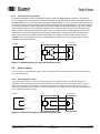
There are basically four different physical versions of switching outputs:
PNP Switch to positive voltage supply potential (+Vs):
NPN Switch to reference potential (GND, 0 V)
Push-pull Switch between positive voltage supply potential (+Vs) and reference potential
(GND, 0 V)
Contact Potential-free switching contact
GND (0 V)
+Vs
Q
GND (0 V)
+Vs
Q
GND (0 V)
+Vs
Q
PNP NPN
R11
R12
GND (0 V)
+Vs
ContactPush-pull
Figure 1: Physical implementation of switching outputs

Baumer Guideline for Switching Outputs V 1.00 EN 3/13 Baumer
27.07.20 Peter Fend (non-confidential) Frauenfeld, Switzerland
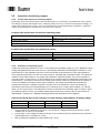
1.4 Logical signal assignment
With binary switching states one speaks of two different logical signal assignments:
Normally Open (NO) Switch in normal (inactive) state open
Normally Closed (NC) Switch closed in normal (inactive) state
GND (0 V)
+Vs
Q
GND (0 V)
+Vs
Q
GND (0 V)
+Vs
Q
PNP NPN
Normally Closed (NC)
GND (0 V)
+Vs
Q
GND (0 V)
+Vs
Q
GND (0 V)
+Vs
Q
PNP NPN
R11
R12
GND (0 V)
+Vs
Normally Open (NO)
R11
R12
GND (0 V)
+Vs
ContactPush-pull
Push-pull Contact
Figure 2: Logical signal assignments for the respective physical implementation
The two variants are generated by the sensor by a simple inversion of the two possible logical states
"inactive" or "active". The correct configuration depends on the desired "fail-safe" state. Normally Closed" is
preferred for an overfill protection, as a defect or broken wire signals the "overfill" state, i.e. the critical state
(see section Fehler! Verweisquelle konnte nicht gefunden werden.).
1.5 Technological types of switching outputs
There are numerous technologies to realize switching outputs. Besides classical electromechanical relays,
integrated circuits are also available. In principle, however, all types can be divided into these categories:
Transistor Potential-bound bipolar or field effect transistor(s)
Relay contact Potential-free switching contact of a
Electromechanical relays
Optoelectronic relay (on semiconductor basis)
Transistors usually switch through the operating voltage potential +Vs or the reference potential GND (0 V)
of the sensor. Any potential can be switched with potential-free relay contacts.

Baumer Guideline for Switching Outputs V 1.00 EN 4/13 Baumer
27.07.20 Peter Fend (non-confidential) Frauenfeld, Switzerland
2 Functionality and properties of switching outputs
2.1 Transistor outputs
Transistor outputs can be built up with discrete components or can be completely or partially in integrated
circuits. Depending on the technology, the switching elements are bipolar or field effect transistors. The
designations PNP and NPN are derived from the bipolar transistors, which is why only these are shown in
the schematic diagrams below.
2.1.1 PNP switching output
The PNP switching output uses a transistor whose emitter or source terminal is connected to the positive
operating voltage potential +Vs. The electronics of the sensor controls this transistor at the base or gate with
a control voltage which is pulled in the direction of the reference potential GND (0 V) when the output is to be
activated. In this case, the collector or drain terminal of the transistor is conductively connected to the
operating voltage potential +Vs. Current then flows from the switching output Q into the load resistor R
L
of
the input in the control device. For an inactive output, the control voltage at the transistor is practically
connected to +Vs, whereupon the transistor blocks and thus no more current can flow out.
GND (0 V)
+Vs
Q
GND (0 V)
+Vs
Q
PNP
R
L
+Vs
Sensor Control equipmentPNP
Figure 3: Schematic diagram of a PNP switching output
2.1.2 NPN switching output
With the NPN switching output, the emitter or source terminal of the transistor is connected to the reference
potential GND (0 V). The control voltage of the sensor electronics connected to the base or gate of the
transistor moves towards the operating voltage potential +Vs for an active output. With such an active output,
the collector or drain connection of the transistor is conductively connected to the reference potential GND
(0 V). Current then flows into the switching output Q from the load resistor R
L
of the input of the control
device. When the output is inactive, the control voltage is practically applied to GND (0 V) so that the
transistor blocks and no more current flow is possible.
GND (0 V)
+Vs
Q
GND (0 V)
+Vs
Q
NPN
R
L
Sensor Control equipmentNPN
+Vs
Figure 4: Schematic diagram of a NPN switching output

Baumer Guideline for Switching Outputs V 1.00 EN 5/13 Baumer
27.07.20 Peter Fend (non-confidential) Frauenfeld, Switzerland
2.1.3 Push-pull switching output
The push-pull switching output is basically a mixture of PNP and NPN switching output. It is controlled in
such a way that only one transistor is conductive at a time, so that the output is either connected to reference
potential GND (0 V) or, in the active state, to voltage supply potential +Vs. The connected control device can
contain any number of load resistors R
L
, the switching potentials are set independently of their size or wiring.
The push-pull switching output is generally found in fast interfaces for data transmission, e.g. with IO-Link in
communication mode. The connected lines always have a capacitance and act as an RC element with the
load resistor R
L
. The respective switching edge, which in the case of PNP or NPN switching output is only
reloaded by R
L
, would be slowed down more and more with higher-resistance R
L
and increasing cable
length, which reduces the maximum data transmission rate. With push-pull switching outputs, the line
capacitances can be reloaded very quickly at both switching edges, since the transistors have very low
resistance in the switched state.
GND (0 V)
+Vs
Q
Push-pull
GND (0 V)
+Vs
Q
NPN
RL
Sensor Control equipment
PNP
R
L
+Vs
Figure 5: Schematic diagram of a push-pull switching output
2.2 Relay contacts
A relay contact is a potential-free switch. This can be mechanical (electromagnetic relay) or optoelectronic
(e.g. Opto-MOS-FET).
2.2.1 Electromagnetic relays
In electromagnetic relays, a current carrying coil moves an armature which actuates the mechanical
switching contact via the magnetic field which builds up. In the inactive state (currentless coil) a spring
returns the armature and the switch contact opens. The logic can also be inverted, the contact is then
opened by energizing the coil. There are also combinations of normally open and normally closed contacts,
the so-called changeover contact.
GND (0 V)
+Vs
R11
Sensor Control equipment
R11
R12
GND (0 V)
+Vs
Contact
R12
+Vs
Figure 6: Principle circuit diagram of an electromagnetic relay

Baumer Guideline for Switching Outputs V 1.00 EN 6/13 Baumer
27.07.20 Peter Fend (non-confidential) Frauenfeld, Switzerland
Due to their size and the relatively high current requirement to supply the coil, electromagnetic relays are
rarely found in sensors. However, they are advantageously used in intrinsically safe isolators (switching
repeaters) for hazardous areas.
NC
0V
+Vs
NO
CleverLevel with PNP
output
+Vs
0V
DI
Control equipment
Hazardous area Safe area
2 NC
L
A
C
B N
Ex i switching repeater
1 COM
3 NO
Figure 7: Example of an intrinsically safe Ex i isolator with electromagnetic relay
2.2.2 Optoelectronic relays
Semiconductor circuits offer the advantages of no moving components and are therefore wear-free. Normal
optocouplers with simple transistors can only switch the current in one direction. This would not be
satisfactory for emulating a contact. Integrated circuits with Opto-MOS-FETs are available which are
internally designed to switch the current in both directions. Such a potential-free contact behaves practically
like an electromechanical relay, provided that the maximum current load capacity is not exceeded.
GND (0 V)
+Vs
R11
Sensor Control equipment
R11
R12
GND (0 V)
+Vs
Contact
R12
+Vs
Figure 8: Principle circuit diagram of an optoelectronic relay
The compact design of semiconductor circuits also allows integration into smaller sensors. Figure 9 shows
an example of a sensor with display, which additionally visualizes the switching states of the two relay
contacts. The terminals Rxx are located on the rear of the electronics insert.
Figure 9: Example of sensor electronics with two optoelectronic relay contacts

Baumer Guideline for Switching Outputs V 1.00 EN 7/13 Baumer
27.07.20 Peter Fend (non-confidential) Frauenfeld, Switzerland
2.3 Operation of switching outputs
2.3.1 Current load capacity of switching outputs
Regardless of the technological type of the switching output, e.g. transistors or potential-free relay contacts,
the switching capacity with regard to max. switching voltage and max. current load is limited accordingly. For
outputs with semiconductor circuits, short-circuit protection is usually implemented. Otherwise, a switching
output can be damaged or destroyed by a short circuit or overload.
Example of the specification of a transistor switching output:
Voltage drop
PNP: (+Vs -0,5 V) ± 0,2 V, Rload ≤ 10 kΩ
NPN: (+0,4 V) ± 0,2 V, Rload ≤ 10 kΩ
Current load capacity
100 mA , max.
Leakage current
< 100 μA
Short-circuit protection
Yes
Example of the specification of a potential-free contact:
On resistance
< 10 Ω
Current load capacity
75 mA , max.
Switching voltage
60 V , max.
Short-circuit protection
Yes
2.3.2 Evaluation of switching signals
Usually the signal swing between "0" and "1" is as large as the operating voltage, e.g. 24 V. Despite the large
voltage swing between the two levels, there is a risk of being affected by electromagnetic interference. The
load resistor R
L
in the evaluation unit of the control unit should not be selected to be too high-impedance,
since capacitive interference currents can easily couple in, especially with unshielded cables. The higher the
resistance of the load resistor R
L
, the greater the interference voltage that arises, since such interference
currents act like a current source, i.e. the magnitude of the coupled current is independent of the load by the
load resistor R
L
. According to Ohm's law, the voltage drop across a resistor is proportional to the product of
current and resistance; therefore, with a higher resistance, the voltage drop and thus the interference
potential also increases. Leakage currents are a further source of interference. These can already be
generated by the sensor (see its specification) or be caused by poor or faulty cable insulation. As a thumb
value one can say that up to 1 mA interference current can flow when the switching output is inactive. When
the switching output is active, you should therefore draw at least 2 mA current to have a clear reserve for
differentiation. Furthermore, a suitable switching threshold with hysteresis must be defined.
Field-proven specification for the evaluation of a PNP switching output with 24 V operating voltage:
Logical state
Voltage (V)
Current (mA)
Load resistance R
L
0
< 5
< 1
< 5 kΩ
1
> 15
> 2 (max. 30)
(< 7,5 kΩ)
At logic state "0" an interference current of 1 mA can flow, the voltage should not exceed 5 V; a load
resistance R
L
of max. 5 kΩ is possible.
In logic state "1" the voltage provided can drop to 15 V, but still at least 2 mA should flow; the maximum
load resistance R
L
is calculated to 7.5 kΩ.
Both conditions are fulfilled by a load resistance R
L
< 5 kΩ.

Baumer Guideline for Switching Outputs V 1.00 EN 8/13 Baumer
27.07.20 Peter Fend (non-confidential) Frauenfeld, Switzerland
The switching threshold is best set in the middle of the voltage limits, i.e. at 10 V; the hysteresis should be at
least 1 V.
The results can be transferred accordingly to an NPN switching output.
2.3.3 Fail-safe configuration
To ensure fail-safe operation, the signaling must behave in such a way that a safe operating state is
established in the event of a fault.
Example: If an overfill protection system with a level switch fails, the switching signal must indicate the state
"Overfill". This switches off the pump or the valve for filling the tank and an alarm can be triggered.
Causes of failure can be:
Voltage supply failure
Line break
Defect of the sensor
If the sensor is defective, it must output a predefined signal. For some sensors, a default can be made in the
parameters for this case.
Example based on an overfill protection compared to a dry run protection:
Application
Medium
detected
PNP/NPN
Relay contact
Normally Open
(NO)
Normally Closed
(NC)
Normally Open
(NO)
Normally Closed
(NC)
Overfill
protection
No
Active
Closed
Yes
Inactive
Open
Dry run
detection
No
Inactive
Open
Yes
Active
Closed
In case of a failure of the voltage supply or a wire break, a PNP or NPN switching output becomes inactive
and a relay contact opens. These states must be selected for signaling the respective critical case. For the
example above this means:
Overfill protection: Normally Closed (NC), switch closed in normal (inactive) state
Dry run protection: Normally Open (NO), switch in normal (inactive) state open
I.e. in case of overfill protection, the switching output must open when a medium is detected, but in case of
dry run protection, the switching output must also open when no medium is detected (red text markings in
above table).
2.3.4 Antivalent signaling for function monitoring
For continuous function monitoring, two switching signals can be transmitted in parallel whose logical values
are inverted (anti-valence). If the signals are no longer inverted when they are evaluated, an error has
occurred.

Baumer Guideline for Switching Outputs V 1.00 EN 9/13 Baumer
27.07.20 Peter Fend (non-confidential) Frauenfeld, Switzerland
NC
0V
+Vs
NO
Switching sensor with
antivalent PNP outputs
+Vs
0V
DI1
Control equipment
DI2
Figure 10: Antivalent signaling for function monitoring using the example of PNP outputs
Truth table for the antivalent signaling:
Sensor status
Inactive
Active
Inactive or active
Output NO
0
1
0
1
Output NC
1
0
0
1
Status
OK
OK
Error
Error
The antivalent signaling can also be realized with the NPN or push-pull versions.
2.4 Configuration of switching thresholds
Continuously measuring sensors with switching output, e.g. pressure switches, have parameters to configure
the switching thresholds or switching windows. The functionality and parameter structure is sensor-specific,
therefore the operating instructions should be consulted to make the appropriate settings.
In the following, the possibilities are explained on a generic basis.
2.4.1 Switching threshold
The parameters for a switching threshold are threshold value and hysteresis. The output signal changes to
the active state when the threshold value is exceeded. Resetting to the inactive state only occurs when the
value falls below the switching threshold minus a so-called hysteresis. This prevents the output signal from
oscillating when the excitation moves close to the switching threshold (see Figure 11).

Baumer Guideline for Switching Outputs V 1.00 EN 10/13 Baumer
27.07.20 Peter Fend (non-confidential) Frauenfeld, Switzerland
Figure 11: Definition of the switching threshold with hysteresis
The definition of the hysteresis is either implemented with a separate parameter or with an absolute reset
threshold value. Such a reset must be performed manually when the threshold value changes.
Furthermore, there are definitions of positive and negative or left and right or centered hysteresis. How the
threshold values generated in this way are implemented can be found in the respective operating
instructions.
2.4.2 Switching window
With the switching window, the output signal is active as long as the excitation is within the two parameters
switching window min. and switching window max. (Figure 12).
Also here there is a hysteresis which is either fixed or parameterizable. In addition to an explicit selection
option between switching threshold and switching window, there is also an implementation which selects the
switching window function if the reset threshold value is greater than the threshold value.
0
10
20
30
40
50
60
70
80
90
100
Modulation of measuring span (%)
Time
Excitation Output signal Threshold
Threshold - hysteresis Hysteresis

Baumer Guideline for Switching Outputs V 1.00 EN 11/13 Baumer
27.07.20 Peter Fend (non-confidential) Frauenfeld, Switzerland
Figure 12: Definition of the switching window
2.5 Extended information transmission with binary signals
2.5.1 IO-Link
IO-Link is based on a switching output. In addition to the standard signaling with a switching output signal, a
corresponding IO-Link master can set the sensor to communication mode. The then bidirectional data
exchange that is possible is based on a digital protocol with a fixed bit rate. In this communication mode, the
output operates in push-pull mode in order not to scramble both signal edges, rising and falling. This results
in a low impedance control which allows a fast reloading of the cable capacities.
C/DI
+Vs
0V
Control equipmentIO-Link sensor
GND (0 V)
+Vs
C/Q
Figure 13: Block diagram of an IO-Link implementation
0
10
20
30
40
50
60
70
80
90
100
Modulation of measuring span (%)
Time
Excitation Output signal Switching window min. Switching window max.

Baumer Guideline for Switching Outputs V 1.00 EN 12/13 Baumer
27.07.20 Peter Fend (non-confidential) Frauenfeld, Switzerland
2.5.2 Pulse width modulation (PWM)
With PWM, a continuous measured value can be transmitted via a binary switching output. The information is
contained in a periodic square-wave signal whose ratio of the duty cycle to the total period length represents
the measured value between 0 and 100 %.
Figure 14: Example for pulse width modulation (PWM)
2.5.3 Pulse output for summation
Flowmeters usually also have a pulse output implemented. When a specified cumulative flow rate is
reached, a pulse is emitted via this output, which is summed up by the evaluation unit. This sum then
corresponds to the total flow rate (volume) over the period under consideration.
Figure 15: Example of a flow meter with display of the cumulated flow rate
2.5.4 Frequency output for measured value transmission
Continuous measured values can be transmitted via a binary signal with variable frequency. The measured
value range 0 ... 100 % is then defined between a lower and upper frequency. Mechanical flowmeters
(turbines), for example, output the flow rate this way. Electronic flow meters (e.g. EMF) emulate this signal to
enable direct replacement.

Baumer Guideline for Switching Outputs V 1.00 EN 13/13 Baumer
27.07.20 Peter Fend (non-confidential) Frauenfeld, Switzerland
3 Appendix
3.1 List of figures
Figure 1: Physical implementation of switching outputs ..................................................................................... 2
Figure 2: Logical signal assignments for the respective physical implementation ............................................. 3
Figure 3: Schematic diagram of a PNP switching output ................................................................................... 4
Figure 4: Schematic diagram of a NPN switching output ................................................................................... 4
Figure 5: Schematic diagram of a push-pull switching output ............................................................................ 5
Figure 6: Principle circuit diagram of an electromagnetic relay .......................................................................... 5
Figure 7: Example of an intrinsically safe Ex i isolator with electromagnetic relay ............................................ 6
Figure 8: Principle circuit diagram of an optoelectronic relay ............................................................................. 6
Figure 9: Example of sensor electronics with two optoelectronic relay contacts ............................................... 6
Figure 10: Antivalent signaling for function monitoring using the example of PNP outputs ............................... 9
Figure 11: Definition of the switching threshold with hysteresis ....................................................................... 10
Figure 12: Definition of the switching window .................................................................................................. 11
Figure 13: Block diagram of an IO-Link implementation .................................................................................. 11
Figure 14: Example for pulse width modulation (PWM) ................................................................................... 12
Figure 15: Example of a flow meter with display of the cumulated flow rate ................................................... 12
3.2 Documentation history
Version
Date
Reviewed by
Amendment / Supplement / Description
V1.00
27.07.2020
fep
Translation from German document V1.00 DE
-
 1
1
-
 2
2
-
 3
3
-
 4
4
-
 5
5
-
 6
6
-
 7
7
-
 8
8
-
 9
9
-
 10
10
-
 11
11
-
 12
12
-
 13
13


Ask a question and I''ll find the answer in the document
Finding information in a document is now easier with AI
Related papers
-
Baumer PROFSI3 User guide
-
-
Baumer OM70-L0250.HH0240.VI Operating instructions
-
Baumer MSBA 42 Owner's manual
-
-
Baumer FNDK 14G6904/IO Operating instructions
-
Baumer FLDK 110G1003/S14 Operating instructions
-
Baumer U500.PA0.2-GP1J.72F Owner's manual
-
-
Baumer UNCK 09G8914/KS35A/IO Operating instructions
