Contents
.....................................................................................................................................................
.....................................................................................................................................................
1 to 2
......................................................................................................................................................................3 to 4
......................................................................................................................................................................3 to 4
....................................................................................................................................................................................5
....................................................................................................................................................................................5
.................................................................................................................................................................................6
.................................................................................................................................................................................6
........................................................................................................................
........................................................................................................................
7 to 8
.......................................................................................................................................................................9
.......................................................................................................................................................................9
...................................................................................................................................................................10
...................................................................................................................................................................10
...............................................................................................................
...............................................................................................................
11 to 12
................................................................................................................................................................13
................................................................................................................................................................13
.......................................................................................................................................................14
.......................................................................................................................................................14
............................................................................................
............................................................................................
15 to 16
.............................................................................17
.............................................................................17
..............................................................................................................................18
..............................................................................................................................18
..................................................................................................................................................................19
..................................................................................................................................................................19
.........................................................................................................................20
.........................................................................................................................20
.......................................................................................................................................21
.......................................................................................................................................21
.............................................................................................................................................................22
.............................................................................................................................................................22
......................................................................................................................................................23 to 26
......................................................................................................................................................23 to 26
......................................................................................................27 to 30
......................................................................................................27 to 30
................................................................................................................31
................................................................................................................31
...............................................................................................................................32
...............................................................................................................................32
.................................................................................................33 to 34
.................................................................................................33 to 34
...........................................................................
...........................................................................
35 to 36
......................................................................................................................................................37
......................................................................................................................................................37
.........................................................................................38
.........................................................................................38
........................................................................39
........................................................................39
..............................................................................................40
..............................................................................................40
...........................................................................
...........................................................................
41 to 42
.................................................................................................................43
.................................................................................................................43
.......................................................................44 to 46
.......................................................................44 to 46
......................................................................................................................................................47 to 48
......................................................................................................................................................47 to 48
.......................................................................................
.......................................................................................
49 to 50
......................................................................................................51
......................................................................................................51
.......................................................................................................................52 to 54
.......................................................................................................................52 to 54
...................................................................................
...................................................................................
55 to 56
........................................................................................................57
........................................................................................................57
........................................................................................................58
........................................................................................................58
..............59
......................................60
......................................60
.....................................................................................
.....................................................................................
61 to 62
............................................................................63 to 64
............................................................................63 to 64
..........................................................65 to 66
..........................................................65 to 66
....................................................................................................................................
....................................................................................................................................
67 to 68
.......................................................................................... 69
.......................................................................................... 69
.................................................................................................................70
.................................................................................................................70
....................................................................................................................................................71
....................................................................................................................................................71
...........................................................................................................72
...........................................................................................................72
......................................................................................................................................
......................................................................................................................................
73 to 78
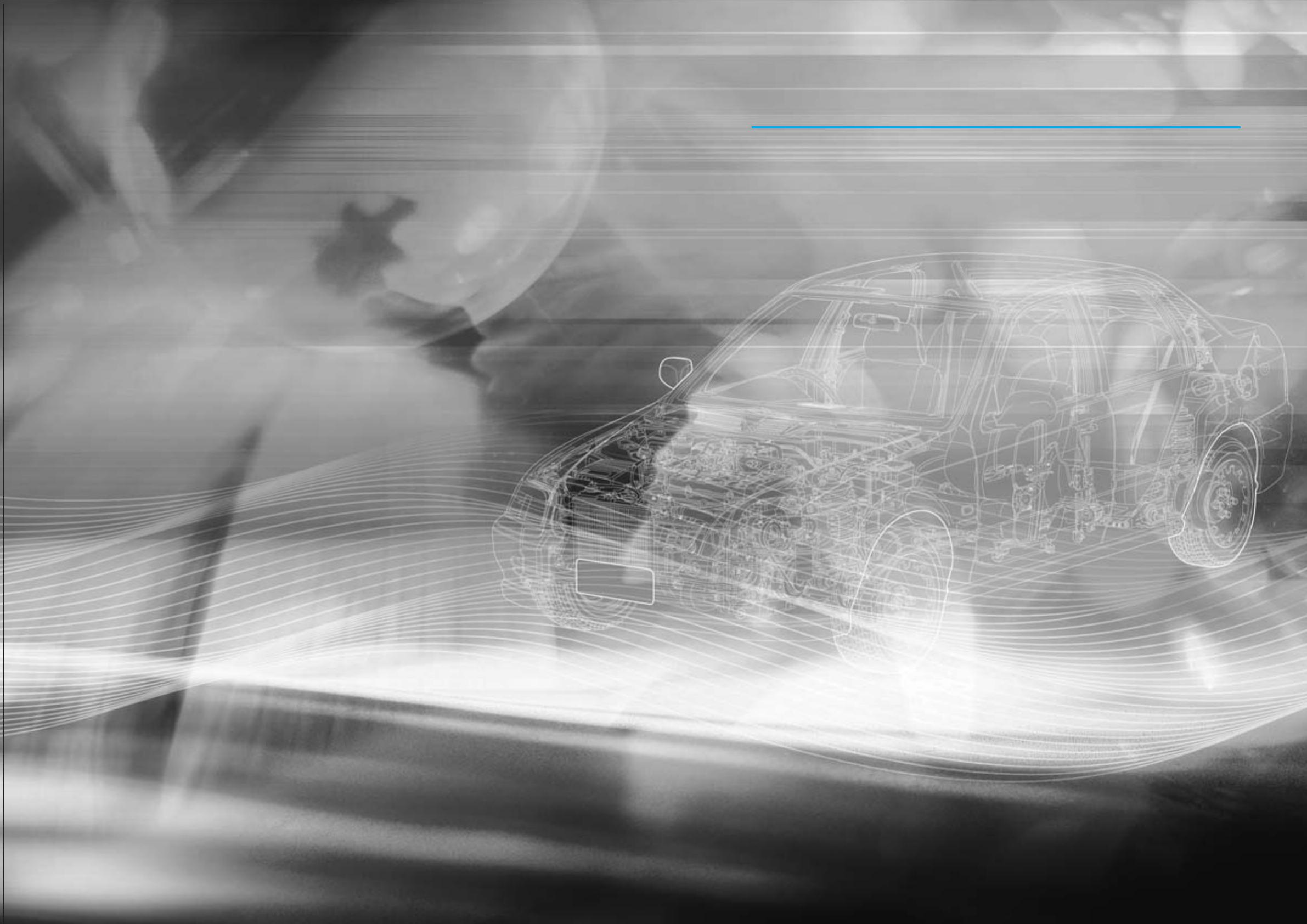
Combining vivid images and realistic sound
Combining vivid images and realistic sound
SANYO Car Audio
and
Automotive LAN Devices
SANYO Car Audio
and
Automotive LAN Devices
Automotive electronics is a field where advances
Automotive electronics is a field where advances
are occurring on a daily basis, notably with regard
are occurring on a daily basis, notably with regard
to the sound and information space realized through
to the sound and information space realized through
refined proprietary technologies.
refined proprietary technologies.
Automotive network technology controls many different
Automotive network technology controls many different
types of information such as automotive AV.
types of information such as automotive AV.
SANYO's LSIs powerfully support activities such as
SANYO's LSIs powerfully support activities such as
listening, watching, searching, and relaxing in this
listening, watching, searching, and relaxing in this
ubiquitous age, and support diverse needs with a
ubiquitous age, and support diverse needs with a
diversified product lineup and a broad array of
diversified product lineup and a broad array of
technologies.
The proprietary technologies of SANYO, a world leader
The proprietary technologies of SANYO, a world leader
in this field, are defining the present and near future of
in this field, are defining the present and near future of
automotive devices.
Automotive electronics is a field where advances
are occurring on a daily basis, notably with regard
to the sound and information space realized through
refined proprietary technologies.
Automotive network technology controls many different
types of information such as automotive AV.
SANYO's LSIs powerfully support activities such as
listening, watching, searching, and relaxing in this
ubiquitous age, and support diverse needs with a
diversified product lineup and a broad array of
technologies.
The proprietary technologies of SANYO, a world leader
in this field, are defining the present and near future of
automotive devices.
Combining vivid images and realistic sound
Automotive LAN
CARNET
CAN
MOST
Digital Radio System Chipsets
Digital Radio System Chipsets
1-chip Tuner
Tuner/IF-DSP
Car Audio DSP System Chipsets
Car Audio DSP System Chipsets
Car Audio DSP
Dolby Headphone IC
Car Audio CD/MP3/WMA System Chipsets
Car Audio CD/MP3/WMA System Chipsets
Super System-on-Chip Digital Servo IC with On-Chip RF System
Super System-on-Chip Digital Servo IC with On-Chip RF System
Compact Disc Player MP3 Decoder
Compact Disc Player MP3 Decoder
WMA Decoder
7.5 Mbps Automotive LAN Transceiver
7.5 Mbps Automotive LAN Transceiver
POF 50Mbps Automotive LAN
POF 50Mbps Automotive LAN
CAN Transceiver
Microcontrollers
Four-Channel Driver IC for CD Player/Decks
Four-Channel Driver IC for CD Player/Decks
Five-Channel Driver IC for CD Player/Decks
Five-Channel Driver IC for CD Player/Decks
DVD-ROM Spindle Motor Driver IC
DVD-ROM Spindle Motor Driver IC
System Motor Driver IC for CD and MD Players
System Motor Driver IC for CD and MD Players
Car Audio Built-in PLL Tuner System Chipsets (1)
Car Audio Built-in PLL Tuner System Chipsets (1)
Bus Control Tuner IC
Clear Surround Control IC Includes Plus Sound Algorithm
Clear Surround Control IC Includes Plus Sound Algorithm
Car Audio Electronic Volume Control IC with BBE Sound Processor
Car Audio Electronic Volume Control IC with BBE Sound Processor
Four Channel High-Output Line Amplifier for Car Audio
Four Channel High-Output Line Amplifier for Car Audio
Car Audio Built-in PLL Tuner System Chipsets (2)
Car Audio Built-in PLL Tuner System Chipsets (2)
Car Audio Tuner IC with Built-in PLL Circuit
Car Audio Tuner IC with Built-in PLL Circuit
Electronic Volume and Tone Control IC for Car Audio Systems
Electronic Volume and Tone Control IC for Car Audio Systems
Power Amplifier
Car Audio Standard Tuner System Chipsets
Car Audio Standard Tuner System Chipsets
System-on-Chip Tuner IC for Car Stereo Systems
System-on-Chip Tuner IC for Car Stereo Systems
Electronic Tuning ETR Controllers
Electronic Tuning ETR Controllers
Multiplexed Stereo Decoder System Chipsets
Multiplexed Stereo Decoder System Chipsets
Car Stereo 17 W Two-Channel BTL AF Amplifier
Car Stereo 17 W Two-Channel BTL AF Amplifier
Car Stereo 20 W Two-Channel BTL AF Amplifier
Car Stereo 20 W Two-Channel BTL AF Amplifier
Car Radio/Car Stereo 5 W Two-Channel Power Amplifier that Requires Minimal External Components
Car Radio/Car Stereo 5 W Two-Channel Power Amplifier that Requires Minimal External Components
Car Radio/Car Stereo 5 W Power Amplifier that Requires Minimal External Components
Car Radio/Car Stereo 5 W Power Amplifier that Requires Minimal External Components
FM Multiplex Broadcasting System Chipsets
FM Multiplex Broadcasting System Chipsets
Mobile FM Multiplex Broadcast (DARC System) Receiver IC
Mobile FM Multiplex Broadcast (DARC System) Receiver IC
Mobile FM Multiplex Broadcast Receiver IC with Built-in VICS Decoder
Mobile FM Multiplex Broadcast Receiver IC with Built-in VICS Decoder
RDS System Chipsets
Car Audio Electronic Tuning PLL Frequency Synthesizer
Car Audio Electronic Tuning PLL Frequency Synthesizer
RDS Signal-Processing System-on-Chip IC
RDS Signal-Processing System-on-Chip IC
RDS Demodulator ICs
Single-Chip RDS Signal Processing System IC
Single-Chip RDS Signal Processing System IC
Package Dimensions
.....................................................................................................................................................
1 to 2
......................................................................................................................................................................3 to 4
....................................................................................................................................................................................5
.................................................................................................................................................................................6
........................................................................................................................
7 to 8
.......................................................................................................................................................................9
...................................................................................................................................................................10
...............................................................................................................
11 to 12
................................................................................................................................................................13
.......................................................................................................................................................14
............................................................................................
15 to 16
.............................................................................17
..............................................................................................................................18
..................................................................................................................................................................19
.........................................................................................................................20
.......................................................................................................................................21
.............................................................................................................................................................22
......................................................................................................................................................23 to 26
......................................................................................................27 to 30
................................................................................................................31
...............................................................................................................................32
.................................................................................................33 to 34
...........................................................................
35 to 36
......................................................................................................................................................37
.........................................................................................38
........................................................................39
..............................................................................................40
...........................................................................
41 to 42
.................................................................................................................43
.......................................................................44 to 46
......................................................................................................................................................47 to 48
.......................................................................................
49 to 50
......................................................................................................51
.......................................................................................................................52 to 54
...................................................................................
55 to 56
........................................................................................................57
........................................................................................................58
..............59
......................................60
.....................................................................................
61 to 62
............................................................................63 to 64
..........................................................65 to 66
....................................................................................................................................
67 to 68
.......................................................................................... 69
.................................................................................................................70
....................................................................................................................................................71
...........................................................................................................72
......................................................................................................................................
73 to 78
Automotive LAN
CARNET
CAN
MOST
Digital Radio System Chipsets
1-chip Tuner
Tuner/IF-DSP
Car Audio DSP System Chipsets
Car Audio DSP
Dolby Headphone IC
Car Audio CD/MP3/WMA System Chipsets
Super System-on-Chip Digital Servo IC with On-Chip RF System
Compact Disc Player MP3 Decoder
WMA Decoder
7.5 Mbps Automotive LAN Transceiver
POF 50Mbps Automotive LAN
CAN Transceiver
Microcontrollers
Four-Channel Driver IC for CD Player/Decks
Five-Channel Driver IC for CD Player/Decks
DVD-ROM Spindle Motor Driver IC
System Motor Driver IC for CD and MD Players
Car Audio Built-in PLL Tuner System Chipsets (1)
Bus Control Tuner IC
Clear Surround Control IC Includes Plus Sound Algorithm
Car Audio Electronic Volume Control IC with BBE Sound Processor
Four Channel High-Output Line Amplifier for Car Audio
Car Audio Built-in PLL Tuner System Chipsets (2)
Car Audio Tuner IC with Built-in PLL Circuit
Electronic Volume and Tone Control IC for Car Audio Systems
Power Amplifier
Car Audio Standard Tuner System Chipsets
System-on-Chip Tuner IC for Car Stereo Systems
Electronic Tuning ETR Controllers
Multiplexed Stereo Decoder System Chipsets
Car Stereo 17 W Two-Channel BTL AF Amplifier
Car Stereo 20 W Two-Channel BTL AF Amplifier
Car Radio/Car Stereo 5 W Two-Channel Power Amplifier that Requires Minimal External Components
Car Radio/Car Stereo 5 W Power Amplifier that Requires Minimal External Components
FM Multiplex Broadcasting System Chipsets
Mobile FM Multiplex Broadcast (DARC System) Receiver IC
Mobile FM Multiplex Broadcast Receiver IC with Built-in VICS Decoder
RDS System Chipsets
Car Audio Electronic Tuning PLL Frequency Synthesizer
RDS Signal-Processing System-on-Chip IC
RDS Demodulator ICs
Single-Chip RDS Signal Processing System IC
Package Dimensions


