
Mobile Intel
®
Celeron
®
Processor on
.13 Micron Process in Micro-FCPGA
Package
Specification Update
October 2005
Notice: The mobile Intel
®
Celeron
®
processor may contain design defects or errors known as
errata which may cause the product to deviate from published specifications. Current
characterized errata are documented in this Specification Update.
Document Number: 251309-028

R
2 Specification Update
INFORMATION IN THIS DOCUMENT IS PROVIDED IN CONNECTION WITH INTEL
®
PRODUCTS. NO LICENSE, EXPRESS OR IMPLIED, BY
ESTOPPEL OR OTHERWISE, TO ANY INTELLECTUAL PROPERTY RIGHTS IS GRANTED BY THIS DOCUMENT. EXCEPT AS PROVIDED IN
INTEL’S TERMS AND CONDITIONS OF SALE FOR SUCH PRODUCTS, INTEL ASSUMES NO LIABILITY WHATSOEVER, AND INTEL DISCLAIMS
ANY EXPRESS OR IMPLIED WARRANTY, RELATING TO SALE AND/OR USE OF INTEL PRODUCTS INCLUDING LIABILITY OR WARRANTIES
RELATING TO FITNESS FOR PARTICULAR PURPOSE, MERCHANTABILITY OR INFRINGEMENT OR ANY PATENT, COPYRIGHT OR OTHER
INTELLECTUAL PROPERTY RIGHT. Intel products are not intended for use in medical, life saving, or life sustaining applications.
Intel may make changes to specifications and product descriptions at any time, without notice.
Designers must not rely on the absence or characteristics of any features or instructions marked “reserved” or “undefined.” Intel reserves these for future
definition and shall have no responsibility whatsoever for conflicts or incompatibilities arising from future changes to them.
The Mobile Intel
®
Celeron
®
processor may contain design defects or errors known as errata which may cause the product to deviate from published
specifications. Current characterized errata are available on request.
†
Hyper-Threading Technology requires a computer system with a Mobile Intel Pentium 4 Processor, a chipset and BIOS that utilize this technology, and an
operating system that includes optimizations for this technology. Performance will vary depending on the specific hardware and software you use. See
http://www.intel.com/info/hyperthreading for information.
Contact your local Intel sales office or your distributor to obtain the latest specifications and before placing your product order.
Intel, Pentium, Celeron, Intel Xeon, Intel SpeedStep, Intel NetBurst and the Intel logo are trademarks or registered trademarks of Intel Corporation or its
subsidiaries in the United States and other countries.
*Other names and brands may be claimed as the property of others.
Copyright © Intel Corporation 2002-2005. All rights reserved.

R
Specification Update 3
Contents
Revision History............................................................................................................................4
Preface .........................................................................................................................................6
Summary of Changes...................................................................................................................8
Identification Information ............................................................................................................12
Errata..........................................................................................................................................15
Specification Clarifications..........................................................................................................34
Specification Changes................................................................................................................37
Documentation Changes............................................................................................................40

R
4 Specification Update
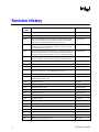
Revision History
Revision
Number
Description Date
-001 Initial Release June 2002
-002 Updated Identification Information table. August 2002
-003 Updated Documentation Change summary by removing old items that
have been incorporated into the Software Developer’s Manual; Added
errata V30-V32; Added Documentation Changes V3-V24.
September 2002
-004 Updated Summary of Changes; Added prefix letter W; Removed
previous errata V32 as not applicable, added new errata V32; Added
Documentation Changes V25-V32.
October 2002
-005 Added errata V33; Added Spec Clarification V1; Added Spec Change V1;
Removed Documentation Changes that have been incorporated into the
Software Developer’s Manual; Added a note in Documentation Changes.
November 2002
-006 No new Errata, Documentation Change, Spec Clarification, or Spec
Change. Updated note concerning the Software Developer’s Manual.
December 2002
-007 Added Erratum V34. Updated summary tables to include C1 step. January 2003
-008 Added Erratum V35. February 2003
-009 Updated Erratum V34, added new Erratum V36 March 2003
-010 Updated codes used in summary tables. Updated errata summary table
entry for V27, V28, V34, & V36. Updated tables for D1-step
April 2003
-011 Added info for C-1 step 1.6 GHz to 2.2 GHz to Table 1. May 2003
-012 Updated Erratum V33. Added identification info for D-1 step 2.4 GHz.
Updated summary table code Z.
June 2003
-013 Added Erratum V37. July 2003
-014 Added V2 Specification Change. Added Errata V38. August 2003
-015 Added Errata V39 and V40. September 2003
-016 Added Errata V41. October 2003
-017 Updated Errata V41. November 2003
-018 Updated Errata V42. March 2004
-019 Updated Errata V6. April 2004
-020 Updated Errata V11. Added Errata V43. May 2004
-021 Added Errata V44. Updated Processor Identification Information June 2004
-022 Added Errata V45. September 2004
-023 Added Errata V46-47 October 2004
-024 Added errata V48 November 2004
-025 Added errata V49 December 2004
-026 Added Specification Clarification V2 May 2005

R
Specification Update 5
-027 Updated Related Documents table July 2005
-028 Added errata V50 and updated Processor Identification Table. October 2005

R
6 Specification Update
Preface
This document is an update to the specifications contained in the document listed in the following
Affected/Related Documents table. It is a compilation of device and document errata and specification
clarifications and changes, and is intended for hardware system manufacturers and for software
developers of applications, operating system, and tools.
Information types defined in the Nomenclature section of this document are consolidated into this update
document and are no longer published in other documents. This document may also contain information
that has not been previously published.
Affected Documents
Document Title Document Number
Mobile Intel
®
Celeron
®
Processor on .13 Micron Process in Micro-
FCPGA Package Datasheet
251308
Related Documents
Document Title Document Number
IA-32 Intel
®
Architecture Software Developer's Manual, Volume 1:
Basic Architecture
253665
IA-32 Intel
®
Architecture Software Developer's Manual, Volume
2A: Instruction Set Reference, A-M
253666
IA-32 Intel
®
Architecture Software Developer's Manual, Volume
2B: Instruction Set Reference, N-Z
253667
IA-32 Intel
®
Architecture Software Developer's Manual, Volume 3:
System Programming Guide
253668

R
Specification Update 7
Nomenclature
S-Spec Number is a five-digit code used to identify products. Products are differentiated by their unique
characteristics, e.g., core speed, L2 cache size, package type, etc. as described in the processor
identification information table. Care should be taken to read all notes associated with each S-Spec
number.
Errata are design defects or errors. Errata may cause the mobile Intel Pentium 4 processor-m’s behavior
to deviate from published specifications. Hardware and software designed to be used with any given
processor must assume that all errata documented for that processor are present on all devices unless
otherwise noted.
Documentation Changes include typos, errors, or omissions from the current published specifications.
These changes will be incorporated in the next release of the specifications.
Specification Clarifications describe a specification in greater detail or further highlight a
specification’s impact to a complex design situation. These clarifications will be incorporated in the next
release of the specifications.
Specification Changes are modifications to the current published specifications for the Intel Pentium 4
processor. These changes will be incorporated in the next release of the specifications.

R
8 Specification Update
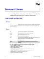
Summary of Changes
The following table indicates the Errata, Documentation Changes, Specification Clarifications, or
Specification Changes that apply to Intel Pentium 4 processors. Intel intends to fix some of the errata in
a future stepping of the component, and to account for the other outstanding issues through
documentation or specification changes as noted. This table uses the following notations:
Codes Used in Summary Table
Stepping
X: Erratum, Specification Change or Clarification that applies to this stepping.
(No mark) or (Blank Box): This erratum is fixed in listed stepping or specification change does not
apply to listed stepping.
Status
Doc: Document change or update that will be implemented.
PlanFix: This erratum may be fixed in a future of the product.
Fixed: This erratum has been previously fixed.
NoFix: There are no plans to fix this erratum.
PKG: This column refers to errata on the Mobile Intel
®
Celeron
®
Processor on .13
Micron Process in Micro-FCPGA Package
substrate.
AP: APIC related erratum.
Shaded: This item is either new or modified from the previous version of the
document.
Each Specification Update item is prefixed with a capital letter to distinguish the product. The key
below details the letters that are used in Intel’s microprocessor Specification Updates:
A = Intel ® Pentium ® II processor
B = Mobile Intel ® Pentium ® II processor
C = Intel ® Celeron ® processor
E = Intel ® Pentium ® III processor
F = Intel® Pentium® processor Extreme Edition and Intel® Pentium® D processor
G = Intel ® Pentium ® III Xeon™ processor
H = Mobile Intel ® Celeron ® processor at 466/433/400/366/333/300 and 266 MHz
J = 64-bit Intel® Xeon™ processor MP with 1MB L2 Cache
K = Mobile Intel ® Pentium ® III processor

R
Specification Update 9
L = Intel ® Celeron ® D processor
M = Mobile Intel ® Celeron ® processor
N = Intel ® Pentium ® 4 processor
O = Intel ® Xeon™ processor MP
P = Intel ® Xeon™ processor
Q = Mobile Intel
®
Pentium
®
4 processor supporting Hyper-Threading Technology on 90-nm process
technology
R = Intel® Pentium® 4 processor on 90 nm process
S = 64-bit Intel® Xeon™ processor with 800 MHz system bus (1 MB and 2 MB L2 cache versions)
T = Mobile Intel® Pentium® 4 processor-M
V = Mobile Intel® Celeron® processor on .13 Micron Process in Micro-FCPGA Package
W= Intel® Celeron® M processor
X = Intel
®
Pentium
®
M processor on 90nm process with 2-MB L2 Cache
Y = Intel® Pentium® M processor
Z = Mobile Intel ® Pentium ® 4 processor with 533 MHz system bus
AC = Intel
®
Celeron® Processor in 478 Pin Package
The Specification Updates for the Pentium
®
processor, Pentium
®
Pro processor, and other Intel products
do not use this convention
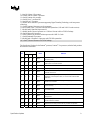
Steppings
NO.
B0 C1 D1
Plans ERRATA
V1 X X X NoFix
I/O restart in SMM may fail after simultaneous machine check
exception (MCE)
V2 X X X NoFix
MCA registers may contain invalid information if RESET# occurs and
PWRGOOD is not held asserted
V3 X X X NoFix Transaction is not retried after BINIT#
V4 X X X NoFix Invalid opcode 0FFFh requires a ModRM byte
V5 X X X NoFix
FSW may not be completely restored after page fault on FRSTOR or
FLDENV instructions
V6 X X X NoFix
The Processor Signals Page-Fault Exception (#PF) Instead of
Alignment Check Exception (#AC) on an Unlocked CMPXCHG8B
Instruction
V7 X X X NoFix
When in no-fill mode the memory type of large pages are incorrectly
forced to uncacheable
V8 X X X NoFix
Processor may hang due to speculative page walks to non-existent
system memory
V9 X X X NoFix
The IA32_MC1_STATUS register may contain incorrect information for
correctable errors
V10 X X X NoFix Debug mechanisms may not function as expected
V11 X X X NoFix
Machine check architecture error reporting and recovery may not work
as expected
V12 X X X NoFix
Cascading of performance counters does not work correctly when
forced overflow is enabled
V13 X X X NoFix EMON event counting of x87 loads may not work as expected
V14 X X X NoFix Speculative page fault may cause livelock

R
10 Specification Update
Steppings
NO.
B0 C1 D1
Plans ERRATA
V15 X
Fixed
Incorrect data may be returned when page tables are in Write
Combining (WC) memory space
V16 X
X X
NoFix
Processor issues inconsistent transaction size attributes for locked
operation
V17 X
Fixed
Multiple accesses to the same S-state L2 cache line and ECC error
combination may result in loss of cache coherency
V18 Fixed Processor may hang when resuming from Deep Sleep state
V19 X X X NoFix
When the processor is in the System Management Mode (SMM),
debug registers may be fully writeable
V20 X X X NoFix
Associated counting logic must be configured when using Event
Selection Control (ESCR) MSR
V21 X X X NoFix
IA32_MC0_ADDR and IA32_MC0_MISC Registers Will Contain
Invalid or Stale Data Following a Data, Address, or Response Parity
Error
V22 X Fixed
CR2 May Be Incorrect or an Incorrect Page Fault Error Code May Be
Pushed Onto Stack After Execution of an LSS Instruction
V23 X
Fixed
BPM[5:3]# and GHI# V
IL
Do Not Meet Specification
V24 X
X X
NoFix
Processor May Hang Under Certain Frequencies and 12.5%
STPCLK# Duty Cycle
V25 X X X NoFix
System May Hang if a Fatal Cache Error Causes Bus Write Line
(BWL) Transaction to Occur to the Same Cache Line Address as an
Outstanding Bus Read Line (BRL) or Bus Read-Invalidate Line (BRIL)
V26 X
Fixed
L2 Cache May Contain Stale Data in the Exclusive State
V27 X
X
Fixed
Re-mapping the APIC Base Address to a Value Less Than or Equal to
0xDC001000 may Cause IO and Special Cycle Failure
V28 X
X
Fixed
Erroneous BIST Result Found in EAX Register After Reset
V29 X
Fixed
Processor Does not Flag #GP on Non-zero Write to Certain MSRs
V30 X X X NoFix
Simultaneous Assertion of A20M# and INIT# may Result in Incorrect
Data Fetch
V31 X X X PlanFix Processor Does not Respond to Break Requests From ITP
V32 X Fixed Processor Signature Returns Incorrect Number of ITLB Entries
V33 X X X NoFix
A Write to APIC Registers Sometimes May Appear to Have Not
Occurred
V34 X Fixed Store to Load Data Forwarding may Result in Switched Data Bytes
V35 X X X NoFix Parity Error in the L1 Cache may Cause the Processor to Hang
V36 X X Fixed
The TCK Input in the Test Access Port (TAP) is Sensitive to Low
Clock Edge Rates and Prone to Noise Coupling Onto TCK’s Rising or
Falling Edges
V37 X X X NoFix
The State of the Resume Flag (RF Flag) in a Task-State Segment
(TSS) May be Incorrect
V38 X X X NoFix
Changes to CR3 Register do not Fence Pending Instruction Page
Walks
V39 X X X NoFix
System Bus Interrupt Messages without Data that Receive a

R
Specification Update 11
Steppings
NO.
B0 C1 D1
Plans ERRATA
HardFailure Response May Hang the Processor
V40 X X X NoFix
Memory Type of the Load Lock Different from its Corresponding Store
Unlock
V41 X X X NoFix
A 16-bit Address Wrap Resulting from a Near Branch (Jump or Call)
May Cause an Incorrect Address to Be Reported to the #GP Exception
Handler
V42 X X X NoFix
Incorrect Debug Exception (#DB) May Occur When a Data Breakpoint
is set on an FP Instruction
V43 X X X NoFix xAPIC May Not Report Some Illegal Vector Errors
V44 X X X NoFix
Memory Aliasing of Pages as Uncacheable Memory Type and Write
Back (WB) May Hang the System
V45 X Plan Fix
A Timing Maginality in the Arithmetic Logic Unit (ALU) May Cause
Indeterminate Behavior
V46 X X X No Fix
With TF (Trap Flag) Asserted, FP Instruction That Triggers an
Unmasked FP Exception May Take Single Step Trap Before
Retirement of Instruction
V47 X X X No Fix
BTS(Branch Trace Store) and PEBS(Precise Event Based Sampling)
May Update Memory outside the BTS/PEBS Buffer
V48 X X X No Fix
Memory Ordering Failure May Occur with Snoop Filtering Third-Party
Agents after Issuing and Completing a BWIL (Bus Write Invalidate
Line) or BLW (Bus Locked Write) Transaction
V49 X X X No Fix
Control Register 2 (CR2) Can be Updated during a REP MOVS/STOS
Instruction with Fast Strings Enabled
V50 X X X No Fix
Writing the Local Vector Table (LVT) when an Interrupt is Pending May
Cause an Unexpected Interrupt
Number SPECIFICATION CHANGE
V1 Context ID feature added to CPUID Feature/IA32_MISC_Enable Registers
V2 BR0# Maximum Hold Time Specification Change
Number SPECIFICATION CLARIFICATIONS
V1 Clarifying DBI# Definition for all Processors with Intel NetBurst
®
Microarchitecture
V2 Specification Clarification with respect to Time-stamp Counter
Number DOCUMENTATION CHANGES
There are no Documentation Changes in this Specification Update revision.

R
12 Specification Update
Identification Information
The mobile Intel
®
Celeron
®
processor on .13 micron process in Micro-FCPGA package can be identified
by the following values:
Family
1
Model
2
Brand ID
3
1111 0010 00001000
4
1111 0010 00001111
5
NOTES:
1. The Family corresponds to bits [11:8] of the EDX register after Reset, bits [11:8] of the EAX register after the
CPUID instruction is executed with a 1 in the EAX register, and the generation field of the Device ID register
accessible through Boundary Scan.
2. The Model corresponds to bits [7:4] of the EDX register after Reset, bits [7:4] of the EAX register after the
CPUID instruction is executed with a 1 in the EAX register, and the model field of the Device ID register
accessible through Boundary Scan.
3. The Brand ID corresponds to bits [7:0] of the EBX register after the CPUID instruction is executed with a 1 in
the EAX register.
4. This brand id MUST be used in conjunction with CPUID = 0F24h.
5. This brand id MUST be used in conjunction with CPUID = 0F27h.

R
Specification Update 13
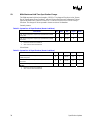
Table 1. Mobile Intel
®
Celeron
®
Processor Identification Information
S-Spec
Product
Stepping
L2
Cache
Size
(bytes)
CPU
Signature
Core Frequency
Bus
Frequency
Voltage Package Notes
SL6FM B0 256 K 0F24h 1.4 GHz 400 MHz 1.3 V Micro-FCPGA 1
SL6FN B0 256 K 0F24h 1.5 GHz 400 MHz 1.3 V Micro-FCPGA 1
SL6M4 C1 256 K 0F27h 1.4 GHz 400 MHz 1.3 V Micro-FCPGA
SL6M5 C1 256 K 0F27h 1.5 GHz 400 MHz 1.3 V Micro-FCPGA
SL6J2 C1 256 K 0F27h 1.6 GHz 400 MHz 1.3 V Micro-FCPGA
SL6J3 C1 256 K 0F27h 1.7 GHz 400 MHz 1.3 V Micro-FCPGA
SL6J4 C1 256 K 0F27h 1.8 GHz 400 MHz 1.3 V Micro-FCPGA
SL6QH C1 256 K 0F27h 2.0 GHz 400 MHz 1.3 V Micro-FCPGA
SL6ZW C1 256 K 0F27h 2.2 GHz 400 MHz 1.3 V Micro-FCPGA
SL7MG D1 256K 0F29h 1.2 GHz 400 MHz 1.3 V Micro-FCPGA
2
SL6VG D1 256 K 0F29h 1.70 GHz 400 MHz 1.3 V Micro-FCPGA
SL6VH D1 256 K 0F29h 1.80 GHz 400 MHz 1.3 V Micro-FCPGA
SL6VJ D1 256 K 0F29h 2.00 GHz 400 MHz 1.3 V Micro-FCPGA
SL73Y D1 256 K 0F29h 2.20 GHz 400 MHz 1.3 V Micro-FCPGA
SL75J D1 256 K 0F29h 2.40 GHz 400 MHz 1.3 V Micro-FCPGA
NOTES:
1. Based on B0-Shrink process.
2. Supported by the Embedded Intel Architecture Division

R
14 Specification Update
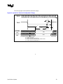
Component Marking Information
Figure 1. Mobile Intel
®
Celeron
®
Processor on .13 Micron Process (Micro-FCPGA) Markings
FFFFFFFF S/N
PRODUCT DETAIL
2D Matrix
(supplier Lot ID + SER#)
LEGAL REQUIREMENTS
S-SPEC COO
INTEL m c ‘01
FPO#
S-Spec
#
§

R
Specification Update 15
Errata
V1. I/O Restart in SMM may Fail after Simultaneous Machine Check Exception (MCE)
Problem: If an I/O instruction (IN, INS, REP INS, OUT, OUTS, or REP OUTS) is being executed, and if the data
for this instruction becomes corrupted, the processor will signal a Machine Check Exception (MCE). If
the instruction is directed at a device that is powered down, the processor may also receive an assertion
of SMI#. Since MCEs have higher priority, the processor will call the MCE handler, and the SMI#
assertion will remain pending. However, upon attempting to execute the first instruction of the MCE
handler, the SMI# will be recognized and the processor will attempt to execute the SMM handler. If the
SMM handler is completed successfully, it will attempt to restart the I/O instruction, but will not have
the correct machine state, due to the call to the MCE handler.
Implication: A simultaneous MCE and SMI# assertion may occur for one of the I/O instructions above. The SMM
handler may attempt to restart such an I/O instruction, but will have an incorrect state due to the MCE
handler call, leading to failure of the restart and shutdown of the processor.
Workaround: If a system implementation must support both SMM and board I/O restart, the first thing the SMM
handler code should do is check for a pending MCE. If there is an MCE pending, the SMM handler
should immediately exit via an RSM instruction and allow the MCE handler to execute. If there is no
MCE pending, the SMM handler may proceed with its normal operation.
Status: For the steppings affected, see the Summary Tables of Changes.
V2. MCA Registers May Contain Invalid Information if RESET# Occurs and
PWRGOOD Is Not Held Asserted
Problem: This erratum can occur as a result either of the following events:
• PWRGOOD is de-asserted during a RESET# assertion causing internal glitches that may result in
the possibility that the MCA registers latch invalid information.
• Or during a reset sequence if the processor’s power remains valid regardless of the state of
PWRGOOD, and RESET# is re-asserted before the processor has cleared the MCA registers, the
processor will begin the reset process again but may not clear these registers.
Implication: When this erratum occurs, the information in the MCA registers may not be reliable.
Workaround: Ensure that
PWRGOOD remains asserted throughout any RESET# assertion and that RESET# is not re-
asserted while PWRGOOD is de-asserted.
Status: For the steppings affected, see the Summary Tables of Changes.

R
16 Specification Update
V3.
Transaction Is Not Retried after BINIT#
Problem: If the first transaction of a locked sequence receives a HITM# and DEFER# during the snoop phase it
should be retried and the locked sequence restarted. However, if BINIT# is also asserted during this
transaction, it will not be retried.
Implication: When this erratum occurs, locked transactions will unexpectedly not be retried.
Workaround: None identified
Status: For the steppings affected, see the Summary Tables of Changes.
V4.
Invalid Opcode 0FFFh Requires a ModRM Byte
Problem: Some invalid opcodes require a ModRM byte (or other following bytes), while others do not. The
invalid opcode 0FFFh did not require a ModRM byte in previous generation Intel architecture
processors, but does in the Intel
®
Pentium
®
4 processor.
Implication: The use of an invalid opcode 0FFFh without the ModRM byte may result in a page or limit fault on the
Intel
®
Pentium
®
4 processor.
Workaround: Use a ModRM byte with invalid 0FFFh opcode.
Status: For the steppings affected, see the Summary Tables of Changes.
V5.
FSW May Not Be Completely Restored after Page Fault on FRSTOR or FLDENV
Instructions
Problem: If the FPU operating environment or FPU state (operating environment and register stack) being loaded
by an FLDENV or FRSTOR instruction wraps around a 64Kbyte or 4Gbyte boundary and a page fault
(#PF) or segment limit fault (#GP or #SS) occurs on the instruction near the wrap boundary, the upper
byte of the FPU status word (FSW) might not be restored. If the fault handler does not restart program
execution at the faulting instruction, stale data may exist in the FSW.
Implication: When this erratum occurs, stale data will exist in the FSW.
Workaround: Ensure that the FPU operating environment and FPU state do not cross 64Kbyte or 4Gbyte boundaries.
Alternately, ensure that the page fault handler restarts program execution at the faulting instruction after
correcting the paging problem.
Status: For the steppings affected, see the Summary Tables of Changes.

R
Specification Update 17
V6.
The Processor Signals Page-Fault Exception (#PF) Instead of Alignment Check
Exception (#AC) on an Unlocked CMPXCHG8B Instruction
Problem: If a Page-Fault Exception (#PF) and Alignment Check Exception (#AC) both occur for an unlocked
CMPXCHG8B instruction, then #PF will be flagged.
Implication: Software that depends on the Alignment Check Exception (#AC) before the Page-Fault Exception (#PF)
will be affected since #PF is signaled in this case.
Workaround: Remove the software’s dependency on #AC having precedence over #PF. Alternately, correct the page
fault in the page fault handler and then restart the faulting instruction.
Status: For the steppings affected, see the Summary Tables of Changes
V7.
When in No-Fill Mode the Memory Type of Large Pages are Incorrectly Forced to
Uncacheable
Problem: When the processor is operating in No-Fill Mode (CR0.CD=1), the paging hardware incorrectly forces
the memory type of large (PSE-4M and PAE-2M) pages to uncacheable (UC) memory type regardless of
the MTRR settings. By forcing the memory type of these pages to UC, load operations, which should hit
valid data in the L1 cache, are forced to load the data from system memory. Some applications will lose
the performance advantage associated with the caching permitted by other memory types.
Implication: This erratum may result in some performance degradation when using no-fill mode with large pages.
Workaround: None identified
Status: For the steppings affected, see the Summary Tables of Changes.
V8.
Processor May Hang Due to Speculative Page Walks to Non-Existent System
Memory
Problem: A load operation that misses the Data Translation Lookaside Buffer (DTLB) will result in a page-walk.
If the page-walk loads the Page Directory Entry (PDE) from cacheable memory and that PDE load
returns data that points to a valid Page Table Entry (PTE) in uncacheable memory the processor will
access the address referenced by the PTE. If the address referenced does not exist the processor will
hang with no response from system memory.
Implication: Processor may hang due to speculative page walks to non-existent system memory.
Workaround: Page directories and page tables in UC memory space that are marked valid must point to physical
addresses that will return a data response to the processor.
Status: For the steppings affected, see the Summary Tables of Changes.

R
18 Specification Update
V9.
The IA32_MC1_STATUS Register May Contain Incorrect Information for
Correctable Errors
Problem: When a speculative load operation hits the L2 cache and receives a correctable error, the
IA32_MC1_STATUS register may be updated with incorrect information. The IA32_MC1_STATUS
register should not be updated for speculative loads.
Implication: When this erratum occurs, the IA32_MC1_STATUS register will contain incorrect information for
correctable errors.
Workaround: None identified
Status: For the steppings affected, see the Summary Tables of Changes.
V10.
Debug Mechanisms May Not Function As Expected
Problem: Certain debug mechanisms may not function as expected on the processor. The cases are as follows:
• When the following conditions occur: 1) An FLD instruction signals a stack overflow or
underflow, 2) the FLD instruction splits a page-boundary or a 64 byte cache line boundary, 3) the
instruction matches a Debug Register on the high page or cache line respectively, and 4) the FLD
has a stack fault and a memory fault on a split access, the processor will only signal the stack fault
and the debug exception will not be taken.
• When a data breakpoint is set on the ninth and/or tenth byte(s) of a floating point store using the
Extended Real data type, and an unmasked floating point exception occurs on the store, the break
point will not be captured.
• When any instruction has multiple debug register matches, and any one of those debug registers is
enabled in DR7, all of the matches should be reported in DR6 when the processor goes to the
debug handler. This is not true during a REP instruction. As an example, during execution of a
REP MOVSW instruction the first iteration a load matches DR0 and DR2 and sets DR6 as
FFFF0FF5h. On a subsequent iteration of the instruction, a load matches only DR0. The DR6
register is expected to still contain FFFF0FF5h, but the processor will update DR6 to FFFF0FF1h.
• A Data breakpoint that is set on a load to uncacheable memory may be ignored due to an internal
segment register access conflict. In this case the system will continue to execute instructions,
bypassing the intended breakpoint. Avoiding having instructions that access segment descriptor
registers, e.g., LGDT, LIDT close to the UC load, and avoiding serialized instructions before the
UC load will reduce the occurrence of this erratum.
Implication: Certain debug mechanisms do not function as expected on the processor.
Workaround: None identified
Status: For the steppings affected, see the Summary Tables of Changes.

R
Specification Update 19
V11.
Machine Check Architecture Error Reporting and Recovery May Not Work As
Expected
Problem: When the processor detects errors it should attempt to report and/or recover from the error. In the
situations described below, the processor does not report and/or recover from the error(s) as intended. -
When a transaction is deferred during the snoop phase and subsequently receives a Hard Failure
response, the transaction should be removed from the bus queue so that the processor may proceed.
Instead, the transaction is not properly removed from the bus queue, the bus queue is blocked, and the
processor will hang.
- When a hardware prefetch results in an uncorrectable tag error in the L2 cache,
MC0_STATUS.UNCOR and MC0_STATUS.PCC are set but no Machine Check Exception (MCE) is
signaled. No data loss or corruption occurs because the data being prefetched has not been used. If the
data location with the uncorrectable tag error is subsequently accessed, an MCE will occur. However,
upon this MCE, or any other subsequent MCE, .the information for that error will not be logged because
MC0_STATUS.UNCOR has already been set and the MCA status registers will not contain information
about the error which caused the MCE assertion but instead will contain information about the prefetch
error event.
- When the reporting of errors is disabled for Machine Check Architecture (MCA) Bank 2 by setting all
MC2_CTL register bits to 0, uncorrectable errors should be logged in the IA32_MC2_STATUS register
but no machine-check exception should be generated. Uncorrectable loads on bank 2, which would
normally be logged in the IA32_MC2_STATUS register, are not logged.
- When one half of a 64 byte instruction fetch from the L2 cache has an uncorrectable error and the other
32 byte half of the same fetch from the L2 cache has a correctable error, the processor will attempt to
correct the correctable error but cannot proceed due to the uncorrectable error. When this occurs the
processor will hang.
-When an L1 cache parity error occurs, the cache controller logic should write the physical address of
the data memory location that produced that error into the IA32_MC1_ADDR REGISTER
(MC1_ADDR). In some instances of a parity error on a load operation that hits the L1 cache, the cache
controller logic may write the physical address from a subsequent load or store operation into the
IA32_MC1_ADDR register.
- When an error exists in the tag field of a cache line such that a request for ownership (RFO) issued by
the processor hits multiple tag fields in the L2 cache (the correct tag and the tag with the error) and the
accessed data also has a correctable error, the processor will correctly log the multiple tag match error
but will hang when attempting to execute the machine check exception handler.
- If a memory access receives a machine check error on both 64 byte halves of a 128-byte L2 cache
sector, the IA32_MC0_STATUS register records this event as multiple errors, i.e., the valid error bit and
the overflow error bit are both set indicating that a machine check error occurred while the results of a
previous error were in the error-reporting bank. The IA32_MC1_STATUS register should also record
this event as multiple errors but instead records this event as only one correctable error.
- The overflow bit should be set to indicate when more than one error has occurred. The overflow bit
being set indicates that more than one error has occurred. Because of this erratum, if any further errors
occur, the MCA overflow bit will not be updated, thereby incorrectly indicating only one error has been
received.
- If an I/O instruction (IN, INS, REP INS, OUT, OUTS, or REP OUTS) is being executed, and if the
data for this instruction becomes corrupted, the processor will signal a Machine Check Exception
(MCE). If the instruction is directed at a device that is powered down, the processor may also receive an
assertion of SMI#. Since MCEs have higher priority, the processor will call the MCE handler, and the
SMI# assertion will remain pending. However, while attempting to execute the first instruction of the
MCE handler, the SMI# will be recognized and the processor will attempt to execute the SMM handler.
If the SMM handler is successfully completed, it will attempt to restart the I/O instruction, but will not
have the correct machine state due to the call to the MCE handler. This can lead to failure of the restart
and shutdown of the processor.
- If PWRGOOD is de-asserted during a RESET# assertion causing internal glitches, the MCA registers

R
20 Specification Update
may latch invalid information.
- If RESET# is asserted, then de-asserted, and reasserted, before the processor has cleared the MCA
registers, then the information in the MCA registers may not be reliable, regardless of the state or state
transitions of PWRGOOD.
- If MCERR# is asserted by one processor and observed by another processor, the observing processor
does not log the assertion of MCERR#. The Machine Check Exception (MCE) handler called upon
assertion of MCERR# will not have any way to determine the cause of the MCE.
- The Overflow Error bit (bit 62) in the IA32_MC0_STATUS register indicates, when set, that a
machine check error occurred while the results of a previous error were still in the error reporting bank
(i.e. The Valid bit was set when the new error occurred). If an uncorrectable error is logged in the error-
reporting bank and another error occurs, the overflow bit will not be set.
- The MCA Error Code field of the IA32_MC0_STATUS register gets written by a different mechanism
than the rest of the register. For uncorrectable errors, the other fields in the IA32_MC0_STATUS
register are only updated by the first error. Any further errors that are detected will update the MCA
Error Code field without updating the rest of the register, thereby leaving the IA32_MC0_STATUS
register with stale information.
- When a speculative load operation hits the L2 cache and receives a correctable error, the
IA32_MC1_Status Register may be updated with incorrect information. The IA32_MC1_Status Register
should not be updated for speculative loads.
- The processor should only log the address for L1 parity errors in the IA32_MC1_Status register if a
valid address is available. If a valid address is not available, the Address Valid bit in the
IA32_MC1_Status register should not be set. In instances where an L1 parity error occurs and the
address is not available because the linear to physical address translation is not complete or an internal
resource conflict has occurred, the Address Valid bit is incorrectly set.
- The processor may hang when an instruction code fetch receives a hard failure response from the
system bus. This occurs because the bus control logic does not return data to the core, leaving the
processor empty. IA32_MC0_STATUS MSR does indicate that a hard fail response occurred.
- The processor may hang when the following events occur and the machine check exception is enabled,
CR4.MCE=1. A processor that has it's STPCLK# pin asserted will internally enter the Stop Grant State
and finally issue a Stop Grant Acknowledge special cycle to the bus. If an uncorrectable error is
generated during the Stop Grant process it is possible for the Stop Grant special cycle to be issued to the
bus before the processor vectors to the machine check handler. Once the chipset receives its last Stop
Grant special cycle it is allowed to ignore any bus activity from the processors. As a result, processor
accesses to the machine check handler may not be acknowledged, resulting in a processor hang.
Implication: The processor is unable to correctly report and/or recover from certain errors
Workaround: None identified.
Status: For the steppings affected, see the Summary Tables of Changes
V12.
Cascading of Performance Counters Does Not Work Correctly When Forced
Overflow Is Enabled
Problem: The performance counters are organized into pairs. When the CASCADE bit of the Counter
Configuration Control Register (CCCR) is set, a counter that overflows will continue to count in the
other counter of the pair. The FORCE_OVF bit forces the counters to overflow on every non-zero
increment. When the FORCE_OVF bit is set, the counter overflow bit will be set but the counter no
longer cascades.
Implication: The performance counters do not cascade when the FORCE_OVF bit is set.
Workaround: None identified
Status: For the steppings affected, see the Summary Tables of Changes.
Page is loading ...
Page is loading ...
Page is loading ...
Page is loading ...
Page is loading ...
Page is loading ...
Page is loading ...
Page is loading ...
Page is loading ...
Page is loading ...
Page is loading ...
Page is loading ...
Page is loading ...
Page is loading ...
Page is loading ...
Page is loading ...
Page is loading ...
Page is loading ...
Page is loading ...
Page is loading ...
-
 1
1
-
 2
2
-
 3
3
-
 4
4
-
 5
5
-
 6
6
-
 7
7
-
 8
8
-
 9
9
-
 10
10
-
 11
11
-
 12
12
-
 13
13
-
 14
14
-
 15
15
-
 16
16
-
 17
17
-
 18
18
-
 19
19
-
 20
20
-
 21
21
-
 22
22
-
 23
23
-
 24
24
-
 25
25
-
 26
26
-
 27
27
-
 28
28
-
 29
29
-
 30
30
-
 31
31
-
 32
32
-
 33
33
-
 34
34
-
 35
35
-
 36
36
-
 37
37
-
 38
38
-
 39
39
-
 40
40


Ask a question and I''ll find the answer in the document
Finding information in a document is now easier with AI
Related papers
-
Intel LE80537VE001512 Datasheet
-
-
-
-
-
Intel 4 3.20 GHz User manual
-
-
-
-
Other documents
-
Fujifilm S26361-F3099-L828 Datasheet
-
Kathrein 21610001 Datasheet
-
AMD K User manual
-
RAD Data comm BLW-04EX User manual
-
 Planex BRL-04AR User manual
-
Compaq 239158-999 - Mini Tower - Power Supply 250 Watt User manual
-
 Planex BRL-04EX User manual
-
-
 Planex Communications SJ9-BLW54CW3 User manual
-
Symphony V47 User manual


