
–
P80C31X2/32X2
P80C51X2/52X2/54X2/58X2
P87C51X2/52X2/54X2/58X2
80C51 8-bit microcontroller family
4K/8K/16K/32K ROM/OTP
128B/256B RAM
low voltage (2.7 to 5.5 V), low power, high speed (30/33 MHz)
Product data
Supersedes data of 2002 Sep 12
2003 Jan 24
INTEGRATED CIRCUITS

Philips Semiconductors Product data
P80C3xX2; P80C5xX2;
P87C5xX2
80C51 8-bit microcontroller family
4K/8K/16K/32K ROM/OTP, low voltage (2.7 to 5.5 V),
low power, high speed (30/33 MHz)
2
2003 Jan 24 853-2337 29260
DESCRIPTION
The Philips microcontrollers described in this data sheet are
high-performance static 80C51 designs incorporating Philips’
high-density CMOS technology with operation from 2.7 V to 5.5 V.
They support both 6-clock and 12-clock operation.
The P8xC31X2/51X2 and P8xC32X2/52X2/54X2/58X2 contain
128 byte RAM and 256 byte RAM respectively, 32 I/O lines, three
16-bit counter/timers, a six-source, four-priority level nested interrupt
structure, a serial I/O port for either multi-processor
communications, I/O expansion or full duplex UART, and on-chip
oscillator and clock circuits.
In addition, the devices are low power static designs which offer a
wide range of operating frequencies down to zero. Two software
selectable modes of power reduction — idle mode and power-down
mode — are available. The idle mode freezes the CPU while
allowing the RAM, timers, serial port, and interrupt system to
continue functioning. The power-down mode saves the RAM
contents but freezes the oscillator, causing all other chip functions to
be inoperative. Since the design is static, the clock can be stopped
without loss of user data. Then the execution can be resumed from
the point the clock was stopped.
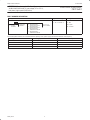
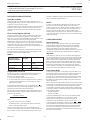
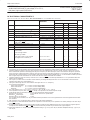
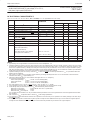
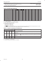
SELECTION TABLE
For applications requiring more ROM and RAM, as well as more
on-chip peripherals, see the P89C66x and P89C51Rx2 data sheets.
Type Memory Timers Serial Interfaces
RAM
ROM
OTP
Flash
# of Timers
PWM
PCA
WD
UART
I
2
C
CAN
SPI
ADC bits/ch.
I/O Pins
Interrupts
(External)
Program
Security
Default Clock
Rate
Optional
Clock Rate
Max.
Freq.
at 6-clk
/ 12-clk
(MHz)
Freq.
Range
at 3V
(MHz)
Freq.
Range
at 5V
(MHz)
P87C58X2
256B – 32K – 3 – – –
n
– – – – 32 6 (2)
n
12–clk 6-clk 30/33 0–16 0–30/33
P80C58X2
256B 32K – – 3 – – –
n
– – – – 32 6 (2)
n
12–clk 6-clk 30/33 0–16 0–30/33
P87C54X2
256B – 16K – 3 – – –
n
– – – – 32 6 (2)
n
12–clk 6-clk 30/33 0–16 0–30/33
P80C54X2
256B 16K – – 3 – – –
n
– – – – 32 6 (2)
n
12–clk 6-clk 30/33 0–16 0–30/33
P87C52X2
256B – 8K – 3 – – –
n
– – – – 32 6 (2)
n
12–clk 6-clk 30/33 0–16 0–30/33
P80C52X2
256B 8K – – 3 – – –
n
– – – – 32 6 (2)
n
12–clk 6-clk 30/33 0–16 0–30/33
P87C51X2
128B – 4K – 3 – – –
n
– – – – 32 6 (2)
n
12–clk 6-clk 30/33 0–16 0–30/33
P80C51X2
128B 4K – – 3 – – –
n
– – – – 32 6 (2)
n
12–clk 6-clk 30/33 0–16 0–30/33
P80C32X2
256B – – – 3 – – –
n
– – – – 32 6 (2) – 12–clk 6-clk 30/33 0–16 0–30/33
P80C31X2
128B – – – 3 – – –
n
– – – – 32 6 (2) – 12–clk 6-clk 30/33 0–16 0–30/33
NOTE:
1. I
2
C = Inter-Integrated Circuit Bus; CAN = Controller Area Network; SPI = Serial Peripheral Interface; PCA = Programmable Counter Array;
ADC = Analog-to-Digital Converter; PWM = Pulse Width Modulation

Philips Semiconductors Product data
P80C3xX2; P80C5xX2;
P87C5xX2
80C51 8-bit microcontroller family
4K/8K/16K/32K ROM/OTP, low voltage (2.7 to 5.5 V),
low power, high speed (30/33 MHz)
2003 Jan 24
3
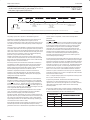
FEATURES
•80C51 Central Processing Unit
– 4 kbytes ROM/EPROM (P80/P87C51X2)
– 8 kbytes ROM/EPROM (P80/P87C52X2)
– 16 kbytes ROM/EPROM (P80/P87C54X2)
– 32 kbytes ROM/EPROM (P80/P87C58X2)
– 128 byte RAM (P80/P87C51X2 and P80C31X2)
– 256 byte RAM (P80/P87C52/54X2/58X2 and P80C32X2)
– Boolean processor
– Fully static operation
– Low voltage (2.7 V to 5.5 V at 16 MHz) operation
•12-clock operation with selectable 6-clock operation (via software
or via parallel programmer)
•Memory addressing capability
– Up to 64 kbytes ROM and 64 kbytes RAM
•Power control modes:
– Clock can be stopped and resumed
– Idle mode
– Power-down mode
•CMOS and TTL compatible
•Two speed ranges at V
CC
= 5 V
– 0 to 30 MHz with 6-clock operation
– 0 to 33 MHz with 12-clock operation
•PLCC, DIP, TSSOP or LQFP packages
•Extended temperature ranges
•Dual Data Pointers
•Security bits:
– ROM (2 bits)
– OTP (3 bits)
•Encryption array - 64 bytes
•Four interrupt priority levels
•Six interrupt sources
•Four 8-bit I/O ports
•Full-duplex enhanced UART
– Framing error detection
– Automatic address recognition
•Three 16-bit timers/counters T0, T1 (standard 80C51) and
additional T2 (capture and compare)
•Programmable clock-out pin
•Asynchronous port reset
•Low EMI (inhibit ALE, slew rate controlled outputs, and 6-clock
mode)
•Wake-up from Power Down by an external interrupt.

Philips Semiconductors Product data
P80C3xX2; P80C5xX2;
P87C5xX2
80C51 8-bit microcontroller family
4K/8K/16K/32K ROM/OTP, low voltage (2.7 to 5.5 V),
low power, high speed (30/33 MHz)
2003 Jan 24
4
P80C31/32X2 ORDERING INFORMATION (ROMLESS)
Type number Package Temperature
R(°C)
Name Description Version
Range (°C)
P80C31X2BA PLCC44 plastic leaded chip carrier; 44 leads SOT187-2 0 to +70
P80C31X2BN DIP40 plastic dual in-line package; 40 leads (600 mil) SOT129-1 0 to +70
P80C32X2BA PLCC44 plastic leaded chip carrier; 44 leads SOT187-2 0 to +70
P80C32X2BN DIP40 plastic dual in-line package; 40 leads (600 mil) SOT129-1 0 to +70
P80C32X2BBD LQFP44 plastic low profile quad flat package; 44 leads; body 10 x 10 x 1.4 mm SOT389-1 0 to +70
P80C32X2FA PLCC44 plastic leaded chip carrier; 44 leads SOT187-2 –40 to +85
P80C32X2FN DIP40 plastic dual in-line package; 40 leads (600 mil) SOT129-1 –40 to +85
P87C51X2 ORDERING INFORMATION (4 KBYTE OTP)
Type number Package Temperature
R(°C)
Name Description Version
Range (°C)
P87C51X2BA PLCC44 plastic leaded chip carrier; 44 leads SOT187-2 0 to +70
P87C51X2BN DIP40 plastic dual in-line package; 40 leads (600 mil) SOT129-1 0 to +70
P87C51X2BBD LQFP44 plastic low profile quad flat package; 44 leads; body 10 x 10 x 1.4 mm SOT389-1 0 to +70
P87C51X2FA PLCC44 plastic leaded chip carrier; 44 leads SOT187-2 –40 to +85
P87C51X2FBD LQFP44 plastic low profile quad flat package; 44 leads; body 10 x 10 x 1.4 mm SOT389-1 –40 to +85
P87C52X2 ORDERING INFORMATION (8 KBYTE OTP)
Type number Package Temperature
R(°C)
Name Description Version
Range (°C)
P87C52X2BA PLCC44 plastic leaded chip carrier; 44 leads SOT187-2 0 to +70
P87C52X2BN DIP40 plastic dual in-line package; 40 leads (600 mil) SOT129-1 0 to +70
P87C52X2BBD LQFP44 plastic low profile quad flat package; 44 leads; body 10 x 10 x 1.4 mm SOT389-1 0 to +70
P87C52X2FA PLCC44 plastic leaded chip carrier; 44 leads SOT187-2 –40 to +85
P87C52X2FN DIP40 plastic dual in-line package; 40 leads (600 mil) SOT129-1 –40 to +85
P87C52X2FBD LQFP44 plastic low profile quad flat package; 44 leads; body 10 x 10 x 1.4 mm SOT389-1 –40 to +85
P87C54X2 ORDERING INFORMATION (16 KBYTE OTP)
Type number Package Temperature
R(°C)
Name Description Version
Range (°C)
P87C54X2BA PLCC44 plastic lead chip carrier; 44 leads SOT187-2 0 to +70
P87C54X2BN DIP40 plastic dual in-line package; 40 leads (600 mil) SOT129-1 0 to +70
P87C54X2BBD LQFP44 plastic low profile quad flat package; 44 leads; body 10 x 10 x 1.4 mm SOT389-1 0 to +70
P87C54X2BDH TSSOP38 plastic thin shrink small outline package; 38 leads; body width 4.4 mm;
lead pitch 0.5 mm
SOT510-1 0 to +70
P87C54X2FA PLCC44 plastic lead chip carrier; 44 leads SOT187-2 –40 to +85
P87C54X2FBD LQFP44 plastic low profile quad flat package; 44 leads; body 10 x 10 x 1.4 mm SOT389-1 –40 to +85
P87C58X2 ORDERING INFORMATION (32 KBYTE OTP)
Type number Package Temperature
R(°C)
Name Description Version
Range (°C)
P87C58X2BA PLCC44 plastic lead chip carrier; 44 leads SOT187-2 0 to +70
P87C58X2BN DIP40 plastic dual in-line package; 40 leads (600 mil) SOT129-1 0 to +70
P87C58X2BBD LQFP44 plastic low profile quad flat package; 44 leads; body 10 x 10 x 1.4 mm SOT389-1 0 to +70
P87C58X2FA PLCC44 plastic lead chip carrier; 44 leads SOT187-2 –40 to +85
P87C58X2FBD LQFP44 plastic low profile quad flat package; 44 leads; body 10 x 10 x 1.4 mm SOT389-1 –40 to +85
P87C58X2FN DIP40 plastic dual in-line package; 40 leads (600 mil) SOT129-1 –40 to +85
All OTP parts listed here are also available as ROM parts (80C5xX2). Please contact your Philips representative if you would like to order a
ROM part.

Philips Semiconductors Product data
P80C3xX2; P80C5xX2;
P87C5xX2
80C51 8-bit microcontroller family
4K/8K/16K/32K ROM/OTP, low voltage (2.7 to 5.5 V),
low power, high speed (30/33 MHz)
2003 Jan 24
5
PART NUMBER DERIVATION
Memory Temperature Range Package
P87C51X2
7 = OTP
0 = ROM or
ROMless
5 = ROM/OTP
3 = ROMless
1 = 128 BYTES RAM
4 KBYTES ROM/OTP
2 = 256 BYTES RAM
8 KBYTES ROM/OTP
4 = 256 BYTES RAM
16 KBYTES ROM/OTP
8 = 256 BYTES RAM
32 KBYTES ROM/OTP
X2 = 6-clock
mode available
B = 0 °C TO +70 °C
F = –40 °C TO +85 °C
A = PLCC
N = DIP
BD = LQFP
DH = TSSOP
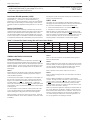
The following table illustrates the correlation between operating mode, power supply and maximum external clock frequency:
Operating Mode
Power Supply Maximum Clock Frequency
6-clock 5 V ± 10% 30 MHz
6-clock 2.7 V to 5.5 V 16 MHz
12-clock 5 V ± 10% 33 MHz
12-clock 2.7 V to 5.5 V 16 MHz

Philips Semiconductors Product data
P80C3xX2; P80C5xX2;
P87C5xX2
80C51 8-bit microcontroller family
4K/8K/16K/32K ROM/OTP, low voltage (2.7 to 5.5 V),
low power, high speed (30/33 MHz)
2003 Jan 24
6
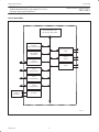
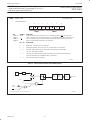
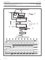
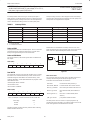
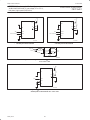
BLOCK DIAGRAM 1
su01579
Accelerated 80C51 CPU
(12-clk mode, 6-clk mode)
0K / 4K / 8K / 16K /
32 kbyte
CODE ROM / EPROM
128 / 256 Byte
Data RAM
Port 3
Configurable I/Os
Port 2
Configurable I/Os
Port 1
Configurable I/Os
Port 0
Configurable I/Os
OscillatorCrystal or
Resonator
Full-duplex enhanced
UART
Timer 0
Timer 1
Timer 2

Philips Semiconductors Product data
P80C3xX2; P80C5xX2;
P87C5xX2
80C51 8-bit microcontroller family
4K/8K/16K/32K ROM/OTP, low voltage (2.7 to 5.5 V),
low power, high speed (30/33 MHz)
2003 Jan 24
7
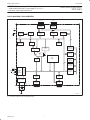
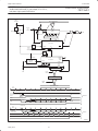
BLOCK DIAGRAM 2 (CPU-ORIENTED)
su01723
PSEN
EA / V
PP
ALE/PROG
RST
XTAL1 XTAL2
V
CC
V
SS
PORT 0
DRIVERS
PORT 2
DRIVERS
RAM ADDR
REGISTER
RAM
PORT 0
LATCH
PORT 2
LATCH
ROM/EPROM
REGISTER
B
ACC
STACK
POINTER
TMP2
TMP1
ALU
TIMING
AND
CONTROL
INSTRUCTION
REGISTER
PD
OSCILLATOR
PSW
PORT 1
LATCH
PORT 3
LATCH
PORT 1
DRIVERS
PORT 3
DRIVERS
PROGRAM
ADDRESS
REGISTER
BUFFER
PC
INCRE-
MENTER
PROGRAM
COUNTER
DPTR’S
MULTIPLE
P1.0–P1.7
P3.0–P3.7
1
P0.0–P0.7 P2.0–P2.7
SFRs
TIMERS
8
8 16
NOTE:
1. P3.2 and P3.5 absent in the TSSOP38 package.

Philips Semiconductors Product data
P80C3xX2; P80C5xX2;
P87C5xX2
80C51 8-bit microcontroller family
4K/8K/16K/32K ROM/OTP, low voltage (2.7 to 5.5 V),
low power, high speed (30/33 MHz)
2003 Jan 24
8
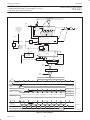
LOGIC SYMBOL
PORT 0
PORT 1PORT 2
PORT 3
ADDRESS AND
DATA BUS
ADDRESS BUS
T2
T2EX
RxD
TxD
INT0
1
INT1
T0
T1
1
WR
RD
SECONDARY FUNCTIONS
RST
EA/V
PP
PSEN
ALE/PROG
V
SS
V
CC
XTAL1
XTAL2
SU01724
NOTE:
1. INT0
/P3.2 and T1/P3.5 are absent in the TSSOP38 package.
PLASTIC DUAL IN-LINE PACKAGE
PIN CONFIGURATIONS
SU01063
1
2
3
4
5
6
7
8
9
10
11
12
13
14
15
16
17
18
19
20
21
22
23
24
25
26
27
28
29
30
31
32
33
34
35
36
37
38
39
40
T2/P1.0
T2EX/P1.1
P1.2
P1.3
P1.4
P1.5
P1.6
RST
RxD/P3.0
TxD/P3.1
INT0
/P3.2
INT1
/P3.3
T0/P3.4
T1/P3.5
P1.7
WR
/P3.6
RD
/P3.7
XTAL2
XTAL1
V
SS
P2.0/A8
P2.1/A9
P2.2/A10
P2.3/A11
P2.4/A12
P2.5/A13
P2.6/A14
P2.7/A15
PSEN
ALE
EA
/V
PP
P0.7/AD7
P0.6/AD6
P0.5/AD5
P0.4/AD4
P0.3/AD3
P0.2/AD2
P0.1/AD1
P0.0/AD0
V
CC
DUAL
IN-LINE
PACKAGE

Philips Semiconductors Product data
P80C3xX2; P80C5xX2;
P87C5xX2
80C51 8-bit microcontroller family
4K/8K/16K/32K ROM/OTP, low voltage (2.7 to 5.5 V),
low power, high speed (30/33 MHz)
2003 Jan 24
9
PLASTIC LEADED CHIP CARRIER PIN FUNCTIONS
SU01062
PLCC
6140
7
17
39
29
18 28
Pin Function
1 NIC*
2 P1.0/T2
3 P1.1/T2EX
4 P1.2
5 P1.3
6 P1.4
7 P1.5
8 P1.6
9 P1.7
10 RST
11 P3.0/RxD
12 NIC*
13 P3.1/TxD
14 P3.2/INT0
15 P3.3/INT1
Pin Function
16 P3.4/T0
17 P3.5/T1
18 P3.6/WR
19 P3.7/RD
20 XTAL2
21 XTAL1
22 V
SS
23 NIC*
24 P2.0/A8
25 P2.1/A9
26 P2.2/A10
27 P2.3/A11
28 P2.4/A12
29 P2.5/A13
30 P2.6/A14
Pin Function
31 P2.7/A15
32 PSEN
33 ALE
34 NIC*
35 EA/V
PP
36 P0.7/AD7
37 P0.6/AD6
38 P0.5/AD5
39 P0.4/AD4
40 P0.3/AD3
41 P0.2/AD2
42 P0.1/AD1
43 P0.0/AD0
44 V
CC
* NO INTERNAL CONNECTION
LOW PROFILE QUAD FLAT PACK
PIN FUNCTIONS
SU01487
LQFP
44 34
1
11
33
23
12 22
Pin Function
1 P1.5
2 P1.6
3 P1.7
4 RST
5 P3.0/RxD
6 NIC*
7 P3.1/TxD
8 P3.2/INT0
9 P3.3/INT1
10 P3.4/T0
11 P3.5/T1
12 P3.6/WR
13 P3.7/RD
14 XTAL2
15 XTAL1
Pin Function
16 V
SS
17 NIC*
18 P2.0/A8
19 P2.1/A9
20 P2.2/A10
21 P2.3/A11
22 P2.4/A12
23 P2.5/A13
24 P2.6/A14
25 P2.7/A15
26 PSEN
27 ALE
28 NIC*
29 EA
/V
PP
30 P0.7/AD7
Pin Function
31 P0.6/AD6
32 P0.5/AD5
33 P0.4/AD4
34 P0.3/AD3
35 P0.2/AD2
36 P0.1/AD1
37 P0.0/AD0
38 V
CC
39 NIC*
40 P1.0/T2
41 P1.1/T2EX
42 P1.2
43 P1.3
44 P1.4
* NO INTERNAL CONNECTION
PLASTIC THIN SHRINK SMALL OUTLINE PACK
PIN FUNCTIONS
su01725
Pin Function
1 P3.0/RxD
2 P3.1/TxD
3 P3.3/INT1
4 P3.4/T0
5 P3.6/WR
6 P3.7/RD
7 XTAL2
8 XTAL1
9V
SS
10 P2.0/A8
11 P2.1/A9
12 P2.2/A10
13 P2.3/A11
Pin Function
14 P2.4/A12
15 P2.5/A13
16 P2.6/A14
17 P2.7/A15
18 PSEN
19 ALE/PROG
20 EA/V
PP
21 P0.7/AD7
22 P0.6/AD6
23 P0.5/AD5
24 P0.4/AD4
25 P0.3/AD3
26 P0.2/AD2
Pin Function
27 P0.1/AD1
28 P0.0/AD0
29 V
DD
30 P1.0/T2
31 P1.1/T2EX
32 P1.2
33 P1.3
34 P1.4
35 P1.5
36 P1.6
37 P1.7
38 RST
1
19 20
38
TSSOP

Philips Semiconductors Product data
P80C3xX2; P80C5xX2;
P87C5xX2
80C51 8-bit microcontroller family
4K/8K/16K/32K ROM/OTP, low voltage (2.7 to 5.5 V),
low power, high speed (30/33 MHz)
2003 Jan 24
10
PIN DESCRIPTIONS
PIN NUMBER
MNEMONIC DIP PLCC LQFP TSSOP TYPE NAME AND FUNCTION
V
SS
20 22 16 9 I Ground: 0 V reference.
V
CC
40 44 38 29 I Power Supply: This is the power supply voltage for normal, idle, and power-down
operation.
P0.0-0.7 39–32 43–36 37–30 28–21 I/O Port 0: Port 0 is an open-drain, bidirectional I/O port. Port 0 pins that have 1s
written to them float and can be used as high-impedance inputs. Port 0 is also the
multiplexed low-order address and data bus during accesses to external program
and data memory. In this application, it uses strong internal pull-ups when emitting
1s. Port 0 also outputs the code bytes during program verification and received
code bytes during EPROM programming. External pull-ups are required during
program verification.
P1.0–P1.7 1–8 2–9 40–44,
1–3
30–37 I/O Port 1: Port 1 is an 8-bit bidirectional I/O port with internal pull-ups. Port 1 pins that
have 1s written to them are pulled high by the internal pull-ups and can be used as
inputs. As inputs, port 1 pins that are externally pulled low will source current
because of the internal pull-ups. (See DC Electrical Characteristics: I
IL
). Port 1 also
receives the low-order address byte during program memory verification. Alternate
functions for Port 1 include:
1 2 40 30 I/O T2 (P1.0): Timer/Counter 2 external count input/clockout (see Programmable
Clock-Out)
2 3 41 31 I T2EX (P1.1): Timer/Counter 2 Reload/Capture/Direction control
P2.0–P2.7 21–28 24–31 18–25 10–17 I/O Port 2: Port 2 is an 8-bit bidirectional I/O port with internal pull-ups. Port 2 pins that
have 1s written to them are pulled high by the internal pull-ups and can be used as
inputs. As inputs, port 2 pins that are externally being pulled low will source current
because of the internal pull-ups. (See DC Electrical Characteristics: I
IL
). Port 2
emits the high-order address byte during fetches from external program memory
and during accesses to external data memory that use 16-bit addresses (MOVX
@DPTR). In this application, it uses strong internal pull-ups when emitting 1s.
During accesses to external data memory that use 8-bit addresses (MOV @Ri), port
2 emits the contents of the P2 special function register. Some Port 2 pins receive
the high order address bits during EPROM programming and verification.
P3.0–P3.7 10–17 11,
13–19
5,
7–13
1–6 I/O Port 3: Port 3 is an 8-bit bidirectional I/O port with internal pull-ups. Port 3 pins that
have 1s written to them are pulled high by the internal pull-ups and can be used as
inputs. As inputs, port 3 pins that are externally being pulled low will source current
because of the pull-ups. (See DC Electrical Characteristics: I
IL
). Port 3 also serves
the special features of the 80C51 family, as listed below:
10 11 5 1 I RxD (P3.0): Serial input port
11 13 7 2 O TxD (P3.1): Serial output port
12 14 8 I INT0 (P3.2): External interrupt
1
13 15 9 3 I INT1 (P3.3): External interrupt
14 16 10 4 I T0 (P3.4): Timer 0 external input
15 17 11 I T1 (P3.5): Timer 1 external input
1
16 18 12 5 O WR (P3.6): External data memory write strobe
17 19 13 6 O RD (P3.7): External data memory read strobe
RST 9 10 4 38 I Reset: A high on this pin for two machine cycles while the oscillator is running,
resets the device. An internal diffused resistor to V
SS
permits a power-on reset
using only an external capacitor to V
CC
.
ALE/PROG 30 33 27 19 O Address Latch Enable/Program Pulse: Output pulse for latching the low byte of
the address during an access to external memory. In normal operation, ALE is
emitted at a constant rate of 1/6 (12-clock Mode) or 1/3 (6-clock Mode) the
oscillator frequency, and can be used for external timing or clocking. Note that one
ALE pulse is skipped during each access to external data memory. This pin is also
the program pulse input (PROG) during EPROM programming. ALE can be
disabled by setting SFR auxiliary.0. With this bit set, ALE will be active only during
a MOVX instruction.

Philips Semiconductors Product data
P80C3xX2; P80C5xX2;
P87C5xX2
80C51 8-bit microcontroller family
4K/8K/16K/32K ROM/OTP, low voltage (2.7 to 5.5 V),
low power, high speed (30/33 MHz)
2003 Jan 24
11
PIN NUMBER
MNEMONIC NAME AND FUNCTIONTYPETSSOPLQFPPLCCDIP
PSEN 29 32 26 18 O Program Store Enable: The read strobe to external program memory. When the
device is executing code from the external program memory, PSEN is activated
twice each machine cycle, except that two PSEN activations are skipped during
each access to external data memory. PSEN is not activated during fetches from
internal program memory.
EA/V
PP
31 35 29 20 I External Access Enable/Programming Supply Voltage: EA must be externally held low to enable
the device to fetch code from external program memory locations 0000H to
0FFFH/1FFFH/3FFFH/7FFFH. If EA is held high, the device executes from internal program memory
unless the program counter contains an address greater than the on-chip ROM/OTP. This pin also
receives the 12.75 V programming supply voltage (V
PP
) during EPROM programming. If security bit
1 is programmed, EA will be internally latched on Reset.
XTAL1 19 21 15 8 I Crystal 1: Input to the inverting oscillator amplifier and input to the internal clock
generator circuits.
XTAL2 18 20 14 7 O Crystal 2: Output from the inverting oscillator amplifier.
NOTES:
To avoid “latch-up” effect at power-on, the voltage on any pin at any time must not be higher than V
CC
+ 0.5 V or V
SS
– 0.5 V, respectively.
1. Absent in the TSSOP38 package.

Philips Semiconductors Product data
P80C3xX2; P80C5xX2;
P87C5xX2
80C51 8-bit microcontroller family
4K/8K/16K/32K ROM/OTP, low voltage (2.7 to 5.5 V),
low power, high speed (30/33 MHz)
2003 Jan 24
12
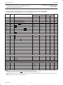
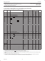
Table 1. Special Function Registers
SYMBOL DESCRIPTION
DIRECT
ADDRESS
BIT ADDRESS, SYMBOL, OR ALTERNATIVE PORT FUNCTION
MSB LSB
RESET
VALUE
ACC* Accumulator E0H
E7 E6 E5 E4 E3 E2 E1 E0
00H
AUXR# Auxiliary 8EH – – – – – – – AO xxxxxxx0B
AUXR1# Auxiliary 1 A2H – – – LPEP
2
WUPD 0 – DPS xxx000x0B
B* B register F0H
F7 F6 F5 F4 F3 F2 F1 F0
00H
CKCON Clock Control Register 8FH – – – – – – – X2 xxx00000B
DPTR: Data Pointer (2 bytes)
DPH Data Pointer High 83H 00H
DPL Data Pointer Low 82H 00H
AF AE AD AC AB AA A9 A8
IE* Interrupt Enable A8H EA – ET2 ES ET1 EX1 ET0 EX0 0x000000B
BF BE BD BC BB BA B9 B8
IP* Interrupt Priority B8H – – PT2 PS PT1 PX1 PT0 PX0 xx000000B
IPH# Interrupt Priority High B7H – – PT2H PSH PT1H PX1H PT0H PX0H xx000000B
87 86 85 84 83 82 81 80
P0* Port 0 80H AD7 AD6 AD5 AD4 AD3 AD2 AD1 AD0 FFH
97 96 95 94 93 92 91 90
P1* Port 1 90H – – – – – – T2EX T2 FFH
A7 A6 A5 A4 A3 A2 A1 A0
P2* Port 2 A0H AD15 AD14 AD13 AD12 AD11 AD10 AD9 AD8 FFH
B7 B6 B5 B4 B3 B2 B1 B0
P3* Port 3 B0H RD WR T1 T0 INT1 INT0 TxD RxD FFH
PCON#
1
Power Control 87H SMOD1 SMOD0 – POF GF1 GF0 PD IDL 00xx0000B
D7 D6 D5 D4 D3 D2 D1 D0
PSW* Program Status Word D0H CY AC F0 RS1 RS0 OV – P 000000x0B
RACAP2H# Timer 2 Capture High CBH 00H
RACAP2L# Timer 2 Capture Low CAH 00H
SADDR# Slave Address A9H 00H
SADEN# Slave Address Mask B9H 00H
SBUF Serial Data Buffer 99H xxxxxxxxB
9F 9E 9D 9C 9B 9A 99 98
SCON* Serial Control 98H
SM0/FE
SM1 SM2 REN TB8 RB8 TI RI 00H
SP Stack Pointer 81H 07H
8F 8E 8D 8C 8B 8A 89 88
TCON* Timer Control 88H TF1 TR1 TF0 TR0 IE1 IT1 IE0 IT0 00H
CF CE CD CC CB CA C9 C8
T2CON* Timer 2 Control C8H TF2 EXF2 RCLK TCLK EXEN2 TR2 C/T2 CP/RL2 00H
T2MOD# Timer 2 Mode Control C9H – – – – – – T2OE DCEN xxxxxx00B
TH0 Timer High 0 8CH 00H
TH1 Timer High 1 8DH 00H
TH2# Timer High 2 CDH 00H
TL0 Timer Low 0 8AH 00H
TL1 Timer Low 1 8BH 00H
TL2# Timer Low 2 CCH 00H
TMOD Timer Mode 89H GATE C/T M1 M0 GATE C/T M1 M0 00H
NOTE:
Unused register bits that are not defined should not be set by the user’s program. If violated, the device could function incorrectly.
* SFRs are bit addressable.
# SFRs are modified from or added to the 80C51 SFRs.
– Reserved bits.
1. Reset value depends on reset source.
2. LPEP – Low Power EPROM operation (OTP only)

Philips Semiconductors Product data
P80C3xX2; P80C5xX2;
P87C5xX2
80C51 8-bit microcontroller family
4K/8K/16K/32K ROM/OTP, low voltage (2.7 to 5.5 V),
low power, high speed (30/33 MHz)
2003 Jan 24
13
OSCILLATOR CHARACTERISTICS
Using the oscillator
XTAL1 and XTAL2 are the input and output, respectively, of an
inverting amplifier. The pins can be configured for use as an on-chip
oscillator, as shown in the logic symbol.
To drive the device from an external clock source, XTAL1 should be
driven while XTAL2 is left unconnected. However, minimum and
maximum high and low times specified in the data sheet must be
observed.
Clock Control Register (CKCON)
This device provides control of the 6-clock/12-clock mode by both
an SFR bit (bit X2 in register CKCON and an OTP bit (bit OX2).
When X2 is 0, 12-clock mode is activated. By setting this bit to 1, the
system is switching to 6-clock mode. Having this option
implemented as SFR bit, it can be accessed anytime and changed
to either value. Changing X2 from 0 to 1 will result in executing user
code at twice the speed, since all system time intervals will be
divided by 2. Changing back from 6-clock to 12-clock mode will slow
down running code by a factor of 2.
The OTP clock control bit (OX2) activates the 6-clock mode when
programmed using a parallel programmer, superceding the X2 bit
(CKCON.0). Please also see Table 2 below.
Table 2.
OX2 clock mode bit
(can only be set by
parallel programmer)
X2 bit
(CKCON.0)
CPU clock mode
erased 0 12-clock mode
(default)
erased 1 6-clock mode
programmed X 6-clock mode
Programmable Clock-Out
A 50% duty cycle clock can be programmed to be output on P1.0.
This pin, besides being a regular I/O pin, has two alternate
functions. It can be programmed:
1. to input the external clock for Timer/Counter 2, or
2. to output a 50% duty cycle clock ranging from 61 Hz to 4 MHz at
a 16 MHz operating frequency in 12-clock mode (122 Hz to
8 MHz in 6-clock mode).
To configure the Timer/Counter 2 as a clock generator, bit C/T
2 (in
T2CON) must be cleared and bit T20E in T2MOD must be set. Bit
TR2 (T2CON.2) also must be set to start the timer.
The Clock-Out frequency depends on the oscillator frequency and
the reload value of Timer 2 capture registers (RCAP2H, RCAP2L)
as shown in this equation:
Oscillator Frequency
n (65536–RCAP2H,RCAP2L)
Where:
n = 2 in 6-clock mode, 4 in 12-clock mode.
(RCAP2H,RCAP2L) = the content of RCAP2H and RCAP2L
taken as a 16-bit unsigned integer.
In the Clock-Out mode Timer 2 roll-overs will not generate an
interrupt. This is similar to when it is used as a baud-rate generator.
It is possible to use Timer 2 as a baud-rate generator and a clock
generator simultaneously. Note, however, that the baud-rate and the
Clock-Out frequency will be the same.
RESET
A reset is accomplished by holding the RST pin HIGH for at least
two machine cycles (24 oscillator periods in 12-clock and 12
oscillator periods in 6-clock mode), while the oscillator is running. To
insure a reliable power-up reset, the RST pin must be high long
enough to allow the oscillator time to start up (normally a few
milliseconds) plus two machine cycles. After the reset, the part runs
in 12-clock mode, unless it has been set to 6-clock operation using a
parallel programmer.
LOW POWER MODES
Stop Clock Mode
The static design enables the clock speed to be reduced down to
0 MHz (stopped). When the oscillator is stopped, the RAM and
Special Function Registers retain their values. This mode allows
step-by-step utilization and permits reduced system power
consumption by lowering the clock frequency down to any value. For
lowest power consumption the Power Down mode is suggested.
Idle Mode
In idle mode (see Table 3), the CPU puts itself to sleep while all of
the on-chip peripherals stay active. The instruction to invoke the idle
mode is the last instruction executed in the normal operating mode
before the idle mode is activated. The CPU contents, the on-chip
RAM, and all of the special function registers remain intact during
this mode. The idle mode can be terminated either by any enabled
interrupt (at which time the process is picked up at the interrupt
service routine and continued), or by a hardware reset which starts
the processor in the same manner as a power-on reset.
Power-Down Mode
To save even more power, a Power Down mode (see Table 3) can
be invoked by software. In this mode, the oscillator is stopped and
the instruction that invoked Power Down is the last instruction
executed. The on-chip RAM and Special Function Registers retain
their values down to 2.0 V and care must be taken to return V
CC
to
the minimum specified operating voltages before the Power Down
Mode is terminated.
Either a hardware reset or external interrupt can be used to exit from
Power Down. Reset redefines all the SFRs but does not change the
on-chip RAM. An external interrupt allows both the SFRs and the
on-chip RAM to retain their values. WUPD (AUXR1.3–Wakeup from
Power Down) enables or disables the wakeup from power down with
external interrupt. Where:
WUPD = 0: Disable
WUPD = 1: Enable
To properly terminate Power Down, the reset or external interrupt
should not be executed before V
CC
is restored to its normal
operating level and must be held active long enough for the
oscillator to restart and stabilize (normally less than 10 ms).
To terminate Power Down with an external interrupt, INT0
or INT1
must be enabled and configured as level-sensitive. Holding the pin
low restarts the oscillator but bringing the pin back high completes
the exit. Once the interrupt is serviced, the next instruction to be
executed after RETI will be the one following the instruction that put
the device into Power Down.

Philips Semiconductors Product data
P80C3xX2; P80C5xX2;
P87C5xX2
80C51 8-bit microcontroller family
4K/8K/16K/32K ROM/OTP, low voltage (2.7 to 5.5 V),
low power, high speed (30/33 MHz)
2003 Jan 24
14
Low-Power EPROM operation (LPEP)
The EPROM array contains some analog circuits that are not
required when V
CC
is less than 4 V, but are required for a V
CC
greater than 4 V. The LPEP bit (AUXR.4), when set, will powerdown
these analog circuits resulting in a reduced supply current. This bit
should be set ONLY for applications that operate at a V
CC
less than
4 V.
Design Consideration
When the idle mode is terminated by a hardware reset, the device
normally resumes program execution from where it left off, up to two
machine cycles before the internal reset algorithm takes control.
On-chip hardware inhibits access to internal RAM in this event, but
access to the port pins is not inhibited. To eliminate the possibility of
an unexpected write when Idle is terminated by reset, the instruction
following the one that invokes Idle should not be one that writes to a
port pin or to external memory.
ONCE Mode
The ONCE (“On-Circuit Emulation”) Mode facilitates testing and
debugging of systems without the device having to be removed from
the circuit. The ONCE Mode is invoked in the following way:
1. Pull ALE low while the device is in reset and PSEN
is high;
2. Hold ALE low as RST is deactivated.
While the device is in ONCE Mode, the Port 0 pins go into a float
state, and the other port pins and ALE and PSEN
are weakly pulled
high. The oscillator circuit remains active. While the device is in this
mode, an emulator or test CPU can be used to drive the circuit.
Normal operation is restored when a normal reset is applied.
Table 3. External Pin Status During Idle and Power-Down Modes
MODE PROGRAM MEMORY ALE PSEN PORT 0 PORT 1 PORT 2 PORT 3
Idle Internal 1 1 Data Data Data Data
Idle External 1 1 Float Data Address Data
Power-down Internal 0 0 Data Data Data Data
Power-down External 0 0 Float Data Data Data
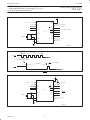
TIMER 0 AND TIMER 1 OPERATION
Timer 0 and Timer 1
The “Timer” or “Counter” function is selected by control bits C/T in
the Special Function Register TMOD. These two Timer/Counters
have four operating modes, which are selected by bit-pairs (M1, M0)
in TMOD. Modes 0, 1, and 2 are the same for both Timers/Counters.
Mode 3 is different. The four operating modes are described in the
following text.
Mode 0
Putting either Timer into Mode 0 makes it look like an 8048 Timer,
which is an 8-bit Counter with a divide-by-32 prescaler. Figure 2
shows the Mode 0 operation.
In this mode, the Timer register is configured as a 13-bit register. As
the count rolls over from all 1s to all 0s, it sets the Timer interrupt
flag TFn. The counted input is enabled to the Timer when TRn = 1
and either GATE = 0 or INTn
= 1. (Setting GATE = 1 allows the
Timer to be controlled by external input INTn
, to facilitate pulse width
measurements). TRn is a control bit in the Special Function Register
TCON (Figure 3).
The 13-bit register consists of all 8 bits of THn and the lower 5 bits
of TLn. The upper 3 bits of TLn are indeterminate and should be
ignored. Setting the run flag (TRn) does not clear the registers.
Mode 0 operation is the same for Timer 0 as for Timer 1. There are
two different GATE bits, one for Timer 1 (TMOD.7) and one for Timer
0 (TMOD.3).
Mode 1
Mode 1 is the same as Mode 0, except that the Timer register is
being run with all 16 bits.
Mode 2
Mode 2 configures the Timer register as an 8-bit Counter (TLn) with
automatic reload, as shown in Figure 4. Overflow from TLn not only
sets TFn, but also reloads TLn with the contents of THn, which is
preset by software. The reload leaves THn unchanged.
Mode 2 operation is the same for Timer 0 as for Timer 1.
Mode 3
Timer 1 in Mode 3 simply holds its count. The effect is the same as
setting TR1 = 0.
Timer 0 in Mode 3 establishes TL0 and TH0 as two separate
counters. The logic for Mode 3 on Timer 0 is shown in Figure 5. TL0
uses the Timer 0 control bits: C/T
, GATE, TR0, and TF0 as well as
pin INT0
. TH0 is locked into a timer function (counting machine
cycles) and takes over the use of TR1 and TF1 from Timer 1. Thus,
TH0 now controls the “Timer 1” interrupt.
Mode 3 is provided for applications requiring an extra 8-bit timer on
the counter. With Timer 0 in Mode 3, an 80C51 can look like it has
three Timer/Counters. When Timer 0 is in Mode 3, Timer 1 can be
turned on and off by switching it out of and into its own Mode 3, or
can still be used by the serial port as a baud rate generator, or in
fact, in any application not requiring an interrupt.

Philips Semiconductors Product data
P80C3xX2; P80C5xX2;
P87C5xX2
80C51 8-bit microcontroller family
4K/8K/16K/32K ROM/OTP, low voltage (2.7 to 5.5 V),
low power, high speed (30/33 MHz)
2003 Jan 24
15
GATE C/T M1
M0 GATE C/T
M1 M0
BIT SYMBOL FUNCTION
TMOD.3/ GATE Gating control when set. Timer/Counter “n” is enabled only while “INTn
” pin is high and
TMOD.7 “TRn” control pin is set. when cleared Timer “n” is enabled whenever “TRn” control bit is set.
TMOD.2/ C/T
Timer or Counter Selector cleared for Timer operation (input from internal system clock.)
TMOD.6 Set for Counter operation (input from “Tn” input pin).
M1 M0 OPERATING
0 0 8048 Timer: “TLn” serves as 5-bit prescaler.
0 1 16-bit Timer/Counter: “THn” and “TLn” are cascaded; there is no prescaler.
1 0 8-bit auto-reload Timer/Counter: “THn” holds a value which is to be reloaded
into “TLn” each time it overflows.
1 1 (Timer 0) TL0 is an 8-bit Timer/Counter controlled by the standard Timer 0 control bits.
TH0 is an 8-bit timer only controlled by Timer 1 control bits.
1 1 (Timer 1) Timer/Counter 1 stopped.
SU01580
TIMER 1 TIMER 0
Not Bit Addressable
TMOD Address = 89H Reset Value = 00H
76543 2 1 0
Figure 1. Timer/Counter 0/1 Mode Control (TMOD) Register
INTn Pin
Timer n
Gate bit
TRn
TLn
(5 Bits)
THn
(8 Bits)
TFn Interrupt
Control
C/T = 0
C/T = 1
SU01618
OSC
÷ d*
Tn Pin
*d = 6 in 6-clock mode; d = 12 in 12-clock mode.
Figure 2. Timer/Counter 0/1 Mode 0: 13-Bit Timer/Counter

Philips Semiconductors Product data
P80C3xX2; P80C5xX2;
P87C5xX2
80C51 8-bit microcontroller family
4K/8K/16K/32K ROM/OTP, low voltage (2.7 to 5.5 V),
low power, high speed (30/33 MHz)
2003 Jan 24
16
IT0
BIT SYMBOL FUNCTION
TCON.7 TF1 Timer 1 overflow flag. Set by hardware on Timer/Counter overflow.
Cleared by hardware when processor vectors to interrupt routine, or clearing the bit in software.
TCON.6 TR1 Timer 1 Run control bit. Set/cleared by software to turn Timer/Counter on/off.
TCON.5 TF0 Timer 0 overflow flag. Set by hardware on Timer/Counter overflow.
Cleared by hardware when processor vectors to interrupt routine, or by clearing the bit in software.
TCON.4 TR0 Timer 0 Run control bit. Set/cleared by software to turn Timer/Counter on/off.
TCON.3 IE1 Interrupt 1 Edge flag. Set by hardware when external interrupt edge detected.
Cleared when interrupt processed.
TCON.2 IT1 Interrupt 1 type control bit. Set/cleared by software to specify falling edge/low level triggered
external interrupts.
TCON.1 IE0 Interrupt 0 Edge flag. Set by hardware when external interrupt edge detected.
Cleared when interrupt processed.
TCON.0 IT0 Interrupt 0 Type control bit. Set/cleared by software to specify falling edge/low level
triggered external interrupts.
SU01516
IE0IT1IE1TR0TF0TR1TF1
Bit Addressable
TCON Address = 88H Reset Value = 00H
76543210
Figure 3. Timer/Counter 0/1 Control (TCON) Register
TLn
(8 Bits)
TFn
Interrupt
Control
C/T = 0
C/T
= 1
THn
(8 Bits)
Reload
INTn Pin
Timer n
Gate bit
TRn
SU01619
OSC
÷ d*
Tn Pin
*d = 6 in 6-clock mode; d = 12 in 12-clock mode.
Figure 4. Timer/Counter 0/1 Mode 2: 8-Bit Auto-Reload

Philips Semiconductors Product data
P80C3xX2; P80C5xX2;
P87C5xX2
80C51 8-bit microcontroller family
4K/8K/16K/32K ROM/OTP, low voltage (2.7 to 5.5 V),
low power, high speed (30/33 MHz)
2003 Jan 24
17
TL0
(8 Bits)
TF0
Interrupt
Control
TH0
(8 Bits)
TF1
Interrupt
Control
TR1
INT0 Pin
Timer 0
Gate bit
TR0
SU01620
C/T = 0
C/T
= 1
*d = 6 in 6-clock mode; d = 12 in 12-clock mode.
OSC
÷ d*
OSC
÷ d*
T0 Pin
Figure 5. Timer/Counter 0 Mode 3: Two 8-Bit Counters
TIMER 2 OPERATION
Timer 2
Timer 2 is a 16-bit Timer/Counter which can operate as either an
event timer or an event counter, as selected by C/T
2 in the special
function register T2CON (see Figure 6). Timer 2 has three operating
modes: Capture, Auto-reload (up or down counting), and Baud Rate
Generator, which are selected by bits in the T2CON as shown in
Table 4.
Capture Mode
In the capture mode there are two options which are selected by bit
EXEN2 in T2CON. If EXEN2=0, then timer 2 is a 16-bit timer or
counter (as selected by C/T
2 in T2CON) which, upon overflowing,
sets bit TF2, the timer 2 overflow bit. This bit can be used to
generate an interrupt (by enabling the Timer 2 interrupt bit in the
IE register). If EXEN2=1, Timer 2 operates as described above, but
with the added feature that a 1-to-0 transition at external input T2EX
causes the current value in the Timer 2 registers, TL2 and TH2, to
be captured into registers RCAP2L and RCAP2H, respectively. In
addition, the transition at T2EX causes bit EXF2 in T2CON to be
set, and EXF2 (like TF2) can generate an interrupt (which vectors to
the same location as Timer 2 overflow interrupt. The Timer 2
interrupt service routine can interrogate TF2 and EXF2 to determine
which event caused the interrupt). The capture mode is illustrated in
Figure 7 (There is no reload value for TL2 and TH2 in this mode.
Even when a capture event occurs from T2EX, the counter keeps on
counting T2EX pin transitions or osc/12 (12-clock Mode) or osc/6
(6-clock Mode) pulses).
Auto-Reload Mode (Up or Down Counter)
In the 16-bit auto-reload mode, Timer 2 can be configured as either
a timer or counter (C/T
2 in T2CON), then programmed to count up
or down. The counting direction is determined by bit DCEN (Down
Counter Enable) which is located in the T2MOD register (see
Figure 8). After reset, DCEN=0 which means Timer 2 will default to
counting up. If DCEN is set, Timer 2 can count up or down
depending on the value of the T2EX pin.
Figure 9 shows Timer 2 which will count up automatically since
DCEN=0. In this mode there are two options selected by bit EXEN2
in T2CON register. If EXEN2=0, then Timer 2 counts up to 0FFFFH
and sets the TF2 (Overflow Flag) bit upon overflow. This causes the
Timer 2 registers to be reloaded with the 16-bit value in RCAP2L
and RCAP2H. The values in RCAP2L and RCAP2H are preset by
software.
If EXEN2=1, then a 16-bit reload can be triggered either by an
overflow or by a 1-to-0 transition at input T2EX. This transition also
sets the EXF2 bit. The Timer 2 interrupt, if enabled, can be
generated when either TF2 or EXF2 are 1.
In Figure 10 DCEN=1 which enables Timer 2 to count up or down.
This mode allows pin T2EX to control the direction of count. When a
logic 1 is applied at pin T2EX, Timer 2 will count up. Timer 2 will
overflow at 0FFFFH and set the TF2 flag, which can then generate
an interrupt, if the interrupt is enabled. This timer overflow also
causes the 16-bit value in RCAP2L and RCAP2H to be reloaded
into the timer registers TL2 and TH2.
A logic 0 applied to pin T2EX causes Timer 2 to count down. The
timer will underflow when TL2 and TH2 become equal to the value
stored in RCAP2L and RCAP2H. A Timer 2 underflow sets the TF2
flag and causes 0FFFFH to be reloaded into the timer registers TL2
and TH2.
The external flag EXF2 toggles when Timer 2 underflows or
overflows. This EXF2 bit can be used as a 17th bit of resolution if
needed. The EXF2 flag does not generate an interrupt in this mode
of operation.

Philips Semiconductors Product data
P80C3xX2; P80C5xX2;
P87C5xX2
80C51 8-bit microcontroller family
4K/8K/16K/32K ROM/OTP, low voltage (2.7 to 5.5 V),
low power, high speed (30/33 MHz)
2003 Jan 24
18
Table 4. Timer 2 Operating Modes
RCLK + TCLK CP/RL2 TR2 MODE
0 0 1 16-bit Auto-reload
0 1 1 16-bit Capture
1 X 1 Baud rate generator
X X 0 (off)
Symbol Position Name and Significance
TF2 T2CON.7 Timer 2 overflow flag set by a Timer 2 overflow and must be cleared by software. TF2 will not be set
when either RCLK or TCLK = 1.
EXF2 T2CON.6 Timer 2 external flag set when either a capture or reload is caused by a negative transition on T2EX and
EXEN2 = 1. When Timer 2 interrupt is enabled, EXF2 = 1 will cause the CPU to vector to the Timer 2
interrupt routine. EXF2 must be cleared by software. EXF2 does not cause an interrupt in up/down
counter mode (DCEN = 1).
RCLK T2CON.5 Receive clock flag. When set, causes the serial port to use Timer 2 overflow pulses for its receive clock
in modes 1 and 3. RCLK = 0 causes Timer 1 overflow to be used for the receive clock.
TCLK T2CON.4 Transmit clock flag. When set, causes the serial port to use Timer 2 overflow pulses for its transmit clock
in modes 1 and 3. TCLK = 0 causes Timer 1 overflows to be used for the transmit clock.
EXEN2 T2CON.3 Timer 2 external enable flag. When set, allows a capture or reload to occur as a result of a negative
transition on T2EX if Timer 2 is not being used to clock the serial port. EXEN2 = 0 causes Timer 2 to
ignore events at T2EX.
TR2 T2CON.2 Start/stop control for Timer 2. A logic 1 starts the timer.
C/T
2 T2CON.1 Timer or counter select. (Timer 2)
0 = Internal timer (OSC/12 in 12-clock mode or OSC/6 in 6-clock mode)
1 = External event counter (falling edge triggered).
CP/RL
2 T2CON.0 Capture/Reload flag. When set, captures will occur on negative transitions at T2EX if EXEN2 = 1. When
cleared, auto-reloads will occur either with Timer 2 overflows or negative transitions at T2EX when
EXEN2 = 1. When either RCLK = 1 or TCLK = 1, this bit is ignored and the timer is forced to auto-reload
on Timer 2 overflow.
TF2 EXF2 RCLK TCLK EXEN2 TR2 C/T
2 CP/RL2
SU01621
Bit Addressable
T2CON Address = C8H Reset Value = 00H
76543210
Figure 6. Timer/Counter 2 (T2CON) Control Register

Philips Semiconductors Product data
P80C3xX2; P80C5xX2;
P87C5xX2
80C51 8-bit microcontroller family
4K/8K/16K/32K ROM/OTP, low voltage (2.7 to 5.5 V),
low power, high speed (30/33 MHz)
2003 Jan 24
19
TR2
Control
TL2
(8 bits)
TH2
(8 bits)
TF2
RCAP2L RCAP2H
EXEN2
Control
EXF2
Timer 2
Interrupt
T2EX Pin
Transition
Detector
Capture
SU01622
C/T2 = 0
C/T
2 = 1
*n = 6 in 6-clock mode; n = 12 in 12-clock mode.
OSC
÷ n*
T2 Pin
Figure 7. Timer 2 in Capture Mode
Not Bit Addressable
Symbol Position Function
— Not implemented, reserved for future use.*
T2OE T2MOD.1 Timer 2 Output Enable bit.
DCEN T2MOD.0 Down Count Enable bit. When set, this allows Timer 2 to be configured as an up/down
counter.
— — — — — — T2OE DCEN
SU01519
76543210
* User software should not write 1s to reserved bits. These bits may be used in future 8051 family products to invoke new features.
In that case, the reset or inactive value of the new bit will be 0, and its active value will be 1. The value read from a reserved bit is
indeterminate.
T2MOD Address = 0C9H Reset Value = XXXX XX00B
Figure 8. Timer 2 Mode (T2MOD) Control Register

Philips Semiconductors Product data
P80C3xX2; P80C5xX2;
P87C5xX2
80C51 8-bit microcontroller family
4K/8K/16K/32K ROM/OTP, low voltage (2.7 to 5.5 V),
low power, high speed (30/33 MHz)
2003 Jan 24
20
TR2
CONTROL
TL2
(8-BITS)
TH2
(8-BITS)
TF2
RCAP2L RCAP2H
EXEN2
CONTROL
EXF2
TIMER 2
INTERRUPT
T2EX PIN
TRANSITION
DETECTOR
RELOAD
SU01623
C/T2 = 0
C/T
2 = 1
*n = 6 in 6-clock mode; n = 12 in 12-clock mode.
OSC
÷ n*
T2 Pin
Figure 9. Timer 2 in Auto-Reload Mode (DCEN = 0)
TL2 TH2
TR2
CONTROL
SU01624
FFH FFH
RCAP2L RCAP2H
(UP COUNTING RELOAD VALUE) T2EX PIN
TF2
INTERRUPT
COUNT
DIRECTION
1 = UP
0 = DOWN
EXF2
OVERFLOW
(DOWN COUNTING RELOAD VALUE)
TOGGLE
C/T2 = 0
C/T
2 = 1
*n = 6 in 6-clock mode; n = 12 in 12-clock mode.
OSC
÷ n*
T2 Pin
Figure 10. Timer 2 Auto Reload Mode (DCEN = 1)
Page is loading ...
Page is loading ...
Page is loading ...
Page is loading ...
Page is loading ...
Page is loading ...
Page is loading ...
Page is loading ...
Page is loading ...
Page is loading ...
Page is loading ...
Page is loading ...
Page is loading ...
Page is loading ...
Page is loading ...
Page is loading ...
Page is loading ...
Page is loading ...
Page is loading ...
Page is loading ...
Page is loading ...
Page is loading ...
Page is loading ...
Page is loading ...
Page is loading ...
Page is loading ...
Page is loading ...
Page is loading ...
Page is loading ...
Page is loading ...
Page is loading ...
Page is loading ...
Page is loading ...
Page is loading ...
Page is loading ...
Page is loading ...
Page is loading ...
Page is loading ...
Page is loading ...
Page is loading ...
Page is loading ...
Page is loading ...
-
 1
1
-
 2
2
-
 3
3
-
 4
4
-
 5
5
-
 6
6
-
 7
7
-
 8
8
-
 9
9
-
 10
10
-
 11
11
-
 12
12
-
 13
13
-
 14
14
-
 15
15
-
 16
16
-
 17
17
-
 18
18
-
 19
19
-
 20
20
-
 21
21
-
 22
22
-
 23
23
-
 24
24
-
 25
25
-
 26
26
-
 27
27
-
 28
28
-
 29
29
-
 30
30
-
 31
31
-
 32
32
-
 33
33
-
 34
34
-
 35
35
-
 36
36
-
 37
37
-
 38
38
-
 39
39
-
 40
40
-
 41
41
-
 42
42
-
 43
43
-
 44
44
-
 45
45
-
 46
46
-
 47
47
-
 48
48
-
 49
49
-
 50
50
-
 51
51
-
 52
52
-
 53
53
-
 54
54
-
 55
55
-
 56
56
-
 57
57
-
 58
58
-
 59
59
-
 60
60
-
 61
61
-
 62
62


