Rockwell RC336DPFL Designer's Manual

Type
Designer's Manual
RCVDL56DPFL/SP,
RCV56DPFL/SP, and
RCV336DPFL/SP Modem Data Pump
Designer's Guide
(Preliminary)
Order No. 1119
February 27, 1997
RCVDL56DPFL/SP, RCV56DPFL/SP, and RCV336DPFL/SP Designer’s Guide
ii 1119
NOTICE
Information furnished by Rockwell International Corporation is believed to be accurate and reliable. However, no responsibility is assumed by
Rockwell International for its use, nor any infringement of patents or other rights of third parties which may result from its use. No license is
granted by implication or otherwise under any patent rights of Rockwell International other than for circuitry embodied in Rockwell products.
Rockwell International reserves the right to change circuitry at any time without notice. This document is subject to change without notice.
K56flex is a trademark of Lucent Technologies and Rockwell International.
RCVDL56DPFL/SP, RCV56DPFL/SP, and RCV336DPFL/SP Designer’s Guide
1119 iii
Table of Contents
1. INTRODUCTION .............................................................................................................................................1-1
1.1 SUMMARY..........................................................................................................................................1-1
1.2 FEATURES .........................................................................................................................................1-2
1.3 TECHNICAL DESCRIPTION................................................................................................................1-3
1.3.2 AudioSpan Modes...............................................................................................................1-5
1.3.3 Data Formats......................................................................................................................1-6
2. HARDWARE INTERFACE...............................................................................................................................2-1
2.1 HARDWARE INTERFACE SIGNALS ...................................................................................................2-1
2.2 LINE TRANSFORMER REQUIREMENTS FOR V.34/V.32 .................................................................2-16
3. SOFTWARE INTERFACE................................................................................................................................3-1
3.1 INTERFACE MEMORY........................................................................................................................3-1
3.1.1 Interface Memory Map........................................................................................................3-1
3.1.2 Interface Memory Signal Definitions ....................................................................................3-1
4. DSP RAM ACCESS.........................................................................................................................................4-1
4.1 INTERFACE MEMORY ACCESS TO DSP RAM..................................................................................4-1
4.2 HOST DSP READ AND WRITE PROCEDURES..................................................................................4-5
4.3 RAM READ AND WRITE EXAMPLES..................................................................................................4-5
4.4 CHANGES TO RAM ADDRESSES......................................................................................................4-5
4.5 DSP RAM DATA SCALING................................................................................................................4-10
5. HDLC OPERATION.........................................................................................................................................5-1
5.1 HDLC FRAMES...................................................................................................................................5-1
5.2 OPERATION.......................................................................................................................................5-2
5.2.1 Transmitter and Receiver Setup..........................................................................................5-2
5.2.2 Transmitter HDLC Operation............................................................................................... 5-3
5.2.3 Receiver HDLC Operation...................................................................................................5-3
5.3 EXAMPLE APPLICATION....................................................................................................................5-4
5.3.1 Transmitter Example (Tx FIFO Disabled).............................................................................5-4
5.3.2 Transmitter Example (Tx FIFO Enabled) .............................................................................5-4
5.3.3 Receiver Example...............................................................................................................5-5
6. HOST FUNCTIONS.........................................................................................................................................6-1
6.1 INTERRUPT REQUEST HANDLING....................................................................................................6-1
6.2 AUTO DIAL PROCEDURE ..................................................................................................................6-1
6.3 AUTO MODE DETECTION..................................................................................................................6-1
6.4 MODEM SELF-TEST INFORMATION..................................................................................................6-6
6.4.1 Controller Self-Test.............................................................................................................6-6
6.4.2 DSP Self-Test.....................................................................................................................6-6
6.5 EQM AVERAGING..............................................................................................................................6-8
6.6 RETRAIN AND AUTOMATIC RATE CHANGE.....................................................................................6-9
6.6.1 Retrain Without a Rate Change...........................................................................................6-9
6.6.2 Retrain With a Rate Change................................................................................................6-9
6.7 HANDSHAKE TIME-OUT TIMERS.......................................................................................................6-9
RCVDL56DPFL/SP, RCV56DPFL/SP, and RCV336DPFL/SP Designer’s Guide
iv 1119
6.8 CLEARDOWN...................................................................................................................................6-10
6.8.1 K56flex Cleardown............................................................................................................6-10
6.8.2 V.34 Cleardown.................................................................................................................6-10
6.8.3 V.32 bis Cleardown...........................................................................................................6-10
7. DESIGN CONSIDERATIONS ..........................................................................................................................7-1
7.1 PC BOARD LAYOUT GUIDELINES.....................................................................................................7-1
7.2 ELECTROMAGNETIC INTERFERENCE (EMI) CONSIDERATIONS....................................................7-3
7.3 CRYSTAL SPECIFICATIONS..............................................................................................................7-5
7.4 RECOMMENDED INTERFACE CIRCUITS..........................................................................................7-6
7.5 PACKAGE DIMENSIONS..................................................................................................................7-10
8. T.30 IMPLEMENTATION.................................................................................................................................8-1
8.1 GENERAL...........................................................................................................................................8-1
8.1.1 Phase A..............................................................................................................................8-1
8.1.2 Phase B..............................................................................................................................8-1
8.1.3 Phase C..............................................................................................................................8-2
8.1.4 Phase D..............................................................................................................................8-2
8.1.5 Phase E..............................................................................................................................8-2
8.2 ERROR CORRECTION MODE............................................................................................................8-2
8.2.1 General...............................................................................................................................8-2
8.2.2 ECM Frame Structure.......................................................................................................8-22
8.3 SIGNAL RECOGNITION ALGORITHM..............................................................................................8-22
9. V.8 OPERATION CONSIDERATIONS.............................................................................................................9-1
9.1 V.8 ORIGINATING MODEM OPERATING PROCEDURE....................................................................9-1
9.1.1 Originating Without CI Option (Default)................................................................................9-1
9.1.2 Originating With CI Option...................................................................................................9-1
9.2 V.8 ANSWERING MODEM OPERATING PROCEDURE......................................................................9-1
9.3 V.8 AND AUTOMODE.........................................................................................................................9-4
9.4 HANDSHAKE MONITORING...............................................................................................................9-5
9.4.1 V.8 Octet Monitoring ...........................................................................................................9-5
10. V.8bis..........................................................................................................................................................10-1
10.1 V.8bis TRANSMITTER.....................................................................................................................10-1
10.2 V.8bis RECEIVER............................................................................................................................10-1
11. ADPCM VOICE COMPRESSION AND DECOMPRESSION.........................................................................11-1
11.1 ADPCM RECEIVER (RX-CODER)...................................................................................................11-1
11.1.1 Mode Selection ...............................................................................................................11-1
11.1.2 Operation........................................................................................................................11-1
11.2 ADPCM TRANSMITTER (TX-DECODER)........................................................................................11-1
11.2.1 Mode Selection ...............................................................................................................11-1
11.2.2 Operation........................................................................................................................11-1
11.3 VOICE AGC ....................................................................................................................................11-5
11.3.1 Voice AGC Parameters...................................................................................................11-5
RCVDL56DPFL/SP, RCV56DPFL/SP, and RCV336DPFL/SP Designer’s Guide
1119 v
12. SIMULTANEOUS AUDIO/VOICE AND DATA (AUDIOSPAN)......................................................................12-1
12.1 ML144/V.61 (V.32bis) AUDIOSPAN CONTROL...............................................................................12-1
12.1.1 AudioSpan Control Registers...........................................................................................12-1
12.1.2 ML144 Mode Selection....................................................................................................12-2
12.1.3 Detecting Remote Off-Hook Status..................................................................................12-2
12.1.4 Generating Ring and Ringback........................................................................................12-2
12.1.5 ML144/V.61 AudioSpan Rate Sequence..........................................................................12-3
12.1.6 Selecting Voice+Data Rates............................................................................................12-4
12.1.7 Maximum Voice+Data Rate.............................................................................................12-4
12.1.8 Data-only or Voice+Data Detection..................................................................................12-4
12.1.9 Speaker Attenuation/Gain Control ...................................................................................12-5
12.1.10 Microphone Gain Control...............................................................................................12-5
12.1.11 TELIN/TELOUT Gain Control.........................................................................................12-6
12.1.12 Handset Echo Canceller................................................................................................12-6
12.2 HOST INTERFACE SELECTION AND SETUP.................................................................................12-7
12.2.1 Typical Operation and Selection of User Interface............................................................12-7
13. SPEAKERPHONE CONFIGURATION.........................................................................................................13-1
13.1 INTERFACE MEMORY REGISTERS...............................................................................................13-1
13.1.1 DTMF and Dual Tone Modes...........................................................................................13-1
13.2 VOICE PATHS ................................................................................................................................13-2
13.2.2 Volume and Microphone Level Control ............................................................................13-8
13.2.3 Voice Loopback (Sidetone Feature).................................................................................13-8
13.2.4 Voice Record, Playback, and Tone Detector Control Register (Address 43E)...................13-8
13.2.5 “Room Monitor” Mode .....................................................................................................13-9
13.2.6 Voice Idle Mode ..............................................................................................................13-9
13.2.7 Business Audio (Sampling Frequency = 11025 Hz)..........................................................13-9
13.3 VOICE AGC ....................................................................................................................................13-9
13.4 SPEAKERPHONE CONVERSTATION RECORD.............................................................................13-9
14. K56flex SETUP AND CODE CHANGES......................................................................................................14-1
14.1 K56flex SETUP................................................................................................................................14-1
14.1.1 Client Modem (Analog Modem) Configuration Procedure.................................................14-1
14.1.2 Server Modem (Digital Modem) Configuration Procedure.................................................14-1
14.1.3 K56flex Bit Definitions......................................................................................................14-3
14.1.4 K56flex Handshake .........................................................................................................14-3
14.1.5 Detecting K56flex............................................................................................................14-4
14.1.6 EQM Readings................................................................................................................14-4
14.1.7 Automatic Data Rate Selection........................................................................................14-4
14.2 RETRAINS AND RENEGOTIATIONS..............................................................................................14-5
14.3 CHANGES TO RAM ADDRESSES..................................................................................................14-6
15. RCV56DPFL/SP DOWNLOADING...............................................................................................................15-1
RCVDL56DPFL/SP, RCV56DPFL/SP, and RCV336DPFL/SP Designer’s Guide
vi 1119
List of Figures
Figure 2-1. RCV336DPFL/SP Modem Functional Interface Signals ....................................................................................2-2
Figure 2-2. RCV56DPFL/SP Modem Functional Interface Signals......................................................................................2-2
Figure 2-3. RCVDL56DPFL/SP Modem Functional Interface Signals..................................................................................2-3
Figure 2-4. MDP Pin Signals - 144-Pin TQFP.....................................................................................................................2-4
Figure 2-5. Host Bus Interface Waveforms ......................................................................................................................2-14
Figure 2-6. DTE Serial Interface Waveforms....................................................................................................................2-15
Figure 3-1. Modem Interface Memory Map........................................................................................................................3-2
Figure 4-1. Method 1 Example - Changing DTMF Tone Duration (LSB)..............................................................................4-6
Figure 4-2. Method 2 Example - Changing RTS-CTS Delay ...............................................................................................4-7
Figure 4-3. Method 3 Example - Changing TONEA THRESHU...........................................................................................4-8
Figure 4-4. Method 4 Example - Reading EQM..................................................................................................................4-9
Figure 4-5. NEWS Masking Registers..............................................................................................................................4-16
Figure 4-6. Tone Detectors..............................................................................................................................................4-19
Figure 4-7. Biquad Filter and Level Detector....................................................................................................................4-21
Figure 4-8. Relationship of EQM to Eye Pattern...............................................................................................................4-24
Figure 4-9. V.34 Symbol Rate Negotiation Process..........................................................................................................4-27
Figure 5-1. HDLC Frame...................................................................................................................................................5-2
Figure 5-2. HDLC Signal Timing.........................................................................................................................................5-6
Figure 6-1. Auto Dial Sequence and Dial Digits..................................................................................................................6-3
Figure 6-2. Host Flowchart - Originating Automode............................................................................................................6-4
Figure 6-3. Host Flowchart - Answering Automode.............................................................................................................6-5
Figure 6-4. Modem Self-Test Results Read Procedure.......................................................................................................6-7
Figure 7-1. Interface Schematic - 144-Pin TQFP................................................................................................................7-7
Figure 7-2. Typical Line Interface.......................................................................................................................................7-8
Figure 7-3. Typical Interface to External Hybrid..................................................................................................................7-8
Figure 7-4. Typical External Speaker Circuit.......................................................................................................................7-9
Figure 7-5. Package Dimensions - 144-Pin TQFP............................................................................................................7-10
Figure 8-1. Basic Block Diagram of G3 Facsimile...............................................................................................................8-3
Figure 8-2. G3 Facsimile Procedure...................................................................................................................................8-4
Figure 8-3. Originating a Fax Call - General.......................................................................................................................8-5
Figure 8-4. Originating a Fax Call - Phase A......................................................................................................................8-6
Figure 8-5. Originating a Fax Call - Phase B......................................................................................................................8-7
Figure 8-6. Originating a Fax Call - Phase C......................................................................................................................8-8
Figure 8-7. Originating a Fax Call - Phase D......................................................................................................................8-9
Figure 8-8. Answering a Fax Call - General......................................................................................................................8-10
Figure 8-9. Answering a Fax Call - Phase A (CNG)..........................................................................................................8-11
Figure 8-10. Answering a Fax Call - Phase A (CED) ........................................................................................................8-12
Figure 8-11. Answering a Fax Call - Phase B...................................................................................................................8-13
Figure 8-12. Answering a Fax Call - Phase C...................................................................................................................8-14
RCVDL56DPFL/SP, RCV56DPFL/SP, and RCV336DPFL/SP Designer’s Guide
1119 vii
Figure 8-13. Answering a Fax Call - Phase D...................................................................................................................8-15
Figure 8-14. Transmitting FSK/HDLC Signals...................................................................................................................8-16
Figure 8-15. Low Speed Configuration Routine................................................................................................................8-17
Figure 8-16. Transmit Preamble Routine..........................................................................................................................8-18
Figure 8-17. Transmit Parallel Data Routine.....................................................................................................................8-19
Figure 8-18. Receive FSK/HDLC Signals.........................................................................................................................8-20
Figure 8-19. High Speed Configuration Routine ...............................................................................................................8-21
Figure 8-20. HDLC Frame Structure................................................................................................................................8-23
Figure 8-21. Phase C Format ..........................................................................................................................................8-24
Figure 8-22. ECM Frame Structure..................................................................................................................................8-25
Figure 8-23. ECM Message Protocol Example.................................................................................................................8-26
Figure 8-24. PPS and PPR Frame Structure....................................................................................................................8-27
Figure 8-25. FSK Signal Recognition Algorithm................................................................................................................8-28
Figure 9-1. Phase 2 Receiver States..................................................................................................................................9-7
Figure 9-2. Phase 2 Transmitter States..............................................................................................................................9-7
Figure 9-3. Phase 3 States................................................................................................................................................9-8
Figure 9-4. Phase 4 States................................................................................................................................................9-8
Figure 11-1. ADPCM Rx-Coder........................................................................................................................................11-2
Figure 11-2. ADPCM Tx-Decoder ....................................................................................................................................11-2
Figure 11-3. Rx-Coder Operation.....................................................................................................................................11-3
Figure 11-4. Tx-Decoder Operation .................................................................................................................................11-4
Figure 13-1. Voice Flow Block Diagram............................................................................................................................13-3
Figure 13-2. Transmit Voice Paths...................................................................................................................................13-4
Figure 13-3. Receiver Voice Paths...................................................................................................................................13-5
RCVDL56DPFL/SP, RCV56DPFL/SP, and RCV336DPFL/SP Designer’s Guide
viii 1119
List of Tables
Table 1-1. Modem Models and Differences........................................................................................................................1-1
Table 1-2. Configurations, Signaling Rates, and Data Rates...............................................................................................1-4
Table 1-3. RTS-CTS Response Times...............................................................................................................................1-5
Table 2-1. MDP Pin Signals - 144-Pin TQFP......................................................................................................................2-5
Table 2-2. MDP Signal Definitions......................................................................................................................................2-7
Table 2-3. Digital Electrical Characteristics.......................................................................................................................2-12
Table 2-4. Analog Electrical Characteristics .....................................................................................................................2-12
Table 2-5. Current and Power Requirements ...................................................................................................................2-13
Table 2-6. Absolute Maximum Ratings.............................................................................................................................2-13
Table 2-7. Host Bus Interface Timing...............................................................................................................................2-13
Table 3-1. Interface Memory Bit Definitions........................................................................................................................3-3
Table 3-2. ABCODE Error Code Definitions .....................................................................................................................3-25
Table 4-1. Interface Memory RAM Addresses....................................................................................................................4-2
Table 4-2. R and E Rate Sequences - V.32 to V.32 (V32BS = 0)......................................................................................4-13
Table 4-3. R and E Rate Sequences - V.32 bis to V.32 bis (V32BS = 1)...........................................................................4-13
Table 4-4. TONEA, TONEB, and TONEC DSP RAM Addresses (Hex).............................................................................4-19
Table 4-5. TONEA, TONEB, and TONEC Default Values (Hex)........................................................................................4-19
Table 4-6. Example Tone Detector Filter Coefficients.......................................................................................................4-21
Table 4-7. V.34 Rate Sequence Mask Bit Assignments....................................................................................................4-33
Table 4-8. V.34 Remote Mode Data Rate Capability Bit Assignments...............................................................................4-34
Table 6-1. Interrupt Request Bits.......................................................................................................................................6-2
Table 6-2. Auto Dial Default Values ...................................................................................................................................6-2
Table 7-1. Modem Pin Noise Characteristics......................................................................................................................7-2
Table 7-2. Crystal Specifications - 56.448 MHz..................................................................................................................7-5
Table 9-1. V.8 Host Control Bits.........................................................................................................................................9-2
Table 9-2. V.8 Status Bits..................................................................................................................................................9-2
Table 9-3. Modulation Modes.............................................................................................................................................9-3
Table 9-4. CM Frame ........................................................................................................................................................9-3
Table 9-5. CI Frame..........................................................................................................................................................9-3
Table 9-6. JM Frame.........................................................................................................................................................9-4
Table 9-7. CallFunctionsAllowed........................................................................................................................................9-4
Table 9-8. Automode Parameters......................................................................................................................................9-4
Table 9-9. Receiver Handshake Phase and States.............................................................................................................9-5
Table 9-10. Transmitter Handshake Phase and States.......................................................................................................9-6
Table 10-1. V.8 bis Codewords........................................................................................................................................10-1
Table 11-1. ADPCM Voice Mode Selection......................................................................................................................11-2
Table 11-2. Voice AGC Parameters.................................................................................................................................11-5
Table 13-1. DTMF Routing ..............................................................................................................................................13-1
Table 13-2. Dual Tone Frequency Parameters.................................................................................................................13-1
RCVDL56DPFL/SP, RCV56DPFL/SP, and RCV336DPFL/SP Designer’s Guide
1119 ix
Table 14-1. K56flex Data Rate Versus Configuration and Data Rate Mask Values............................................................14-2
Table 14-2. K56flex Data Rate Versus Speed Bit Values..................................................................................................14-2
Table 14-3. ARA Values ..................................................................................................................................................14-6
Table 14-4. Speed Selection............................................................................................................................................14-6
RCVDL56DPFL/SP, RCV56DPFL/SP, and RCV336DPFL/SP Designer’s Guide
x 1119
This page is intentionally blank.
RCVDL56DPFL/SP, RCV56DPFL/SP, and RCV336DPFL/SP Designer’s Guide
1119 1-1
1. INTRODUCTION
1.1 SUMMARY
The Rockwell RCV336DPFL/SP is a V.34 modem data pump (MDP) family that supports data rates up to 33600 bps, fax
operation up to 14400 bps, AudioSpan (simultaneous audio/voice and data), voice coding/decoding (optional), and
speakerphone (optional).
In addition to RCV336DPFL/SP capabilities, the Rockwell RCV56DPFL/SP and RCVDL56DPFL/SP are a K56flex
/V.34
MDP families that also support receive K56flex
data rates up to 56 kbps and V.34 sending rates. The RCVDL56DPFL/SP
downloadable architecture also allows upgrading of MDP code from the host controller.
The available MDP models showing major differences between models are listed in Table 1-1. All descriptions in this
document apply to the RCV336DPFL/SP, RCV56DPFL/SP, and RCVDL56DPFL/SP families except as noted by phases
such as RC336 only, RC56 only, or RCDL56 only .
Table 1-1. Modem Models and Differences
Differences in Major Supported Functions
Model Downloadable K56flex
Voice Speakerphone
RC336DPFL No No No No
RCV336DPFL No No Yes No
RCV336DPFL/SP No No Yes Yes
RC56DPFL No Yes No No
RCV56DPFL No Yes Yes No
RCV56DPFL/SP No Yes Yes Yes
RCDL56DPFL Yes Yes No No
RCVDL56DPFL Yes Yes Yes No
RCVDL56DPFL/SP Yes Yes Yes Yes
The RC56 and RCDL56 models feature Rockwell K56flex technology which allows data to be received at speeds up to 56
kbps from a digitally connected central site modem, also K56flex enabled, e.g., with a Rockwell RC56CSM modem. Taking
advantage of the PSTN, which is primarily digital except for the client modem to central office local loop, this MDP is ideal for
remote access applications such as Internet Server Provider, on-line service, or corporate site. Data can be sent at V.34
rates.
As a V.34 data modem, the MDP can operate in 2-wire, full-duplex, synchronous/asynchronous modes at rates up to 33600
configuration for line conditions, the MDP can connect at the highest data rate that the channel can support from 33600 bps
to 2400 bps with automatic fallback to V.32 bis.
Internal HDLC support eliminates the need for an external serial input/output (SIO) device in the DTE for products
incorporating error correction and T.30 protocols.
Facsimile models support Group 3 facsimile send and receive speeds up to 14400 bps.
AudioSpan (analog simultaneous audio/voice and data) operation supports a data rate with audio of 4.8 kbps.
The speakerphone model supports position-independent full-duplex speakerphone (FDSP) operation using a dual internal
integrated analog circuit to interface with the telephone line and the audio input/out (i.e., a headset, handset, or a
microphone with external speaker).
Voice models include an Adaptive Differential Pulse Code Modulation (ADPCM) voice coder and decoder (codec). The codec
compresses and decompresses voice signals to allow efficient digital storage of voice messages. The codec operates at
28.8k, 21.6k, or 14.4k bps (4-bit, 3-bit, or 2-bit quantization, respectively) with a 7.2 kHz sample rate.
A voice pass-through mode allows the host to transmit and receive uncompressed audio signals is supported in all models.
The MDP is packaged in a 144-pin TQFP. The RCV336DPFL/SP, RCV56DPFL/SP, and RCVDL56DPFL/SP are pin-
compatible with the update available by plug-in device replacement. Performance enhancement can be accomplished with
minor component replacement.
The MDP operates over the public switched telephone network (PSTN) through the appropriate line termination.
The MDP offers low power consumption in a small footprint, low profile PQFP or TQFP package, meeting PCMCIA Type II
envelope requirements for PC Cards and battery-powered portable applications such as PDA, notebook, and subnotebook
computers.
RCVDL56DPFL/SP, RCV56DPFL/SP, and RCV336DPFL/SP Designer’s Guide
1-2 1119
1.2 FEATURES
Downloadable MDP code from the host (RCDL56 only)
2-wire full-duplex
K56flex (RC56 and RCDL56 only)
33.6 kbps, 31.2 kbps, V.34, V.32 bis, V.32, V.22 bis, V.22, V.23, and V.21
Bell 212 and 103
2-wire half-duplex
V.17, V.33, V.29, V.27 ter, and V.21 channel 2
Bell 208
Short train option in V.17 and V.27 ter
Serial synchronous and asynchronous data
Parallel synchronous and asynchronous data
Parallel synchronous SDLC/HDLC support
In-band secondary channel (V.34 and V.32 bis)
Automatic mode selection (AMS)
Automatic rate adaption (ARA)
Digital near-end and far-end echo cancellation
Bulk delay for satellite transmission
Auto-dial and auto-answer
Simultaneous audio/voice and data (AudioSpan)
4.8 kbps data plus audio in ITU-T V.61 mode
Voice/silence detection and handset echo cancellation
Handset, headset, or half-duplex speakerphone
Full-duplex speakerphone (optional)
Acoustic and line echo cancellation
Programmable microphone AGC
Microphone volume selection and muting
Speaker volume control and muting; room monitor
ADPCM voice mode (optional)
Voice pass-through mode
TTL and CMOS compatible DTE interface
ITU-T V.24 (EIA/TIA-232-E) (data/control)
Microprocessor bus (data/configuration/control)
Dynamic range: -9 dBm to -43 dBm
Adjustable speaker output to monitor received signal
DMA support interrupt lines
Two (16+128)-byte FIFO data buffers for burst data transfer
NRZI encoding/decoding
511 pattern generation/detection
Diagnostic capability
V.8, V.8 bis signaling
V.13 signaling
V.54 inter-DCE signaling
V.54 local analog and remote digital loopback
+5V operation
Typical power consumption:
Normal Mode: 640 mW; Sleep Mode: 9 mW
Low profile, small footprint package
144-pin TQFP
RCVDL56DPFL/SP, RCV56DPFL/SP, and RCV336DPFL/SP Designer’s Guide
1119 1-3
1.3 TECHNICAL DESCRIPTION
Configurations and Rates
The selectable MDP configurations, signaling rates, and data rates are listed in Table 1-2.
Automatic Mode Selection
When automatic mode selection (AMS) is enabled, the MDP configures itself to the highest compatible data rate supported
by the remote modem (AUTO bit). Automode operation is supported in K56flex, V.34, V.32 bis, V.32 V.22 bis, V.22, V.21,
V.23, Bell 212A, and Bell 103 modes.
NOTE:
Bit names refer to data, control, and/or status bits in the MDP interface memory (see Table 3-1).
Automatic Rate Adaption (ARA)
In K56flex, V.34, and V.32 bis modes, automatic rate adaption (ARA) can be enabled to select the highest data rate possible
based on the measured eye quality monitor (EQM) (EARC bit). This selection occurs during handshake/retrain and rate
renegotiation.
Tone Generation
The MDP can generate single or dual voice-band tones from 0 Hz to 3600 Hz with a resolution of 0.15 Hz and an accuracy
of ± 0.01%. Tones over 3000 Hz are attenuated. DTMF tone generation allows the MDP to operate as a programmable
DTMF dialer.
Data Encoding
The data encoding conforms to ITU-T recommendations V.34, V.32 bis, V.32, V.17, V.33, V.29, V.27 ter, V.22 bis, V.22,
V.23, or V.21, and is compatible with Bell 208, 212A, or 103, depending on the configuration.
Transmitted Data Spectrum
The transmitter spectrum is shaped by raised cosine filter functions as follows:
Configuration Raised Cosine Filter Function
V.34, V.32 bis, V.32, V.17, V.33, V.29 Square root of 12.5%
V.27 ter, Bell 208 Square root of 50%
V.22 bis/V.22, Bell 212A Square root of 75%
RTS – CTS Response Time
The response times of CTS relative to a corresponding transition of RTS are listed Table 1-3.
Transmit Level
The transmitter output level is selectable from 0 dBm to -15 dBm in 1 dB steps and is accurate to ±0.5 dB when used with an
external hybrid. The output level can also be fine tuned by changing a gain constant in MDP DSP RAM. The maximum
V.34/V.32 bis/V.32 transmit level for acceptable receive performance should not exceed –9 dBm.
Note:
In V.34 mode, the transmit level may be automatically changed during the handshake. This automatic adjustment of
the transmit level may be disabled via a parameter in DSP RAM.
Transmitter Timing
Transmitter timing is selectable between internal (±0.01%), external, or slave.
Scrambler/Descrambler
A self-synchronizing scrambler/descrambler is used in accordance with the selected configuration.
Answer Tone
When the NV25 bit is a zero, the MDP generates a 2100 Hz answer tone at the beginning of the answer handshake for 5.0
seconds (V.8) or 3.6 seconds (V.32 bis, V.32, V.22 bis, V.22, V.23, and V.21). The answer tone has 180° phase reversals
every 0.45 second to disable network echo cancellers (V.8, V.32 bis, V.32). A superimposed PN + ID sequence is used to
identify K56flex when configured for V.8.
RCVDL56DPFL/SP, RCV56DPFL/SP, and RCV336DPFL/SP Designer’s Guide
1-4 1119
Table 1-2. Configurations, Signaling Rates, and Data Rates
Configuration Modulation
Carrier Frequency
(Hz) ±0.01%
Data Rate (bps)
±0.01%
Symbol Rate
(Symbols/Sec.)
Bits/Symbol
- Data
Bits/Symbol -
TCM
Constellation
Points
K56flex PCM
4
PCM 56000R/V.34T 8000 Dynamic
V.34 33600 TCM TCM Note 2 33600 Note 2 Note 2 Note 2 Note 2
V.34 31200 TCM TCM Note 2 31200 Note 2 Note 2 Note 2 Note 2
V.34 28800 TCM TCM Note 2 28800 Note 2 Note 2 Note 2 Note 2
V.34 26400 TCM TCM Note 2 26400 Note 2 Note 2 Note 2 Note 2
V.34 24000 TCM TCM Note 2 24000 Note 2 Note 2 Note 2 Note 2
V.34 21600 TCM TCM Note 2 21600 Note 2 Note 2 Note 2 Note 2
V.34 19200 TCM TCM Note 2 19200 Note 2 Note 2 Note 2 Note 2
V.34 16800 TCM TCM Note 2 16800 Note 2 Note 2 Note 2 Note 2
V.34 14400 TCM TCM Note 2 14400 Note 2 Note 2 Note 2 Note 2
V.34 12000 TCM TCM Note 2 12000 Note 2 Note 2 Note 2 Note 2
V.34 9600 TCM TCM Note 2 9600 Note 2 Note 2 Note 2 Note 2
V.34 7200 TCM TCM Note 2 7200 Note 2 Note 2 Note 2 Note 2
V.34 4800 TCM TCM Note 2 4800 Note 2 Note 2 Note 2 Note 2
V.34 2400 TCM TCM Note 2 2400 Note 2 Note 2 Note 2 Note 2
V.32 bis 14400 TCM TCM 1800 14400 2400 6 1 128
V.32 bis 12000 TCM TCM 1800 12000 2400 5 1 64
V.32 bis 9600 TCM TCM 1800 9600 2400 4 1 32
V.32 bis 7200 TCM TCM 1800 7200 2400 3 1 16
V.32 bis 4800 QAM 1800 4800 2400 2 0 4
V.32 9600 TCM TCM 1800 9600 2400 4 1 32
V.32 9600 QAM 1800 9600 2400 4 0 16
V.32 4800 QAM 1800 4800 2400 2 0 4
V.22 bis 2400 QAM 1200/2400 2400 600 4 0 16
V.22 bis 1200 DPSK 1200/2400 1200 600 2 0 4
V.22 1200 DPSK 1200/2400 1200 600 2 0 4
V.22 600 DPSK 1200/2400 600 600 1 0 4
V.23 1200/75 FSK 1700/420 1200/75 1200 1 0
V.21 FSK 1080/1750 0–300 300 1 0
Bell 208 4800 DPSK 1800 4800 1600 3 0 8
Bell 212A DPSK 1200/2400 1200 600 2 0 4
Bell 103 FSK 1170/2125 0–300 300 1 0
V.23 1200/75 FSK 1700/420 1200/75 1200 1 0
V.21 FSK 1080/1750 0–300 300 1 0
V.17 14400 TCM/V.33
3
TCM 1800 14400 2400 6 1 128
V.17 12000 TCM/V.33
3
TCM 1800 12000 2400 5 1 64
V.17 9600 TCM
3
TCM 1800 9600 2400 4 1 32
V.17 7200 TCM
3
TCM 1800 7200 2400 3 1 16
V.29 9600
3
QAM 1700 9600 2400 4 0 16
V.29 7200
3
QAM 1700 7200 2400 3 0 8
V.29 4800
3
QAM 1700 4800 2400 2 0 4
V.27 4800
3
DPSK 1800 4800 1600 3 0 8
V.27 2400
3
DPSK 1800 2400 1200 2 0 4
V.21 Channel 2
3
FSK 1750 300 300 1 0
Tone Transmit
Notes:
1. Modulation legend: TCM: Trellis-Coded Modulation QAM: Quadrature Amplitude Modulation
FSK: Frequency Shift Keying DPSK: Differential Phase Shift Keying
2. Adaptive; established during handshake:
Carrier Frequency (Hz)
Symbol Rate (Baud) V.34 Low Carrier V.34 High Carrier
2400 1600 1800
2800 1680 1867
3000 1800 2000
3200 1829 1920
3429 1959 1959
3. Models with fax support only.
4. RC56 and RCDL56 only.
RCVDL56DPFL/SP, RCV56DPFL/SP, and RCV336DPFL/SP Designer’s Guide
1119 1-5
Table 1-3. RTS-CTS Response Times
RTS-CTS Response
1
Configuration Constant Carrier Controlled Carrier
Turn-Off Sequence
3
K56flex (RC56DPFL),
V.34, V.32 bis, V.32
± 2 ms N/A N/A
V.33/V.17 Long N/A
1393 ms
2
15 ms
4
V.33/V.17 Short N/A
142 ms
2
15 ms
4
V.29 N/A
253 ms
2 12 ms
V.27 4800 Long N/A
708 ms
2
7 ms
4
V.27 4800 Short N/A
50 ms
2
7 ms
4
V.27 2400 Long N/A
943 ms
2
10 ms
4
V.27 2400 Short N/A
67 ms
2
10 ms
4
V.22 bis, V.22, Bell 212A ± 2 ms 270 ms N/A
V.21 500 ms 500 ms N/A
V.23, Bell 103 210 ms 210 ms N/A
Notes:
1. Times listed are CTS turn-on. The CTS OFF-to-ON response time is host programmable in DSP RAM. (Full-duplex
modes only.)
2. Add echo protector tone duration plus 20 ms when echo protector tone is used during turn-on.
3. Turn-off sequence consists of transmission of remaining data and scrambled ones for controlled carrier operation. CTS
turn-off is less than 2 ms for all configurations.
4. Plus 20 ms of no transmitted energy.
5. N/A = not applicable.
Receive Level
The MDP satisfies performance requirements for received line signal levels from –9 dBm to –43 dBm measured at the
Receiver Analog (RXA) (TIP and RING) input (-15 dBm at RIN).
Note:
A 6 dB pad is required between TIP and RING and the RIN input.
Receiver Timing
The timing recovery circuit can track a frequency error in the associated transmit timing source of ±0.035% (V.22 bis) or
±0.01% (other configurations).
Carrier Recovery
The carrier recovery circuit can track a ±7 Hz frequency offset in the received carrier.
Clamping
Received Data (RXD) is clamped to a constant mark whenever the Received Line Signal Detector (~RLSD) is off. ~RLSD
can be clamped off (RLSDE bit).
Echo Canceller
A data echo canceller with near-end and far-end echo cancellation is included for 2-wire full-duplex V.34/V.32 bis/V.32
operation. The combined echo span of near and far cancellers can be up to 40 ms. The proportion allotted to each end is
automatically determined by the MDP. The delay between near-end and far-end echoes can be up to 1.2 seconds.
K56flex echo cancellation is also provided in the RC56DPFL.
1.3.2 AudioSpan Modes
AudioSpan provides full-duplex analog simultaneous audio/voice and data over a single telephone line at a data rate with
audio of 4800 bps using V.61 modulation. AudioSpan can send any type of audio waveform, including music. Data can be
sent with or without error correction. The audio/voice interface can be in the form of a headset, handset, or a microphone
and speaker (half-duplex speakerphone). Handset echo cancellation is provided.
RCVDL56DPFL/SP, RCV56DPFL/SP, and RCV336DPFL/SP Designer’s Guide
1-6 1119
Speakerphone Voice/Audio Paths (Optional)
The MDP incorporates a dual integrated analog interface. The voice/audio transmit and receive signals can be routed
through several paths. The voice/audio paths are available in the speakerphone mode configuration and are selected
through DSP RAM.
The voice/audio input can be taken from one of four different sources: telephone line input (RIN), handset (TELIN),
microphone (MICM or MICV).
The speaker output (SPKM) can originate from one of five different sources: RIN, TELIN, MICM or MICV or from the MDP’s
internal voice playback mode.
The voice/audio output may be routed to the telephone line output (TXA1 and TXA2) or handset (TELOUT).
The voice paths can be switched to allow an audio input to be routed to the telephone line output through a variable gain for
applications such as music-on-hold.
The “room monitor” mode allows the MDP to receive audio from its surroundings and concurrently transmit the audio to a
remote site.
ADPCM Voice Mode (Optional)
Transmit Voice.
16-bit compressed transmit voice can be sent to the MDP ADPCM codec for decompression then to the
digital-to-analog converter (DAC) by the host.
Receive Voice. 16-bit received voice samples from the MDP analog-to-digital converter (ADC) can be sent to the ADPCM
codec for compression, and then be read by the host.
Voice Pass-Through Mode
Transmit Voice.
16-bit transmit voice samples can be sent to the MDP DAC from the host.
Receive Voice.
16-bit received voice samples from the MDP ADC can be read by the host.
Data Formats
1.3.3 Data Formats
Serial Synchronous Data
Data rate: 300-33600 (RC336DPFL) or 300-56000 (RC56DPFL) bps ±0.01%.
Selectable clock: Internal, external, or slave.
Serial Asynchronous Data
Data rate: 300-33600 (RC336DPFL) or 300-56000 (RC56DPFL) bps +1% (or +2.3%), -2.5%;
0-300 bps (V.21 and Bell 103);
1200/75 bps (V.23).
Bits per character: 7, 8, 9, 10, or 11.
Parallel Synchronous Data
Normal sync: 8-bit data for transmit and receive
Data rate: 300-33600 (RC336DPFL) or 300-56000 (RC56DPFL) bps ±0.01%.
SDLC/HDLC support:
Transmitter: Flag generation, 0 bit stuffing, CRC-16 or CRC-32 generation.
Receiver: Flag detection, 0 bit deletion, CRC-16 or CRC-32 checking.
Parallel Asynchronous Data
Data rate: 300-33600 (RC336DPFL) or 300-56000 (RC56DPFL) bps +1% (or 2.3%), -2.5%;
1200, 300, or 75 bps (FSK).
Data bits per character: 5, 6, 7, or 8.
Parity generation/checking: Odd, even, or 9th data bit.
RCVDL56DPFL/SP, RCV56DPFL/SP, and RCV336DPFL/SP Designer’s Guide
1119 1-7
Async/Sync and Sync/Async Conversion
An asynchronous-to-synchronous converter is provided in the transmitter and a synchronous-to-asynchronous converter is
provided in the receiver. The converters operate in both serial and parallel modes. The asynchronous character format is 1
start bit, 5 to 8 data bits, an optional parity bit, and 1 or 2 stop bits. Valid character size, including all bits, is 7, 8, 9, 10, or 11
bits per character. Two ranges of signaling rates are provided:
Basic range: +1% to –2.5%
Extended overspeed range: +2.3% to –2.5%
When the transmitter's converter is operating at the basic signaling rate, no more than one stop bit will be deleted per 8
consecutive characters. When operating at the extended rate, no more than one stop bit will be deleted per 4 consecutive
characters. Break handling is performed as described in V.14.
Asynchronous characters are accepted on the TXD serial input and are issued on the RXD serial output.
V.54 Inter-DCE Signaling
The MDP supports V.54 inter-DCE signaling procedures in synchronous and asynchronous configurations. Transmission and
detection of the preparatory, acknowledgment, and termination phases as defined in V.54 are provided. Three control bits in
the transmitter allow the host to send the appropriate bit patterns (V54T, V54A, and V54P bits). Three control bits in the
receiver are used to enable one of three bit pattern detectors (V54TE, V54AE, and V54PE bits). A status bit indicates when
the selected pattern detector has found the corresponding bit pattern (V54DT bit).
V.13 Remote RTS Signaling
The MDP supports V.13 remote RTS signaling. Transmission and detection of signaling bit patterns in response to a change
of state in the RTS bit or the ~RTS input signal are provided. The RRTSE bit enables V.13 signaling. The RTSDE bit enables
detection of V.13 patterns. The RTSDT status bit indicates the state of the remote RTS signal. This feature may be used to
clamp/unclamp the local ~RLSD and RXD signals in response to a change in the remote RTS signal in order to simulate
controlled carrier operation in a constant carrier environment. The MDP automatically clamps and unclamps ~RLSD.
Auto-Dialing and Auto-Answering Control
The host can perform auto-dialing and auto-answering. These functions include DTMF or pulse dialing, ringing detection, and
a comprehensive supervisory tone detection scheme. The major parameters are host programmable.
Supervisory Tone Detection
Three parallel tone detectors (A, B, and C) are provided for supervisory tone detection. The signal path to these detectors is
separate from the main received signal path.
Each tone detector consists of two cascaded second order IIR biquad filters. The coefficients are host programmable. Each
fourth order filter is followed by a level detector which has host programmable turn-on and turn-off thresholds allowing
hysteresis. Tone detector C is preceded by a prefilter and squarer. This circuit is useful for detecting a tone with frequency
equal to the difference between two tones that may be simultaneously present on the line. The squarer may be disabled by
the SQDIS bit causing tone detector C to be an eighth order filter. The tone detectors are disabled in data mode.
The tone detection sample rate is 9600 Hz in V.8 and V.34 modes and is 7200 Hz in non-V.34 modes. The default call
progress filter coefficients are based on a 7200 Hz sampling rate and apply to non-V.34 modes only. The maximum
detection bandwidth is equal to one-half the sample rate.
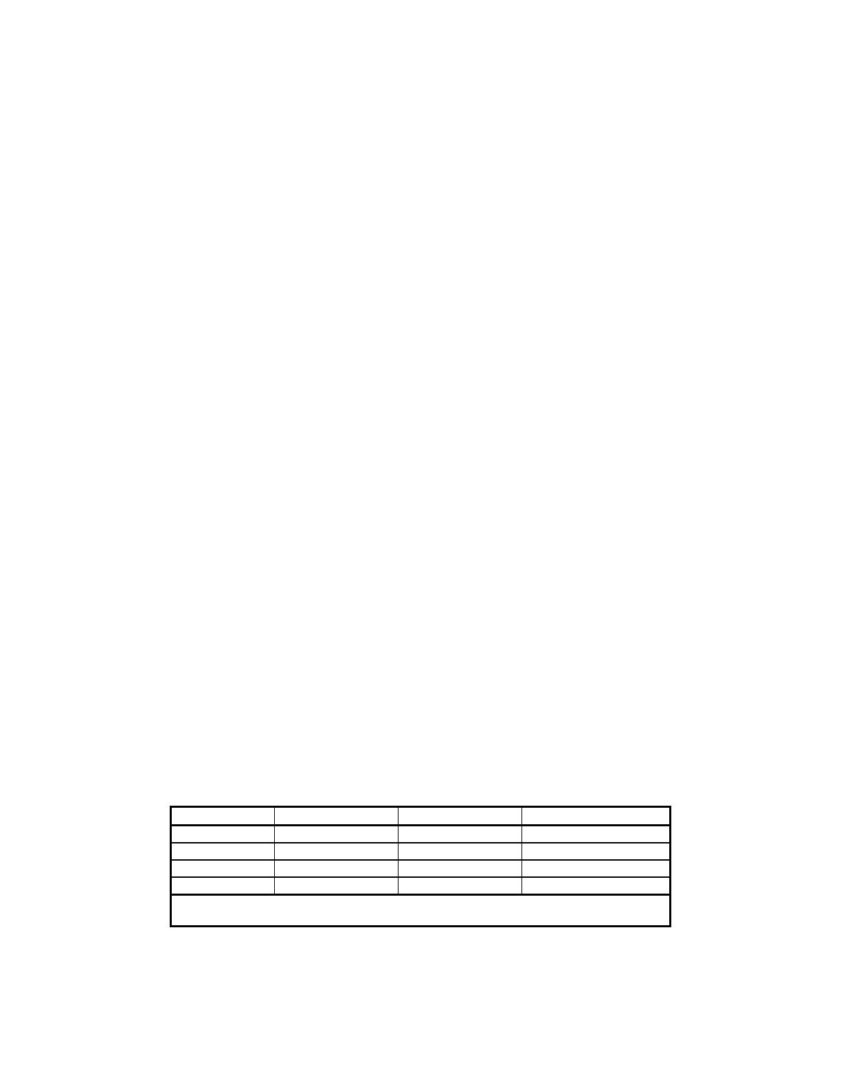
Supervisory Tone Detectors, Default Characteristics
The default bandwidths and thresholds of the tone detectors are as follows:
Tone Detector Bandwidth Turn-On Threshold Turn-Off Threshold
A 245 – 650 Hz –25 dBm –31 dBm
B 360 – 440 Hz –25 dBm –31 dBm
C Prefilter 0 – 500 Hz N/A N/A
C 50 – 110 Hz * *
* Tone Detector C will detect a difference tone within its bandwidth when the two tones present are in
the range –1 dBm to –26 dBm.
RCVDL56DPFL/SP, RCV56DPFL/SP, and RCV336DPFL/SP Designer’s Guide
1-8 1119
511 Pattern Generation/Detection
In a synchronous mode, a 511 pattern can be generated and detected (control bit S511). Use of this bit pattern during self-
test eliminates the need for external test equipment.
In-Band Secondary Channel
A full-duplex in-band secondary channel is provided in V.34 (all speeds) and V.32 bis/V.32 (7200 bps and above) modes.
Control bit SECEN enables and disables the secondary channel operation. The secondary channel operates in parallel data
mode with independent transmit and receive interrupts and data buffers. The main channel may operate in parallel or serial
mode.
In V.34 modes, the secondary channel rate is 200 bps.
In V.32 bis/V.32 modes, the secondary channel rate is 150 bps. This rate is also host programmable in V.32 bis/V.32 modes.
Transmit and Receive FIFO Data Buffers
Two (16+128)-byte first-in first-out (FIFO) data buffers allow the DTE/host to rapidly output up to 144 bytes of transmit data
and input up to 144 bytes of accumulated received data. The receiver FIFO is always enabled. The transmitter FIFO is
enabled by the FIFOEN control bit. TXHF and RXHF bits operate off the lower 16 bits and indicate the corresponding FIFO
buffer half full (8 or more bytes loaded) status. TXFNF and RXFNE bits indicate the TXFIFO buffer not full and RXFIFO
buffer not empty status, respectively. An interrupt mask register allows an interrupt request to be generated whenever the
TXFNF, RXFNE, RXHF, or TXHF status bit changes state. The 128-byte FIFO extensions are enabled by default and can be
disabled by clearing a bit in RAM. (See Section 4, Function 74.)
DMA Support Interrupt Request Lines
DMA support is available in synchronous, asynchronous, and HDLC parallel data modes. Control bit DMAE enables and
disables DMA support. When DMA support is enabled, the MDP ~RI and ~DSR lines are assigned to Transmitter Request
(TXRQ) and Receiver Request (RXRQ) hardware output interrupt request lines, respectively. The TXRQ and RXRQ signals
follow the assertion of the TDBE and RDBF interrupt bits thus allowing the DTE/host to respond immediately to the interrupt
request without masking out status bits to determine the interrupt source.
NRZI Encoding/Decoding
NRZI data encoding/decoding may be selected in synchronous and HDLC modes instead of the default NRZ (control bit
NRZIEN). In NRZ encoding, a 1 is represented by a high level and a 0 is represented by a low level. In NRZI encoding, a 1 is
represented by no change in level and a 0 is represented by a change in level.
ITU-T CRC-32 Support
ITU-T CRC-32 generation/checking may be selected instead of the default ITU-T CRC-16 in HDLC mode using DSP RAM
access.
Caller ID Demodulation
Caller ID information can be demodulated in V.23 1200 receive configuration and presented to the host/DTE in serial (RXD)
and parallel (RBUFFER) form.
Relay Control.
Direct control of the off-hook and talk/data relays is provided. Internal relay drivers allow direct connection to
the off-hook (RLYA) and talk/data (RLYB) relays. The talk/data relay output can optionally be used for pulse dial.
Speaker Interface
An analog speaker output (SPKR) is provided with on/off and volume control logic incorporated in the MDP. An external
amplifier is recommended if driving non-amplified speakers.
A digital speaker output (SPKMD) is provided which reflects the received analog input signal digitized to TTL high or low level
by an internal comparator to create a PC Card (PCMCIA)-compatible signal.
RCVDL56DPFL/SP, RCV56DPFL/SP, and RCV336DPFL/SP Designer’s Guide
1119 2-1
2. HARDWARE INTERFACE
2.1 HARDWARE INTERFACE SIGNALS
The functional interconnect diagram in Figure 2-1 (RCV336DPFL/SP), Figure 2-2 (RCV56DPFL/SP), and Figure 2-3
(RCVDL56DPFL/SP) show the typical MDP connections in a system. In these diagrams, any point that is active low is
represented by a small circle at the signal point.
Edge triggered inputs are denoted by a small triangle (e.g., TDCLK). An active low signal is indicated by a tilde preceding the
signal name (e.g., ~RESET).
A clock intended to activate logic on its rising edge (low-to-high transition) is called active low (e.g., ~RDCLK), while a clock
intended to activate logic on its falling edge (high-to-low transition) is called active high (e.g., TDCLK). When a clock input is
associated with a small circle, the input activates on a falling edge. If no circle is shown, the input activates on a rising edge.
The pin assignments for the MDP packaged in a single 144-pin TQFP are shown in Figure 2-4 and are listed in Table 2-1.
The hardware interface signals are described in Table 2-2.
The digital interface characteristics are defined in Table 2-3.
The analog interface characteristics are defined in Table 2-4.
The power requirements are defined in Table 2-5.
The absolute maximum ratings are listed in Table 2-6.
The timing for DTE host microprocessor interface bus waveforms is shown in Table 2-7. The host bus waveforms are
illustrated in Figure 2-5.
The DTE serial interface waveforms are illustrated in Figure 2-6.
RCVDL56DPFL/SP, RCV56DPFL/SP, and RCV336DPFL/SP Designer’s Guide
2-2 1119
XMD148F1 FID
RC336DPFL
RCV336DPFL
RCV336DPFL/SP
MODEM
DATA PUMP
(R6755:144-PIN TQFP)
RS0-RS4
CRYSTAL
XTLI
XTLO
TELEPHONE LINE/
TELEPHONE/
AUDIO INTERFACE
INTERFACE
TELEPHONE
LINE
~RLYA
~RLYB
RINGD
RIN
TXA1
TXA2
TELIN
TELOUT
MICV
MICM
SPK
SPKMD
RXA
TXA
+5V
AGND
DGND
POWER
SUPPLY
HOST
PROCESSOR
DECODER
~CS
~READ
~WRITE
DATA BUS (8) D0-D7
ADDRESS BUS (5) A0-A4
~RESET
IRQ
MIC/
SPEAKER
SPKR
MIC
TELEPHONE
LINE
TELOUT
TELIN
V.24
SERIAL
DTE
INTERFACE
~RDCLK
TDCLK
XTCLK
TXD
RXD
~RTS
~CTS
~DTR
~DSR
~RLSD
~RI
Figure 2-1. RCV336DPFL/SP Modem Functional Interface Signals
XMD180F1 FID
RC56DPFL
RCV56DPFL
RCV56DPFL/SP
MODEM
DATA PUMP
(R6765:144-PIN TQFP)
RS0-RS4
CRYSTAL
XTLI
XTLO
TELEPHONE LINE/
TELEPHONE/
AUDIO INTERFACE
INTERFACE
TELEPHONE
LINE
~RLYA
~RLYB
RINGD
RIN
TXA1
TXA2
TELIN
TELOUT
MICV
MICM
SPK
SPKMD
RXA
TXA
+5V
AGND
DGND
POWER
SUPPLY
HOST
PROCESSOR
DECODER
~CS
~READ
~WRITE
DATA BUS (8) D0-D7
ADDRESS BUS (5) A0-A4
~RESET
IRQ
MIC/
SPEAKER
SPKR
MIC
TELEPHONE
LINE
TELOUT
TELIN
V.24
SERIAL
DTE
INTERFACE
~RDCLK
TDCLK
XTCLK
TXD
RXD
~RTS
~CTS
~DTR
~DSR
~RLSD
~RI
Figure 2-2. RCV56DPFL/SP Modem Functional Interface Signals
  • Page 1 1
  • Page 2 2
  • Page 3 3
  • Page 4 4
  • Page 5 5
  • Page 6 6
  • Page 7 7
  • Page 8 8
  • Page 9 9
  • Page 10 10
  • Page 11 11
  • Page 12 12
  • Page 13 13
  • Page 14 14
  • Page 15 15
  • Page 16 16
  • Page 17 17
  • Page 18 18
  • Page 19 19
  • Page 20 20
  • Page 21 21
  • Page 22 22
  • Page 23 23
  • Page 24 24
  • Page 25 25
  • Page 26 26
  • Page 27 27
  • Page 28 28
  • Page 29 29
  • Page 30 30
  • Page 31 31
  • Page 32 32
  • Page 33 33
  • Page 34 34
  • Page 35 35
  • Page 36 36
  • Page 37 37
  • Page 38 38
  • Page 39 39
  • Page 40 40
  • Page 41 41
  • Page 42 42
  • Page 43 43
  • Page 44 44
  • Page 45 45
  • Page 46 46
  • Page 47 47
  • Page 48 48
  • Page 49 49
  • Page 50 50
  • Page 51 51
  • Page 52 52
  • Page 53 53
  • Page 54 54
  • Page 55 55
  • Page 56 56
  • Page 57 57
  • Page 58 58
  • Page 59 59
  • Page 60 60
  • Page 61 61
  • Page 62 62
  • Page 63 63
  • Page 64 64
  • Page 65 65
  • Page 66 66
  • Page 67 67
  • Page 68 68
  • Page 69 69
  • Page 70 70
  • Page 71 71
  • Page 72 72
  • Page 73 73
  • Page 74 74
  • Page 75 75
  • Page 76 76
  • Page 77 77
  • Page 78 78
  • Page 79 79
  • Page 80 80
  • Page 81 81
  • Page 82 82
  • Page 83 83
  • Page 84 84
  • Page 85 85
  • Page 86 86
  • Page 87 87
  • Page 88 88
  • Page 89 89
  • Page 90 90
  • Page 91 91
  • Page 92 92
  • Page 93 93
  • Page 94 94
  • Page 95 95
  • Page 96 96
  • Page 97 97
  • Page 98 98
  • Page 99 99
  • Page 100 100
  • Page 101 101
  • Page 102 102
  • Page 103 103
  • Page 104 104
  • Page 105 105
  • Page 106 106
  • Page 107 107
  • Page 108 108
  • Page 109 109
  • Page 110 110
  • Page 111 111
  • Page 112 112
  • Page 113 113
  • Page 114 114
  • Page 115 115
  • Page 116 116
  • Page 117 117
  • Page 118 118
  • Page 119 119
  • Page 120 120
  • Page 121 121
  • Page 122 122
  • Page 123 123
  • Page 124 124
  • Page 125 125
  • Page 126 126
  • Page 127 127
  • Page 128 128
  • Page 129 129
  • Page 130 130
  • Page 131 131
  • Page 132 132
  • Page 133 133
  • Page 134 134
  • Page 135 135
  • Page 136 136
  • Page 137 137
  • Page 138 138
  • Page 139 139
  • Page 140 140
  • Page 141 141
  • Page 142 142
  • Page 143 143
  • Page 144 144
  • Page 145 145
  • Page 146 146
  • Page 147 147
  • Page 148 148
  • Page 149 149
  • Page 150 150
  • Page 151 151
  • Page 152 152
  • Page 153 153
  • Page 154 154
  • Page 155 155
  • Page 156 156
  • Page 157 157
  • Page 158 158
  • Page 159 159
  • Page 160 160
  • Page 161 161
  • Page 162 162
  • Page 163 163
  • Page 164 164
  • Page 165 165
  • Page 166 166
  • Page 167 167
  • Page 168 168
  • Page 169 169
  • Page 170 170
  • Page 171 171
  • Page 172 172
  • Page 173 173
  • Page 174 174
  • Page 175 175
  • Page 176 176
  • Page 177 177
  • Page 178 178
  • Page 179 179
  • Page 180 180
  • Page 181 181
  • Page 182 182
  • Page 183 183
  • Page 184 184
  • Page 185 185
  • Page 186 186
  • Page 187 187
  • Page 188 188
  • Page 189 189
  • Page 190 190
  • Page 191 191
  • Page 192 192
  • Page 193 193
  • Page 194 194

Rockwell RC336DPFL Designer's Manual

Type
Designer's Manual

Ask a question and I''ll find the answer in the document

Finding information in a document is now easier with AI