Texas Instruments General-Purpose 3 V to 5.5 V 16-Bit 22-KSPS DSP Codec (Rev. F) Datasheet
- Type
- Datasheet

December 2001 HPA Data Acquisition
Data Manual
SLWS093F

IMPORTANT NOTICE
Texas Instruments Incorporated and its subsidiaries (TI) reserve the right to make corrections, modifications,
enhancements, improvements, and other changes to its products and services at any time and to discontinue
any product or service without notice. Customers should obtain the latest relevant information before placing
orders and should verify that such information is current and complete. All products are sold subject to TI’s terms
and conditions of sale supplied at the time of order acknowledgment.
TI warrants performance of its hardware products to the specifications applicable at the time of sale in
accordance with TI’s standard warranty. Testing and other quality control techniques are used to the extent TI
deems necessary to support this warranty. Except where mandated by government requirements, testing of all
parameters of each product is not necessarily performed.
TI assumes no liability for applications assistance or customer product design. Customers are responsible for
their products and applications using TI components. To minimize the risks associated with customer products
and applications, customers should provide adequate design and operating safeguards.
TI does not warrant or represent that any license, either express or implied, is granted under any TI patent right,
copyright, mask work right, or other TI intellectual property right relating to any combination, machine, or process
in which TI products or services are used. Information published by TI regarding third–party products or services
does not constitute a license from TI to use such products or services or a warranty or endorsement thereof.
Use of such information may require a license from a third party under the patents or other intellectual property
of the third party, or a license from TI under the patents or other intellectual property of TI.
Reproduction of information in TI data books or data sheets is permissible only if reproduction is without
alteration and is accompanied by all associated warranties, conditions, limitations, and notices. Reproduction
of this information with alteration is an unfair and deceptive business practice. TI is not responsible or liable for
such altered documentation.
Resale of TI products or services with statements different from or beyond the parameters stated by TI for that
product or service voids all express and any implied warranties for the associated TI product or service and
is an unfair and deceptive business practice. TI is not responsible or liable for any such statements.
Mailing Address:
Texas Instruments
Post Office Box 655303
Dallas, Texas 75265
Copyright 2001, Texas Instruments Incorporated

iii
Contents
Section Title Page
1 Introduction 1–1. . . . . . . . . . . . . . . . . . . . . . . . . . . . . . . . . . . . . . . . . . . . . . . . . . . . . .
1.1 Features 1–1. . . . . . . . . . . . . . . . . . . . . . . . . . . . . . . . . . . . . . . . . . . . . . . . . . .
1.2 Functional Block Diagram 1–3. . . . . . . . . . . . . . . . . . . . . . . . . . . . . . . . . . . .
1.3 Terminal Assignments 1–4. . . . . . . . . . . . . . . . . . . . . . . . . . . . . . . . . . . . . . . .
1.4 Ordering Information 1–5. . . . . . . . . . . . . . . . . . . . . . . . . . . . . . . . . . . . . . . . .
1.5 Terminal Functions 1–6. . . . . . . . . . . . . . . . . . . . . . . . . . . . . . . . . . . . . . . . . .
1.6 Definitions and Terminology 1–7. . . . . . . . . . . . . . . . . . . . . . . . . . . . . . . . . . .
1.7 Register Functional Summary 1–8. . . . . . . . . . . . . . . . . . . . . . . . . . . . . . . . .
2 Functional Description 2–1. . . . . . . . . . . . . . . . . . . . . . . . . . . . . . . . . . . . . . . . . . . .
2.1 Device Functions 2–1. . . . . . . . . . . . . . . . . . . . . . . . . . . . . . . . . . . . . . . . . . . .
2.1.1 Operating Frequencies 2–1. . . . . . . . . . . . . . . . . . . . . . . . . . . . . .
2.1.2 ADC Signal Channel 2–1. . . . . . . . . . . . . . . . . . . . . . . . . . . . . . . .
2.1.3 DAC Signal Channel 2–2. . . . . . . . . . . . . . . . . . . . . . . . . . . . . . . .
2.1.4 MIC Input 2–4. . . . . . . . . . . . . . . . . . . . . . . . . . . . . . . . . . . . . . . . . .
2.1.5 Antialiasing Filter 2–4. . . . . . . . . . . . . . . . . . . . . . . . . . . . . . . . . . .
2.1.6 Sigma-Delta ADC 2–4. . . . . . . . . . . . . . . . . . . . . . . . . . . . . . . . . . .
2.1.7 Decimation Filter 2–4. . . . . . . . . . . . . . . . . . . . . . . . . . . . . . . . . . .
2.1.8 Sigma-Delta DAC 2–4. . . . . . . . . . . . . . . . . . . . . . . . . . . . . . . . . . .
2.1.9 Interpolation Filter 2–4. . . . . . . . . . . . . . . . . . . . . . . . . . . . . . . . . .
2.1.10 Analog and Digital Loopback 2–5. . . . . . . . . . . . . . . . . . . . . . . . .
2.1.11 FIR Overflow Flag 2–5. . . . . . . . . . . . . . . . . . . . . . . . . . . . . . . . . .
2.1.12 FIR Bypass Mode 2–5. . . . . . . . . . . . . . . . . . . . . . . . . . . . . . . . . . .
2.1.13 Low-Power Mode 2–5. . . . . . . . . . . . . . . . . . . . . . . . . . . . . . . . . . .
2.1.14 Event-Monitor Mode 2–5. . . . . . . . . . . . . . . . . . . . . . . . . . . . . . . .
2.2 Reset and Power-Down Functions 2–6. . . . . . . . . . . . . . . . . . . . . . . . . . . . .
2.2.1 Software and Hardware Reset 2–6. . . . . . . . . . . . . . . . . . . . . . . .
2.2.2 Software and Hardware Power Down 2–6. . . . . . . . . . . . . . . . . .
2.3 Clock Source 2–7. . . . . . . . . . . . . . . . . . . . . . . . . . . . . . . . . . . . . . . . . . . . . . .
2.4 Data Out (DOUT) 2–7. . . . . . . . . . . . . . . . . . . . . . . . . . . . . . . . . . . . . . . . . . . .
2.4.1 Data Out, Master Mode 2–7. . . . . . . . . . . . . . . . . . . . . . . . . . . . . .
2.4.2 Data Out, Slave Mode 2–7. . . . . . . . . . . . . . . . . . . . . . . . . . . . . . .
2.5 Data In (DIN) 2–7. . . . . . . . . . . . . . . . . . . . . . . . . . . . . . . . . . . . . . . . . . . . . . .
2.6 FC (Hardware Secondary Communication Request) 2–7. . . . . . . . . . . . .
2.7 Frame-Sync Function for TLV320AIC10 2–7. . . . . . . . . . . . . . . . . . . . . . . .
2.7.1 Frame-Sync (FS) Function—Continuous-Transfer
Mode (Master Only) 2–9. . . . . . . . . . . . . . . . . . . . . . . . . . . . . . . . .
2.7.2 Frame-Sync (FS) Function—Fast-Transfer Mode
(Slave Only) 2–9. . . . . . . . . . . . . . . . . . . . . . . . . . . . . . . . . . . . . . .

iv
2.7.3 Frame-Sync (FS) Function—Master Mode 2–9. . . . . . . . . . . . .
2.7.4 Frame-Sync (FS) Function—Slave Mode 2–10. . . . . . . . . . . . . .
2.7.5 Frame-Sync Delayed (FSD) Function, Cascade Mode 2–10. . .
2.8 Multiplexed Analog Input and Output 2–11. . . . . . . . . . . . . . . . . . . . . . . . . . .
2.8.1 Multiplexed Analog Input 2–11. . . . . . . . . . . . . . . . . . . . . . . . . . . . .
2.8.2 Analog Output 2–12. . . . . . . . . . . . . . . . . . . . . . . . . . . . . . . . . . . . . .
2.8.3 Single-Ended Analog Input 2–12. . . . . . . . . . . . . . . . . . . . . . . . . . .
2.8.4 Single-Ended Analog Output 2–12. . . . . . . . . . . . . . . . . . . . . . . . .
3 Serial Communications 3–1. . . . . . . . . . . . . . . . . . . . . . . . . . . . . . . . . . . . . . . . . . .
3.1 Primary Serial Communication 3–1. . . . . . . . . . . . . . . . . . . . . . . . . . . . . . . .
3.2 Secondary Serial Communication 3–2. . . . . . . . . . . . . . . . . . . . . . . . . . . . .
3.2.1 Register Programming 3–3. . . . . . . . . . . . . . . . . . . . . . . . . . . . . .
3.2.2 Hardware Secondary Serial Communication Request 3–4. . . .
3.2.3 Software Secondary Serial Communication Request 3–5. . . .
3.3 Direct Configuration Mode 3–5. . . . . . . . . . . . . . . . . . . . . . . . . . . . . . . . . . . .
3.4 Continuous Data Transfer Mode 3–7. . . . . . . . . . . . . . . . . . . . . . . . . . . . . . .
3.5 DIN and DOUT Data Format 3–8. . . . . . . . . . . . . . . . . . . . . . . . . . . . . . . . . .
3.5.1 Primary Serial Communication DIN and
DOUT Data Format 3–8. . . . . . . . . . . . . . . . . . . . . . . . . . . . . . . . .
3.5.2 Secondary Serial Communication DIN and
DOUT Data Format 3–8. . . . . . . . . . . . . . . . . . . . . . . . . . . . . . . . .
3.5.3 Direct Configuration DCSI Data Format 3–8. . . . . . . . . . . . . . . .
4 Specifications 4–1. . . . . . . . . . . . . . . . . . . . . . . . . . . . . . . . . . . . . . . . . . . . . . . . . . . .
4.1 Absolute Maximum Ratings Over Operating Free-Air
Temperature Range 4–1. . . . . . . . . . . . . . . . . . . . . . . . . . . . . . . . . . . . . . . . . .
4.2 Recommended Operating Conditions 4–1. . . . . . . . . . . . . . . . . . . . . . . . . .
4.3 Electrical Characteristics Over Recommended Operating Free-Air
Temperature Range, AV
DD
= 5 V/3.3 V, DV
DD
= 5 V/3.3 V 4–1. . . . . . . .
4.3.1 Digital Inputs and Outputs, Fs = 8 kHz,
Output Not Loaded 4–1. . . . . . . . . . . . . . . . . . . . . . . . . . . . . . . . . .
4.3.2 ADC Path Filter, Fs = 8 kHz 4–2. . . . . . . . . . . . . . . . . . . . . . . . . .
4.3.3 ADC Dynamic Performance, Fs = 8 kHz 4–2. . . . . . . . . . . . . . .
4.3.4 ADC Channel Characteristics 4–3. . . . . . . . . . . . . . . . . . . . . . . .
4.3.5 DAC Path Filter, Fs= 8 kHz 4–3. . . . . . . . . . . . . . . . . . . . . . . . . . .
4.3.6 DAC Dynamic Performance 4–3. . . . . . . . . . . . . . . . . . . . . . . . . .
4.3.7 DAC Channel Characteristics 4–4. . . . . . . . . . . . . . . . . . . . . . . .
4.3.8 Op-Amp Interface (A1, A3, A4) 4–4. . . . . . . . . . . . . . . . . . . . . . .
4.3.9 Power-Supply Rejection 4–4. . . . . . . . . . . . . . . . . . . . . . . . . . . . .
4.3.10 Power Supply 4–5. . . . . . . . . . . . . . . . . . . . . . . . . . . . . . . . . . . . . .
4.4 Timing Requirements 4–5. . . . . . . . . . . . . . . . . . . . . . . . . . . . . . . . . . . . . . . .
4.4.1 Master Mode Timing Requirements 4–5. . . . . . . . . . . . . . . . . . .

v
5 Parameter Measurement Information 5–1. . . . . . . . . . . . . . . . . . . . . . . . . . . . . . .
6 Mechanical Information 6–1. . . . . . . . . . . . . . . . . . . . . . . . . . . . . . . . . . . . . . . . . . .
Appendix A—Register Set A–1. . . . . . . . . . . . . . . . . . . . . . . . . . . . . . . . . . . . . . . . . . . .
List of Illustrations
Figure Title Page
2–1 Timing Sequence of ADC Channel (Primary Communication Only) 2–1. . . . . .
2–2 Timing Sequence of ADC Channel (Primary and Secondary
Communication) 2–2. . . . . . . . . . . . . . . . . . . . . . . . . . . . . . . . . . . . . . . . . . . . . . . .
2–3 Timing Sequence of DAC Channel (Primary Communication Only) 2–3. . . . . .
2–4 Timing Sequence of DAC Channel (Primary and
Secondary Communication) 2–3. . . . . . . . . . . . . . . . . . . . . . . . . . . . . . . . . . . . . .
2–5 Typical Microphone Interface 2–4. . . . . . . . . . . . . . . . . . . . . . . . . . . . . . . . . . . . . . .
2–6 Event Monitor Mode Timing 2–5. . . . . . . . . . . . . . . . . . . . . . . . . . . . . . . . . . . . . . . .
2–7 Internal Power-Down Logic 2–6. . . . . . . . . . . . . . . . . . . . . . . . . . . . . . . . . . . . . . . . .
2–8 Timing Diagram for the FS Pulse Mode (M1M0 = 00) 2–8. . . . . . . . . . . . . . . . . .
2–9 Timing Diagram for the SPI_CP0 Mode (M1M0 = 01) 2–8. . . . . . . . . . . . . . . . . .
2–10 Timing Diagram for the SPI_CP1 Mode (M1M0 = 10) 2–8. . . . . . . . . . . . . . . . .
2–11 Timing Diagram for the FS Frame Mode (M1M0 = 11) 2–9. . . . . . . . . . . . . . . . .
2–12 Master Device Frame-Sync Signal With Primary and Secondary
Communication ( No Slaves) 2–9. . . . . . . . . . . . . . . . . . . . . . . . . . . . . . . . . . . . .
2–13 Master Device’s FS Output to DSP and FSD Output to the Slave 2–10. . . . . . .
2–14 Cascade Mode Connection (to DSP Interface) 2–10. . . . . . . . . . . . . . . . . . . . . . .
2–15 Master-Slave Frame-Sync Timing 2–11. . . . . . . . . . . . . . . . . . . . . . . . . . . . . . . . . .
2–16 INP and INM Internal Self-Biased
(AV
DD
/2) Circuit 2–11. . . . . . . . . . . . . . . . . . .
2–17 Differential Output Drive (Ground-Referenced) 2–12. . . . . . . . . . . . . . . . . . . . . . .
2–18 Single-Ended Input 2–12. . . . . . . . . . . . . . . . . . . . . . . . . . . . . . . . . . . . . . . . . . . . . . .
2–19 Single-Ended Output 2–12. . . . . . . . . . . . . . . . . . . . . . . . . . . . . . . . . . . . . . . . . . . . .
3–1 Primary Serial Communication Timing 3–1. . . . . . . . . . . . . . . . . . . . . . . . . . . . . . .
3–2 Hardware and Software Secondary Communication Request 3–2. . . . . . . . . . .
3–3 Device 3/Register 1 Read Operation Timing Diagram 3–3. . . . . . . . . . . . . . . . . .
3–4 Device 3/Register 1 Write Operation Timing Diagram 3–4. . . . . . . . . . . . . . . . . .
3–5 FS Output When Hardware Secondary Serial Communication
Is Requested Only Once (No Slave) 3–4. . . . . . . . . . . . . . . . . . . . . . . . . . . . . . .
3–6 Output When Hardware Secondary Serial Communication Is Requested
(Three Slaves) 3–5. . . . . . . . . . . . . . . . . . . . . . . . . . . . . . . . . . . . . . . . . . . . . . . . .
3–7 FS Output During Software Secondary Serial Communication Request
(No Slave) 3–5. . . . . . . . . . . . . . . . . . . . . . . . . . . . . . . . . . . . . . . . . . . . . . . . . . . . .
3–8 Direct Configuration 3–6. . . . . . . . . . . . . . . . . . . . . . . . . . . . . . . . . . . . . . . . . . . . . . .

vi
3–9 Direct Configuration Mode Timing 3–7. . . . . . . . . . . . . . . . . . . . . . . . . . . . . . . . . . .
3–10 Continuous Data Transfer Mode Timing 3–7. . . . . . . . . . . . . . . . . . . . . . . . . . . . .
3–11 Primary Communication DIN and DOUT Data Format 3–8. . . . . . . . . . . . . . . .
3–12 Secondary Communication DIN and DOUT Data Format 3–8. . . . . . . . . . . . . .
3–13 Direct Communication DCSI Data Format 3–8. . . . . . . . . . . . . . . . . . . . . . . . . . .
5–1 FC, FS and FSD Timing 5–1. . . . . . . . . . . . . . . . . . . . . . . . . . . . . . . . . . . . . . . . . . .
5–2 Serial Communication Timing 5–1. . . . . . . . . . . . . . . . . . . . . . . . . . . . . . . . . . . . . . .
5–3 FFT–ADC Channel 5–2. . . . . . . . . . . . . . . . . . . . . . . . . . . . . . . . . . . . . . . . . . . . . . . .
5–4 FFT–ADC Channel 5–2. . . . . . . . . . . . . . . . . . . . . . . . . . . . . . . . . . . . . . . . . . . . . . . .
5–5 FFT–DAC Channel 5–3. . . . . . . . . . . . . . . . . . . . . . . . . . . . . . . . . . . . . . . . . . . . . . . .
5–6 FFT–DAC Channel 5–3. . . . . . . . . . . . . . . . . . . . . . . . . . . . . . . . . . . . . . . . . . . . . . . .
5–7 FFT–ADC Channel 5–4. . . . . . . . . . . . . . . . . . . . . . . . . . . . . . . . . . . . . . . . . . . . . . . .
5–8 FFT–ADC Channel 5–4. . . . . . . . . . . . . . . . . . . . . . . . . . . . . . . . . . . . . . . . . . . . . . . .
5–9 FFT–DAC Channel 5–5. . . . . . . . . . . . . . . . . . . . . . . . . . . . . . . . . . . . . . . . . . . . . . . .
5–10 FFT–DAC Channel 5–5. . . . . . . . . . . . . . . . . . . . . . . . . . . . . . . . . . . . . . . . . . . . . . .
List of Tables
Table Title Page
2–1 Serial Interface Modes 2–8. . . . . . . . . . . . . . . . . . . . . . . . . . . . . . . . . . . . . . . . . . . . .
3–1 Least Significant Bit Control Function 3–2. . . . . . . . . . . . . . . . . . . . . . . . . . . . . . . .

1–1
1 Introduction
The TLV320AIC10 provides high resolution signal conversion from digital-to-analog (D/A) and from analog-to-digital
(A/D) using oversampling sigma-delta technology. It allows 2-to-1 MUX inputs with built-in antialiasing filter and
amplification for general-purpose applications such as telephone hybrid interface, electret microphone preamp, etc.
Both IN and AUX inputs accept normal analog signals. This device consists of a pair of 16-bit synchronous serial
conversion paths (one for each direction), and includes an interpolation filter before the DAC and a decimation filter
after the ADC. The FIR filters can be bypassed to offer flexibility and power savings. Other overhead functions provide
on-chip include timing (programmable sample rate, continuous data transfer, and FIR bypass) and control
(programmable-gain amplifier, communication protocol, etc.). The sigma-delta architecture produces high-resolution
analog-to-digital and digital-to-analog conversion at low system cost.
The TLV320AIC10 design enhances communication with the DSP. The continuous data transfer mode fully supports
TI’s DSP autobuffering (ABU) to reduce DSP interrupt service overhead. The automatic cascading detection (ACD)
makes cascade programming simple and supports a cascade operation of one master and up to seven slaves. The
direct-configuration mode for host interface uses a single-wire serial port to directly program internal registers without
interference from the data conversion serial port, or without resetting the entire device. The event monitor mode
allows the DSP to monitor external events like phone off-hook ring detection.
In the lower-power mode, the TLV320AIC10 converts data at a sampling rate of 8 KSPS consuming only 39 mW.
The programmable functions of this device are configured through a serial interface that can be gluelessly interfaced
to any DSP that accepts 4-wire serial communications, such as the TMS320Cxx. The options include software reset,
device power-down, separate control for ADC and DAC turnoff, communications protocol, signal-sampling rate, gain
control, and system-test modes, as outlined in Appendix A.
The TLV320AIC10 is particularly suitable for a variety of applications in hands-free car kits, VOIP, cable modem,
speech, and the telephony area including low-bit rate, high-quality compression, speech enhancement, recognition,
and synthesis. Its low-group delay characteristic makes it suitable for single or multichannel active-control
applications.
The TLV320AIC10 is characterized for commercial operation from 0°C to 70°C, and industrial operation from –40°C
to 85°C.
1.1 Features
• C54xx software driver available
• 16-bit oversampling sigma-delta A/D converter
• 16-bit oversampling sigma-delta D/A converter
• Maximum output conversion rate:
– 22 ksps with on-chip FIR filter
– 88 ksps with FIR bypassed
• Voiceband bandwidth in FIR-bypassed mode and final sampling rate at 8 ksps
– 90-dB SNR/ADC and 87-dB SNR/DAC with DSPs FIR (FIR bypassed at 88 ksps/5 V)
– 87-dB SNR/ADC and 85-dB SNR/DAC with DSPs FIR (FIR bypassed at 88 ksps/3.3 V)
• On-chip FIR produced 84-dB SNR for ADC and 85-dB SNR for DAC over 11-kHz BW
• Built-in functions including PGA, antialiasing analog filter, and operational amplifiers for general-purpose
interface (such as MIC interface and hybrid interface)

1–2
• Glueless serial port interface to DSPs (TI TMS320Cxx, SPI, or standard DSPs)
• Automatic cascading detection (ACD) makes cascade programming simple and allows up to 8 devices to
be connected in cascade.
• On-fly reconfiguration modes include secondary-communication mode and direct-configuration mode (host
interface).
• Continuous data-transfer mode for use with autobuffering (ABU) to reduce DSP interrupt service overhead
• Event-monitor mode provides external-event control, such as RING/OFF-HOOK detection
• Programmable ADC and DAC conversion rate
• Programmable input and output gain control
• Separate software control for ADC and DAC power-down
• Analog (3-V to 5.5-V) supply operation
• Digital (3-V to 5.5-V) supply operation
• Power dissipation (P
D
) of 39 mWrms typical for 8-ksps at 3.3 V
• Hardware power-down mode to 0.5 mW
• Internal and external reference voltage (V
ref
)
• Differential and single-ended analog input/output
• 2s-complement data format
• Test mode, which includes digital loopback and analog loopback
• 600-ohm output driver

1–3
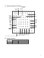
1.2 Functional Block Diagram
Sigma–
Delta
ADC
Sinc
Filter
Low
Pass
Filter
Sigma–
Delta
DAC
ADREFP
ADREFM
MCLK
Interface
Circuit
Div
256xN
DIN
M/S
FSD
FS
SCLK
M0
M1
OUTP
OUTM
PGA
PGA
DOUT
Internal Clock Circuit
FIR
Filter
Analog
Loopback
Decimation Filter
Anti–
Aliasing
Filter
VMID
@ 5 mA
V
ALTI
FLAG
FC
DCSI
DAREFP
DAREFM
MUX
AURXM
AURXFP
INM
INP
AURXCP
1.5 V
or
2.5V
DTXOP
DTXIM
Receiver or MIC Amp
Transmitter Amp
DTXIP
DTXOM
+
–
+
–
–
+
A3
A4
A2
A1
Sinc
Filter
FIR
Filter
Interpolation Filter
Digital
Loopback
SW4
SW5
SW6
SW2 SW3
SW1
Note: Switches SWx are Controlled by Bit D6 of Control Register 1.
ref

1–4
1.3 Terminal Assignments
14 15
NC
NC
AV
DD2
AV
SS
NC
NC
DV
DD2
DV
SS
NC
M/S
ALTIN
DCSI
36
35
34
33
32
31
30
29
28
27
26
25
16
1
2
3
4
5
6
7
8
9
10
11
12
AURXFP
AURXM
AURXCP
DTXOP
DTXOM
DTXIP
DTXIM
OUTP
OUTM
M0
M1
PWRDWN
17 18 19 20
FILT
47 46 45 44 4348 42
INM
INP
AV
AV
NC
FS
FLAG
FC
DV
DIN
NC
SCLK
MCLK
FSD
40 39 3841
21 22 23 24
37
13
NC
VMID
DV
RESET
DOUT
PFB PACKAGE
(TOP VIEW)
SS
DD1
DD1
SS
SS
AV
NC
SS
AV
NC
NOTE: All NC pins should be left unconnected.

1–5
1.3 Terminal Assignments (Continued)
98765
A
B
C
D
E
F
321
G
H
J
4
ALTIN
MCLK
PWRDWN
FSD
FLAG
AVSS
AVDD2
AVSS
AVDD1
FILT
AURXFP
AURXM
AVSS
VMID
RESET
DIN
DVDD2
INP
DVDD1
DTXIM
AURXCP
DTXOM
M0
OUTP
NC
NC
NC
NC
NC
NC
NC
NC NC
NC NC
NC NC
NC NC
NC NC NC
NC
NC
NC
NC NC
NC NC
NC NC
DTXOP
DTXIP
OUTM
M1
NC
DVSS
DOUT
SCLK
FS
FC
DCSI
M/S
NC
DVSS
NC
NC
NC NC
NC
AVSS
AVSS
INM
NC
NC NC
NC
NCNC
GQE PACKAGE
(TOP VIEW)
NOTE: All NC pins should be left unconnected.
NC
1.4 Ordering Information
T
PACKAGES
T
A
48-PIN TQFP PFB 80-PIN MicroStar Junior GQE
0°C to 70°C TLV320AIC10C TLV320AIC10CGQE
–40°C to 85°C TLV320AIC10I TLV320AIC10IGQE

1–6
1.5 Terminal Functions
TERMINALS
I/O
NAME
NO.
I/O
DESCRIPTION
NAME
PFB GQE I/O
DESCRIPTION
ALTIN 26 G9 I Serial input in the event monitor mode. Tie this pin to low if not used.
AURXCP 3 C1 I Receiver-path/GP amplifier noninverting input. It needs to be connected to AV
SS
if not used.
AURXM 2 C2 I Receiver-path amplifier A1 inverting input, or inverting input to auxiliary analog input. It needs to be
connected to AV
SS
if not used. Can also be used for general-purpose amplification.
AURXFP 1 B1 I Receiver-path amplifier A1 feedback, or noninverting input to auxiliary analog input. It needs to be
connected to AV
SS
if not used. Can also be used for general-purpose amplification.
AV
DD1
45 B4 I Analog power supply
AV
DD2
34 D8 I Analog power supply
AV
SS
33, 40,
42, 46
A3, B3,
B5, B6,
D9
I Analog ground
DCSI 25 G8 I Direct configuration serial input for directly programming of internal control registers. Tie this pin to
high if not used.
DIN 17 J4 I Data input. DIN receives the DAC input data and register data from the external digital signal
processor (DSP), and is synchronized to SCLK and FS. Data is latched at the falling edge of SCLK
when FS is low. DIN is at high impedance when FS is not activated.
DOUT 16 H4 O Data output. DOUT transmits the ADC output bits and registers data, and is synchronized to SCLK
and FS. Data is sent out at the rising edge of SCLK when FS is low. DOUT is at high impedance when
FS is not activated.
DTXIM 7 E1 I Transmitter-path amplifier A3 analog inverting input. Can also be used for general-purpose
amplification.
DTXIP 6 E2 I Transmitter-path amplifier A4 analog noninverting input. Can also be used for general-purpose
amplification.
DTXOM 5 D1 O Transmitter path amplifier A4 feedback for negative output. Can also be used for general-purpose
amplification.
DTXOP 4 D2 O Transmitter path amplifier A3 feedback for positive output. Can also be used for negative output.
DV
DD1
15 J3 I Digital power supply
DV
DD2
30 E9 I Digital power supply
DV
SS
14, 29 E8, H3 I Digital ground
FC 24 H7 I Hardware request for secondary communication. Tie this pin to low if not used.
FILT 38 B7 O Bandgap filter. FILT is provided for decoupling of the bandgap reference, and provides 2.5 V. The
optimal capacitor value is 0.1 µF (ceramic). This voltage node should be loaded only with a
high-impedance dc load.
FLAG 23 J7 O Controlled by bit D4 of control register 3. If D4=0 (default), the FLAG pin outputs the communication
flag that goes low/high to indicate primary-communication/secondary-communication interval,
respectively. If D4=1, the FLAG pin outputs the value of D3.
FS 22 H6 I/O Frame sync. When FS goes low, DIN begins receiving data bits and DOUT begins transmitting data
bits. In master mode, FS is internally generated and is low during data transmission to DIN and from
DOUT. In slave mode, FS is externally generated.
FSD 21 J6 O Frame-sync delayed output. The FSD output synchronizes a slave device to the frame sync of the
master device. FSD is applied to the slave FS input and has the same duration as the master FS
signal. Requires a pullup resistor if not used.
INM 48 B2 I Inverting input to analog modulator. INM requires an external R-C antialias filter with low output
impedance if the internal antialias filter is bypassed.
INP 47 A2 I Noninverting input to analog modulator. INP requires an external R-C antialias filter with low output
impedance if the internal antialias filter is bypassed.
M0 10 G1 I Combine with M1 to select serial interface mode (frame-sync mode)
M1 11 G2 I Combine with M0 to select serial interface mode (frame-sync mode)

1–7
1.5 Terminal Functions (Continued)
TERMINALS
I/O
NAME
NO.
I/O
DESCRIPTION
NAME
PFB GQE I/O
DESCRIPTION
MCLK 20 J5 I Master clock. MCLK derives the internal clocks of the sigma-delta analog interface circuit.
M/S 27 F8 I Master/slave select input. When M/S is high, the device is the master, and when is low, it is a slave.
NC 18, 28,
31, 32,
35, 36,
37, 39,
41, 44
A6, A7,
C9, C8,
F9
No connection
OUTM 9 F2 O DACs inverting output. OUTM is functionally identical with and complementary to OUTP.
OUTP 8 F1 O DACs noninverting output. OUTP can also be used alone for single-ended operation.
PWRDWN 12 H1 I Power down. When PWRDWN is pulled low, the device goes into a power-down mode, the serial
interface is disabled, and most of the high-speed clocks are disabled. However, all register values are
sustained and the device resumes full-power operation without reinitialization when PWRDWN is
pulled high again. PWRDWN
resets the counters only and preserves the programmed register
contents. See paragraph 2.2.2 for more information.
RESET 13 J2 I The reset function is provided to initialize all the internal registers to their default values. The serial
port can be configured to the default state accordingly. See Appendix A, Register Set, and Subsection
2.2, Reset and Power-Down Functions for detailed descriptions. All RESET pins of devices in
cascade must be tied together.
SCLK 19 H5 I/O Shift clock. SCLK signal clocks serial data into DIN and out of DOUT during the frame-sync interval.
When configured as an output (M/S
high), SCLK is generated internally by multiplying the frame-sync
signal frequency by 256 (cascade devices < 5) or 512 (cascade devices > 4). When configured as an
input (M/S low), SCLK is generated externally and must be synchronous with the master clock and
frame sync.
VMID 43 A4 O Reference voltage output at AVDD/2
1.6 Definitions and Terminology
Data transfer interval The time during which data is transferred from DOUT to DIN. The interval is 16 shift clocks
and the data transfer is initiated by the falling edge of the FS signal.
Signal data This refers to the input signal and all of the converted representations through the ADC
channel, and the signal through the DAC channel to the analog output. This is in contrast
with the purely-digital software control data.
Primary
communication
Primary communication refers to the digital data-transfer interval. Since the device is
synchronous, the signal data words from the ADC channel and to the DAC channel occur
simultaneously.
Secondary
communication
Secondary communication refers to the digital control and configuration data-transfer
interval into DIN, and the register read-data cycle from DOUT. The data transfer occurs
when requested by hardware or software.
SPI Serial peripheral interface standard set by Motorola
Frame/pulse sync Frame/pulse sync refers only to the falling edge of the signal FS that initiates the
data-transfer interval. The primary FS starts the primary communication, and the
secondary FS starts the secondary communication.
Frame/pulse sync and
sampling period
Frame/pulse sync and sampling period is the time between falling edges of successive
primary FS signals and it is always equal to 256xSCLK if the number of cascading devices
is less than 5, or 512 xSCLK if the number of cascading devices is greater than 4.
f
s
The sampling frequency
ADC channel ADC channel refers to all signal-processing circuits between the analog input and the
digital conversion result at DOUT.

1–8
DAC channel DAC channel refers to all signal-processing circuits between the digital data word applied
to DIN and the differential output analog signal available at OUTP and OUTM.
Host A host is any processing system that interfaces to DIN, DOUT, SCLK, FS, and/or MCLK.
PGA Programmable gain amplifier
FIR Finite-duration impulse response
DCSI Direct configuration serial interface with host
1.7 Register Functional Summary
There are five control registers which are used as follows:
Register 0 The no-op register. Addressing register 0 allows secondary-communication request without altering any
other registers.
Register 1 Control register 1. The data in this register has the following functions:
• Produce the output flag to indicate a decimator FIR filter overflow (read cycle only)
• Enable of general-purpose operational amplifiers A1, A3, and A4
• Enable/bypass ADCs analog antialiasing filter
• Select normal or auxiliary analog input
• Control 16-bit or (15+1)-bit mode of DAC operation
• Activate software reset
• Enable/bypass the decimator FIR filter
• Enable/bypass the interpolator FIR filter
Register 2 Control register 2. The data in this register has the following functions:
• Control of the low-power mode that converts data at the rate of 8 ksps
• Control of the N-divide register that determines the filter clock rate and sample period
Register 3 Control register 3. The data in this register has the following functions:
• Software power down
• Selection of analog loopback, digital loopback, and event monitor mode
• Control of continuous data transfer mode
• Control of the value of one-bit general-purpose output flag
• Control the output of FLAG pin
• Enable/disable ADC path
• Enable/disable DAC path
• Control of 16-bit or (15+1)-bit mode of ADC operation
Register 4 Control register 4. The data in this register has the following functions:
• Control of the 4-bit gain of input PGA
• Control of the 4-bit gain of output PGA

2–1
2 Functional Description
2.1 Device Functions
2.1.1 Operating Frequencies
The sampling frequency represented by the frequency of the primary communication is derived from the master clock
(MCLK) input with the following equation:
Fs = Sampling (conversion) frequency = MCLK/(256 × N), N = 1, 2..., 32
The inverse of the sampling frequency is the time between the falling edges of two successive primary frame-sync
signals. This time is the conversion period. For example, to set the conversion rate to 8 kHz, MCLK = 256 × N × 8000.
NOTE:The value of N is defined in control register 2 and its power-up value is 32.
2.1.2 ADC Signal Channel
Both IN (INP, INM) and AUX (AURXFP, AURXM) inputs can use the built-in antialiasing filter that can be bypassed
by writing a 1 to bit D5 of control register 1. The AUX input can also be connected to the general-purpose amplifier
A1 for general-purpose applications, such as electret-microphone interface and 2-to-4-wire hybrid interface, by
writing a 1 to bit D6 of control register 1. Bit D4 of control register 1 selects between IN or AUX for the ADC. The
selected input signal is amplified by the PGA and applied to the ADC input. The ADC converts the signal into
discrete-output digital words in 2s-complement data format, corresponding to the analog-signal value at sampling
time. These 16-bit (or 15-bit) digital words, representing sampled values of the analog input signal after PGA, are
clocked out of the serial port (DOUT) at the positive edge of SCLK during the frame-sync (FS) interval at the rate of
one bit for each SCLK and one word for each primary communication. During secondary communication, the data
previously programmed into the registers can be read out. If a register read is not required, all 16 bits are cleared to
0 in the secondary communication. This read operation is accomplished by sending the appropriate register address
(D11-D9) with the read bit (D12) set to 1 during present secondary communication. The timing sequence is shown
in Figures 2–1 and 2–2.
The decimation FIR filter can be bypassed by writing a 1 to bit D2 of control register 1. The whole ADC channel can
be turned off for power savings by writing 01 to bits D2 and D1 of control register 3.
D0
16 SCLKs
SCLK
FS
DOUT
(16-bit)
DOUT
(15+1-bit)
D1
MSB LSB
LSB
D15
M/SD1
0 1 15 16
MSB
D15
D14
D14
……
……
……
……
NOTES: A. M/S is used to indicate whether the 15-bit data comes from a master or a slave device (master: M/S=1, slave: M/S=0).
B. The MSB (D15) is stable (the host can latch the data in at this time) at the falling edging of SCLK number 0; the last bit (D0,M/S)
is stable at the falling edging of SCLK number 15.
Figure 2–1. Timing Sequence of ADC Channel (Primary Communication Only)

2–2
FS
DOUT
(16-bit)
DOUT
(15+1-bit)
Primary Secondary
16 SCLKs
# SCLKs Per Sampling Period (See Note C)
16–bit ADC Data
15–bit ADC Data + M/S
M/S+ Register Data/
M/S+ All 0 (See Note A)
# SCLKs (See Note B)
M/S+ Register Data/
M/S+ All 0 (See Note A)
Primary
16 SCLKs
NOTES: A. M/S bit (D15) in the secondary communication is used to indicate whether the register data (address and content) come from a
master device or a slave device if read bit is set. Otherwise, it is all 0s except M/S bit (master: M/S=1, slave: M/S=0).
B. The number of SCLKs between FS (primary) and FS (secondary) is 128 if cascading devices are less than 5, or 256 if cascading
devices are greater than 4.
C. The number of SCLKs per data sampling period is 256 if cascading devices are less than 5, or 512 if cascading devices are greater
than 4.
Figure 2–2. Timing Sequence of ADC Channel (Primary and Secondary Communication)
2.1.3 DAC Signal Channel
DIN received the 16-bit serial data word (2s complement) from the host during the primary communication interval.
These 16-bit digital words, representing analog output signal before PGA, are clocked into the serial port (DIN) at
the falling edge of SCLK during the frame-sync interval, one bit for each SCLK and one word for each primary
communication interval. The data are converted to a pulse train by the sigma-delta DAC comprised of a
digital-interpolation filter and a digital 1-bit modulator. The output of the modulator is then passed to an internal
low-pass filter to complete the signal reconstruction. Finally, the resulting analog signal applied to the input of a
programmable-gain amplifier is capable of differentially driving a 600-ohm load at OUTP and OUTM. The timing
sequence is shown in Figure 2–3.
During secondary communication, the digital control and configuration data, together with the register address, are
clocked in through DIN (see Appendix A for register map). These 16-bit data are used either to initialize the register
or read out register content through DOUT. If a register initialization is not required, a no-operation word (D15-D9 are
all set to 0) can be used. If D12 is set to 1, the content of the control register, specified by D7-D0, are sent out through
DOUT during the same secondary communication (see Section 2.1.5). The timing sequence is shown in Figure 2–4.
The interpolation FIR filter can be bypassed by writing a 1 to bit D2 of control register 1. The whole DAC channel can
be turned off for power savings by writing 10 to bits D2 and D1 of control register 3.

2–3
D0
16 SCLKs
SCLK
FS
DIN
(16-bit)
DIN
(15+1-bit)
D1
MSB LSB
LSB
D15
D0=0D1
0 1 15 16
MSB
D15
D14
D14
……
……
……
……
14
(See Note A)
NOTE A: d0 = 0 means no secondary-communication request (software secondary-request control, see Section 3.2).
Figure 2–3. Timing Sequence of DAC Channel (Primary Communication Only)
FS
DIN (16-bit)
(See Note A)
DIN
(15+1-bit)
Primary Secondary
16 SCLKs
# SCLKs Between Sampling Period (See Note D)
16–bit DAC Data
# SCLKs Between
Primary
16 SCLKs
FS (Primary) and
FS (Secondary)
(See Note C)
15–bit DAC Data +
D0 = 1 (See Note B)
Register Read/Write
Register Read/Write
NOTES: A. FC has to be set high for a secondary communication request when 16-bit DAC data format is used (see Section 3.2).
B. D0 = 1 means secondary communication request (software secondary request control, see Section 3.2)
C. The number of SCLKs between FS (Primary) and FS (Secondary) is 128 if cascading devices are less than 5, or 256 if cascading
devices are greater than 4.
D. The number of SCLKs per data sampling period is 256 if cascading devices are less than 5, or 512 if cascading devices are greater
than 4.
Figure 2–4. Timing Sequence of DAC Channel (Primary and Secondary Communication)

2–4
2.1.4 MIC Input
The auxiliary inputs (AURXFP, AURXCP, and AURXM) can be programmed to interface with a microphone such as
an electret microphone, as illustrated in Figure 2.5, by writing a 1 to bit D6 and D4 of control register 1. Enabling MIC
input with DG automatically selects AURx channel for ADC input.
Sigma-
Delta
ADC
PGA
TLV320AIC10
Anti-
Aliasing
Filter
AURXFP
Electret
Microphone
MIC_BIAS VMID
10 kΩ
AURXM
AURXCP
S2D
+
–
1 kΩ
10 kΩ
0.1 µF
V
ref
Figure 2–5. Typical Microphone Interface
2.1.5 Antialiasing Filter
The built-in antialiasing filter has a 3-dB cutoff frequency of 70 kHz.
2.1.6 Sigma-Delta ADC
The sigma-delta analog-to-digital converter is a sigma-delta modulator with 128× oversampling. The ADC provides
high-resolution, low-noise performance using oversampling techniques. Due to the oversampling employed, only
single-pole RC filters are required on the analog inputs.
2.1.7 Decimation Filter
The decimation filters reduce the digital data rate to the sampling rate. This is accomplished by decimating with a ratio
of 1:64. The output of the decimation filter is a 16-bit 2s-complement data word clocking at the sample rate selected
for that particular data channel. The BW of the filter is 0.45 × FS and scales linearly with the sample rate.
2.1.8 Sigma-Delta DAC
The sigma-delta digital-to-analog converter is a sigma-delta modulator with 128× oversampling. The DAC provides
high-resolution, low-noise performance using oversampling techniques.
2.1.9 Interpolation Filter
The interpolation filter resamples the digital data at a rate of 64 times the incoming sample rate. The high-speed data
output from the interpolation filter is then used in the sigma-delta DAC. The BW of the filter is 0.45 x FS and scales
linearly with the sample rate.

2–5
2.1.10 Analog and Digital Loopback
The analog and digital loopbacks provide a means of testing the modem data ADC/DAC channels and can be used
for in-circuit system level tests. The analog loopback routes the DAC low-pass filter output into the analog input where
it is then converted by the ADC to a digital word. The digital loopback routes the ADC output to the DAC input on the
device. Analog loopback is enabled by writing 01 to bits D7 and D6 respectively in control register 3. Digital loopback
is enabled by writing 10 to bits D7 and D6 in control register 3 (see Appendix A).
2.1.11 FIR Overflow Flag
The decimator FIR filter sets an overflow flag (bit D7) in control register 1 to indicate that the input analog signal has
exceeded the range of the internal decimation-filter calculations. When the FIR overflow flag has been set in the
register, it remains set until the register is read by the user. Reading this value resets the overflow flag.
If FIR overflow occurs, the input signal has to be attenuated either by the PGA or some other method.
2.1.12 FIR Bypass Mode
An option is provided to bypass the FIR filter sections of the decimation and interpolation filters. This mode is selected
through bit D2 of control register 1, and effectively increases the frequency of the FS and SCLK signals to 4 times
the normal FIR-filter output rate, since the decimation/interpolation factor of the bypassed filter stage is 4. The sinc
filters of the two paths can not be bypassed.
The AIC10 is capable of supporting a maximum of four devices in cascade.
If the FIR filter is bypassed, the signal-to-noise ratio (SNR) is reduced to 69 dB. The FIR bypass mode offers users
the flexibility to implement their own decimation/interpolation FIR filter based on application-specific requirements.
For example users can select this mode to bypass both decimation and interpolation FIR filters and implement a
lower-order FIR filter or an IIR filter externally in the DSP for applications that require group delays smaller than 17/Fs,
which is the AIC10s total group delay.
2.1.13 Low-Power Mode
To select the low-power mode, in which the AIC10 typically consumes 38.6 mW, set bit D7 of control register 2 to 1
and set the sampling rate at 8 ksps.
2.1.14 Event-Monitor Mode
This mode is only available during the register-write cycle, and is enabled by writing 11 to bits D6 and D7 of control
register 3; performing a register read terminates event-monitor mode3. The event monitor mode is provided for
applications that need hardware control and monitoring of external events. By allowing the device to drive the FLAG
terminal (set through bit D3 of the control register 3), the host DSP is capable of system control through the same
serial port that connects the device. Along with this control is the capability of monitoring the value of the ALTIN
terminal during a secondary communication cycle. One application of this function is in monitoring RING DETECT
or OFFHOOK DETECT from a phone-answering system. FLAG allows response to these incoming control signals.
Figure 2–6 shows the timing associated with this operating mode.
FS
DOUT
ALTDI
Primary Secondary
16 bits
NOTE A: When DIN performs a write operation (sets D12 to 0) during secondary communication.
Figure 2–6. Event Monitor Mode Timing

2–6
2.2 Reset and Power-Down Functions
2.2.1 Software and Hardware Reset
The TLV320AIC10 resets the internal counters and registers in response to either of two events:
• A low-going reset pulse is applied to terminal RESET
• A 1 is written to the programmable-software reset bit (D3 of control register 1)
Either event resets the control registers and clears all the sequential circuits in the device. Reset signals should be
at least six master-clock periods long. It is recommended to synchronize the reset signal with the master clock in
master/slave cascade, and to tie all reset pins together. For devices in cascade, it takes at least two FS cycles to apply
software reset to all devices, with the master being always programmed last.
2.2.2 Software and Hardware Power Down
With the exception of the digital interface, the device enters the power-down mode when D1 and D2 in control register
3 are set to 1. When PWRDWN is taken low, the entire device is powered down. In either case, the register contents
are preserved and the output of the monitor amplifier is held at the midpoint voltage to minimize pops and clicks.
The amount of power drawn during software power down is higher than it is during a hardware power down because
of the current required to keep the digital interface active. Additional differences between software and hardware
power-down modes are detailed in the following paragraphs. Figure 2–7 represents the internal power-down logic.
PWRDWN
Software Power Down
(For Control Register 3, D1 & D2)
D1 and D2 Are
Programmed Through a
Secondary Write
Operation
Internal TLV320AIC10
Figure 2–7. Internal Power-Down Logic
2.2.2.1 Software Power Down
When D1 and D2 of control register 3 are set to 1, TLV320AIC10 enters the software power-down mode. In this state,
the digital-interface circuit is still active, while the internal ADC and DAC channels and differential outputs OUTP and
OUTM are disabled, and DOUT and FSD are inactive. Register data in secondary serial communications is still
accepted, but data in primary serial communications is ignored. The device returns to normal operation when D1 and
D2 of control register 3 are reset.
2.2.2.2 Hardware Power Down
When PWRDWN is held low, the device enters the hardware power-down mode. In this state, the internal-clock
control circuit and the differential outputs OUTP and OUTM are disabled. All other digital I/Os are either disabled, or
remain in the same state they were in immediately before power down. DIN can not accept any data input. The device
can only be returned to normal operation by taking and holding PWRDWN
high. When not holding the device in the
hardware power-down mode, PWRDWN
should be tied high.
Page is loading ...
Page is loading ...
Page is loading ...
Page is loading ...
Page is loading ...
Page is loading ...
Page is loading ...
Page is loading ...
Page is loading ...
Page is loading ...
Page is loading ...
Page is loading ...
Page is loading ...
Page is loading ...
Page is loading ...
Page is loading ...
Page is loading ...
Page is loading ...
Page is loading ...
Page is loading ...
Page is loading ...
Page is loading ...
Page is loading ...
Page is loading ...
Page is loading ...
Page is loading ...
Page is loading ...
Page is loading ...
Page is loading ...
Page is loading ...
Page is loading ...
Page is loading ...
Page is loading ...
Page is loading ...
Page is loading ...
Page is loading ...
Page is loading ...
-
 1
1
-
 2
2
-
 3
3
-
 4
4
-
 5
5
-
 6
6
-
 7
7
-
 8
8
-
 9
9
-
 10
10
-
 11
11
-
 12
12
-
 13
13
-
 14
14
-
 15
15
-
 16
16
-
 17
17
-
 18
18
-
 19
19
-
 20
20
-
 21
21
-
 22
22
-
 23
23
-
 24
24
-
 25
25
-
 26
26
-
 27
27
-
 28
28
-
 29
29
-
 30
30
-
 31
31
-
 32
32
-
 33
33
-
 34
34
-
 35
35
-
 36
36
-
 37
37
-
 38
38
-
 39
39
-
 40
40
-
 41
41
-
 42
42
-
 43
43
-
 44
44
-
 45
45
-
 46
46
-
 47
47
-
 48
48
-
 49
49
-
 50
50
-
 51
51
-
 52
52
-
 53
53
-
 54
54
-
 55
55
-
 56
56
-
 57
57


Texas Instruments General-Purpose 3 V to 5.5 V 16-Bit 22-KSPS DSP Codec (Rev. F) Datasheet
- Type
- Datasheet
Ask a question and I''ll find the answer in the document
Finding information in a document is now easier with AI
Related papers
-
AMX Interfacing the TLV320AIC12/13/14/15 Codec to the TMS320C5402? DSP Specification
-
Texas Instruments TLV320AIC3206 Application Reference (Rev. B) Application notes
-
-
-
-
-
-
-
-
Other documents
-
 Cables Direct CN-120 Datasheet
-
Cables Direct CN-121 Datasheet
-
Vogel's PFTE 7111 User manual
-
Geberit 28387 Installation guide
-
-
Eurotech Advme1314 Owner's manual
-
Neomounts DS15-540WH1 User manual
-
Analog Devices AD9912 User manual
-
-
Planar DS15 User manual
