Page is loading ...
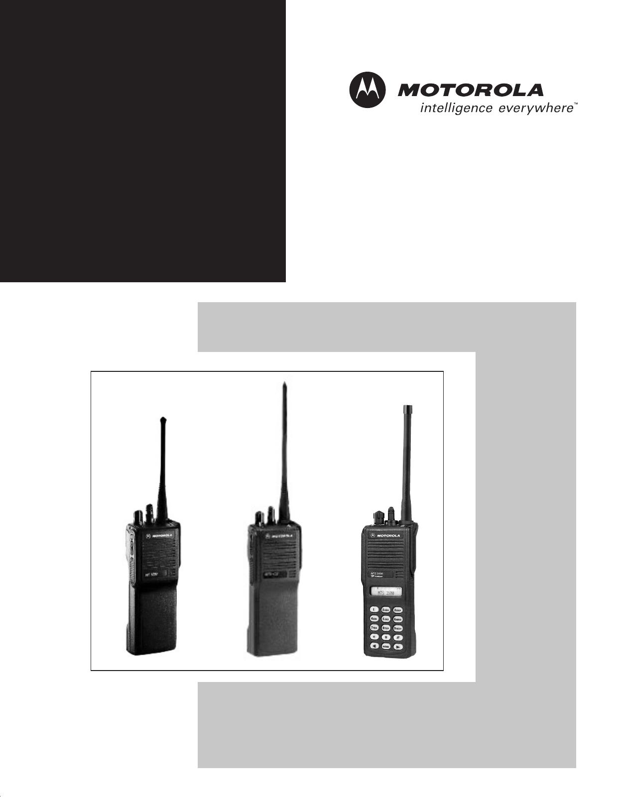
HT 1000
™
, MT 2000
™
,
MTS 2000
™
, and
MTX Series
Handie-Talkie
®
Portable Radios
Theory/Troubleshooting
Manual


HT 1000
TM
, MT 2000
TM
,
MTS 2000
TM
, and MTX Series
Handie-Talkie
®
Portable Radios
Theory/Troubleshooting Manual
Motorola
8000 West Sunrise Boulevard
Fort Lauderdale, Florida 33322
68P81200C15-O
Foreword
The information contained in this manual relates to all HT 1000™, MT 2000™, MTS 2000™, and MTX Series
Handie-Talkie
®
portable radios, unless otherwise specified.
For details on the operation of the radio, refer to the applicable manuals, which are available separately.
A list of related publications is provided in the section, “Related Publications Available Separately” on page iii.
Product Safety and RF Exposure Compliance
ATTENTION!
This radio is restricted to occupational use only to satisfy FCC RF energy exposure requirements.
Before using this product, read the RF energy awareness information and operating instructions in the
Product Safety and RF Exposure booklet enclosed with your radio (Motorola Publication part number
6881095C98) to ensure compliance with RF energy exposure limits.
For a list of Motorola-approved antennas, batteries, and other accessories, visit the following web site
which lists approved accessories: <http://www.motorola.com/cgiss/index.shtml>
Manual Revisions
Changes which occur after this manual is printed are described in FMRs (Florida Manual Revisions). These FMRs provide
complete replacement pages for all added, changed, and deleted items, including pertinent parts list data, schematics, and
component layout diagrams. To obtain FMRs, contact the Radio Parts Services Division.
Computer Software Copyrights
The Motorola products described in this manual may include copyrighted Motorola computer programs stored in
semiconductor memories or other media. Laws in the United States and other countries preserve for Motorola certain
exclusive rights for copyrighted computer programs, including, but not limited to, the exclusive right to copy or reproduce in
any form the copyrighted computer program. Accordingly, any copyrighted Motorola computer programs contained in the
Motorola products described in this manual may not be copied, reproduced, modified, reverse-engineered, or distributed in
any manner without the express written permission of Motorola. Furthermore, the purchase of Motorola products shall not
be deemed to grant either directly or by implication, estoppel, or otherwise, any license under the copyrights, patents or
patent applications of Motorola, except for the normal non-exclusive license to use that arises by operation of law in the
sale of a product.
Document Copyrights
No duplication or distribution of this document or any portion thereof shall take place without the express written permission
of Motorola. No part of this manual may be reproduced, distributed, or transmitted in any form or by any means, electronic
or mechanical, for any purpose without the express written permission of Motorola.
Disclaimer
The information in this document is carefully examined, and is believed to be entirely reliable. However, no responsibility is
assumed for inaccuracies. Furthermore, Motorola reserves the right to make changes to any products herein to improve
readability, function, or design. Motorola does not assume any liability arising out of the applications or use of any product
or circuit described herein; nor does it cover any license under its patent rights nor the rights of others.
Trademarks
MOTOROLA and the Stylized M logo are registered in the US Patent & Trademark Office. All other product or service
names are the property of their respective owners.
© Motorola, Inc. 2003.
Before using this product, read the operating instructions
for safe usage contained in the Product Safety and RF
Exposure booklet enclosed with your radio.
!
C a u t i o n
LIST OF TABLES...................................................................................................................................................
iii
LIST OF FIGURES.................................................................................................................................................
iii
RELATED PUBLICATIONS AVAILABLE SEPARATELY......................................................................................
iii
GLOSSARY OF TERMS........................................................................................................................................
iv
INTRODUCTION
I. PURPOSE .......................................................................................................................................................1
II. DESCRIPTION ................................................................................................................................................1
A. General......................................................................................................................................................1
B. Printed Circuit Boards and Flexible Circuits..............................................................................................1
THEORY OF OPERATION (BASIC FUNCTIONAL DESCRIPTION)
I. INTRODUCTION .............................................................................................................................................2
II. RADIO POWER...............................................................................................................................................2
A. General......................................................................................................................................................2
B. B+ Routing and DC Voltage Distribution (for a Closed Architecture Controller and a
VHF or UHF Transceiver) ...................................................................................................................2
C. B+ Routing and DC Voltage Distribution (for an Open Architecture Controller and an
800 or 900MHz Transceiver)...............................................................................................................2
III. VHF/UHF TRANSCEIVER BOARD.................................................................................................................4
A. Frequency Generation Unit (See Figure 2) ...............................................................................................4
B. Antenna Switch..........................................................................................................................................4
C. Receiver Front End (See Figure 3)............................................................................................................4
D. Receiver Back End (See Figure 3)............................................................................................................5
E. Transmitter (See Figure 4) ........................................................................................................................5
IV. 800/900MHz TRANSCEIVER BOARD ............................................................................................................6
A. Frequency Generation Unit (See Figure 5) ...............................................................................................6
B. Antenna Switch..........................................................................................................................................6
C. Receiver Front End (See Figure 6)............................................................................................................6
D. Receiver Back End (See Figure 6)............................................................................................................7
E. Transmitter (See Figure 7) ........................................................................................................................7
V. CLOSED ARCHITECTURE CONTROLLER ...................................................................................................8
A. General (See Figure 8)..............................................................................................................................8
B. Digital Architecture ....................................................................................................................................8
C. Audio Signalling Architecture.....................................................................................................................8
VI. OPEN ARCHITECTURE CONTROLLER........................................................................................................8
A. General (See Figure 9)................................................................................................................................8
B. Digital Architecture ....................................................................................................................................9
C. Audio Signalling Architecture.....................................................................................................................9
Theory/Troubleshooting Manual
6881200C15-A
HT 1000
TM
, MT 2000
TM
,
MTS 2000
TM
, and MTX Series
Handie-Talkie
®
Portable Radios
CONTENTS
TITLE PAGE
, Motorola, Handie-Talkie, HT 1000, MT 2000, MTS 2000, MTX 838, MTX 8000, MTX 9000, Private-Line, Digital Private-Line,
and Privacy Plus are trademarks of Motorola, Inc.
© 1993, 2003 by Motorola, Inc.
8000 W. Sunrise Blvd., Ft. Lauderdale, FL 33322
Printed in U.S.A. 7/03. All Rights Reserved.

ii
CONTENTS (cont.)
TITLE PAGE
THEORY OF OPERATION (DETAILED FUNCTIONAL DESCRIPTION)
I. INTRODUCTION ...........................................................................................................................................10
II. RADIO POWER.............................................................................................................................................10
A. General....................................................................................................................................................10
B. B+ Routing and DC Voltage Distribution (for a Closed Architecture Controller
and a VHF or UHF Transceiver) .......................................................................................................10
C. B+ Routing and DC Voltage Distribution (for an Open Architecture Controller
and an 800 or 900MHz Transceiver).................................................................................................11
III. VHF/UHF TRANSCEIVER.............................................................................................................................12
A. Frequency Generation Unit (FGU) ..........................................................................................................12
B. Antenna Switch........................................................................................................................................13
C. Receiver Front End..................................................................................................................................13
D. Receiver Back End..................................................................................................................................14
E. Transmitter ..............................................................................................................................................14
IV. 800/900MHz TRANSCEIVER BOARD ..........................................................................................................15
A. Frequency Synthesis...............................................................................................................................15
B. Antenna Switch........................................................................................................................................16
C. Receiver Front End..................................................................................................................................16
D. Receiver Back End..................................................................................................................................17
E. Transmitter ..............................................................................................................................................17
V. CLOSED ARCHITECTURE CONTROLLER .................................................................................................17
A. Microcomputer (U705).............................................................................................................................17
B. Controller Board Circuit Operation ..........................................................................................................19
VI. OPEN ARCHITECTURE CONTROLLER......................................................................................................21
A. Microprocessor (U705) and Associated Circuits .....................................................................................22
B. Controller Board Circuit Operation ..........................................................................................................24
VII. UNIVERSAL CONNECTOR (See Tables 2 and 3)........................................................................................28
TROUBLESHOOTING
I. INTRODUCTION ...........................................................................................................................................30
II. TROUBLESHOOTING PROCEDURE...........................................................................................................30
A. Check Batteries.......................................................................................................................................30
B. Alignment.................................................................................................................................................30
C. Check Overall Transmitter Operation......................................................................................................30
D. Check Overall Receiver Operation..........................................................................................................31
III. VOLTAGE MEASUREMENT AND SIGNAL TRACING.................................................................................31
IV. TROUBLESHOOTING CHARTS...................................................................................................................31
(VHF/UHF Transceiver/Closed Architecture Controller) ................................................................................32
(800/900MHz Transceiver/Open Architecture Controller)..............................................................................33
(VHF/UHF Transmitter RF)............................................................................................................................34
(800/900MHz Transmitter RF) .......................................................................................................................35
(VHF/UHF Receiver RF)................................................................................................................................36
(800/900MHz Receiver RF) ...........................................................................................................................37
(VHF/UHF DC Switch) ...................................................................................................................................38
(800/900MHz DC Switch) ..............................................................................................................................39
(VHF/UHF Frequency Generation Unit - FGU)..............................................................................................40
(800/900MHz Frequency Generation Unit - FGU) .........................................................................................41
(VHF/UHF Voltage Controlled Oscillator - VCO) ...........................................................................................42
(800/900MHz Voltage Controlled Oscillator - VCO).......................................................................................43
(VHF/UHF, Closed Architecture, No Receive Audio).....................................................................................44
(800/900MHz, Open Architecture, No Receive Audio) ..................................................................................45
(VHF/UHF, Closed Architecture, No Transmit Deviation)..............................................................................46
(800/900MHz, Open Architecture, No Transmit Deviation)............................................................................47
(Closed Architecture Controller).....................................................................................................................48
(Open Architecture Controller).......................................................................................................................49
(VHF/UHF Only, VCO Crossover Frequency Tune) ......................................................................................50

iii
TABLE TITLE PAGE
LIST OF TABLES
1 Option Select Definition...........................................................................................................18
2 Option Select Definition...........................................................................................................29
3 Universal Connector Mode......................................................................................................29
FIGURE TITLE PAGE
LIST OF FIGURES
1A DC Power Distribution Block Diagram
(Closed Architecture Controller and VHF or UHF Transceiver)..........................................3
1B DC Power Distribution Block Diagram
(Open Architecture Controller and 800 or 900MHz Transceiver)........................................3
2 VHF/UHF Frequency Generation Unit (FGU) Circuits...............................................................4
3 VHF/UHF Receiver Block Diagram...........................................................................................5
4 VHF/UHF Transmitter Block Diagram.......................................................................................5
5 800/900MHz Frequency Generation Unit (FGU) Circuits..........................................................6
6 800/900MHz Receiver Block Diagram ......................................................................................7
7 800/900MHz Transmitter Block Diagram ..................................................................................7
8 Closed Architecture Controller Block Diagram..........................................................................8
9 Open Architecture Controller Block Diagram ............................................................................9
RELATED PUBLICATIONS AVAILABLE SEPARATELY
Theory Manual (this publication)........................................................................................................68P81200C15
includes:
• theory of operation
• troubleshooting information and troubleshooting charts
Service Manual 68P81200C25
includes:
• all servicing information
• assembly / disassembly
• maintenance
Operating Instructions
• HT 1000 Portable Radios......................................................................................................68P81071C70
• MT 2000 Portable Radios .....................................................................................................68P81076C65
• MTS 2000 I Portable Radios................................................................................................68P81072C15
• MTS 2000 II and III Portable Radios...................................................................................68P81072C45
• MTX Series Model B3 Privacy Plus Portable Radios............................................................68P81072C10
• MTX Series Model B4 Privacy Plus Portable Radios............................................................68P81073C60
• MTX Series Model B5 and B7 Privacy Plus Portable Radios...............................................68P81072C40
Mobile Vehicular Adapter (MTVA) Operating Instructions..................................................................68P81075C85
Mobile Vehicular Adapter (MTVA) Installation Instructions................................................................68P81075C90
Remote Speaker Microphones Operating Instructions.......................................................................68P81073C40

ALC- Automatic Level Control; a circuit in the transmit RF path that controls RF power amplifier output, provides leveling over
frequency and voltage, and protects against high VSWR
ASF IC- Audio Signalling Filter Integrated Circuit
Closed architecture- A controller configuration that utilizes a microcomputer with internal ROM, RAM, and EEPROM
DTMF- Dual Tone Multi-frequency
DPL- Digital Private-Line™
Firmware- Software or a software/hardware combination of computer programs and data, with a fixed logic configuration
stored in a read-only memory; information can not be altered or reprogrammed
FGU- Frequency Generation Unit
FLASHport
™
- Is a Motorola term that describes the ability of a radio to change memory. Every FLASHport radio contains a
FLASHport EEPROM memory chip that can be software written and rewritten to, again and again.
ISW- Inbound Signalling Word; data transmitted on the control channel from a subscriber unit to the central control unit
LSH- Low Speed Handshake; 150 baud digital data sent to the radio during trunked operation while receiving audio
MDC- Motorola Digital Communications
MRTI- Motorola Radio-Telephone Interconnect; a system that provides a repeater connection to the Public Switched
Telephone Network (PSTN). The MRTI allows the radio to access the telephone network when the proper access code is
received.
MSK- Minimum-Shift Keying
OMPAC- Over-Molded Pad-Array Carrier; a Motorola custom package, distinguished by the presence of solder balls on the
bottom pads
Open architecture- A controller configuration that utilizes a microprocessor with extended ROM, RAM, and EEPROM
OSW- Outbound Signalling Word; data transmitted on the control channel from the central controller to the subscriber unit
PC Board- Printed Circuit Board
PL- Private-Line
®
tone squelch; a continuous sub-audible tone that is transmitted along with the carrier
PLL- Phase-Locked Loop; a circuit in which an oscillator is kept in phase with a reference, usually after passing through a
frequency divider
PTT- Push-To-Talk; the switch located on the left side of the radio which, when pressed, causes the radio to transmit
Registers- Short-term data-storage circuits within the microcontroller
Repeater- Remote transmit/receive facility that re-transmits received signals in order to improve communications coverage
RESET- Reset line; an input to the microcontroller that restarts execution
RF PA- Radio Frequency Power Amplifier
RSSI- Received Signal Strength Indicator; a dc voltage proportional to the received RF signal strength
RPT/TA- Repeater/Talk-Around
RX DATA- Recovered digital data line
SCI IN- Serial Communication Interface Input line
SLIC- Support-Logic IC; a custom gate array used to provide I/O and memory expansion for the microprocessor
Softpot- Software potentiometer; a computer-adjustable electronic attenuator
Software- computer programs, procedures, rules, documentation, and data pertaining to the operation of a system
SPI (clock and data lines)- Serial Peripheral Interface; how the microcontroller communicates to modules and ICs through
the CLOCK and DATA lines
Squelch- Muting of audio circuits when received signal levels fall below a pre-determined value
SRAM- Static-RAM chip used for scratch-pad memory
Standby mode- An operating mode whereby the radio is muted but still continues to receive data
System central controller- Main control unit of the trunked dispatch system; handles ISW and OSW messages to and from
subscriber units (see ISW and OSW)
System select- The act of selecting the desired operating system with the system-select switch (also, the name given to this
switch)
TOT- Time-Out Timer; a timer that limits the length of a transmission
TSOP- Thin Small-Outline Package
µC- Microcomputer
µP- Microprocessor
VCO- Voltage-Controlled Oscillator; an oscillator whereby the frequency of oscillation can be varied by changing a control
voltage
VCOB IC- Voltage-Controlled Oscillator Buffer Integrated Circuit
VSWR- Voltage Standing Wave Ratio
iv
GLOSSARY OF TERMS

I. PURPOSE
This manual will provide a theoretical explanation of
the HT 1000, MT 2000, MTS 2000, and MTX Series
portable radio’s operation, troubleshooting, and addition-
al useful information about the radio not found in
any other publication. The manual is divided into three
sections:
• INTRODUCTION
• THEORY OF OPERATION
• TROUBLESHOOTING
In the THEORY OF OPERATION section, a basic
functional description is followed with a more detailed
description of some selected circuits. All applicable fre-
quency bands are covered in this publication.
A complete list of models and each model’s descrip-
tion is provided in a separate service manual. A detailed
description of the radio’s operational features, a list of
applicable batteries and accessories, and a section on
general radio information is provided in several operat-
ing instruction manuals. To help you with your selection,
a complete list of the other publications on HT 1000, MT
2000, MTS 2000, and MTX Series portable radios can
be found following the Table of Contents of this manual.
II. DESCRIPTION
A. General
The HT 1000 Handie-Talkie portable radio is a
microcomputer-based, single-mode (conventional)
transceiver. The MT 2000, MTS 2000, and MTX Series
Handie-Talkie portable radios are microprocessor-based
dual-mode (trunked/conventional) transceivers. In all of
the radios, the microcomputer determines the active
state of the radio (transmit/receive), monitors radio sta-
tus, and processes operator commands entered from
the keypad (if applicable) or the other radio controls.
Various switches, buttons, knobs, and indicators are
ergonomically designed, making placement in strategic
locations on the different model radios. Refer to the spe-
cific operating instructions on your radio for location and
description of these controls. All of the controls, includ-
ing the push-to-talk (PTT) switch and key pad
(if applicable) are weather resistant. The microphone
and speaker are covered by a diaphragm for additional
protection.
B. Printed Circuit Boards and Flexible Circuits
Most of the radio circuitry is contained in chip carri-
ers that are mounted on one of the two rigid, printed
circuit boards (PC boards); the controller board and the
transceiver board. Front display model radios contain a
third rigid PC Board; the keypad/display board, which is
a two-sided board supporting the DTMF keypad, and a
14-character, dot-matrix display. This board is not field
serviceable. If a fault develops with the keypad, display,
or backlights, the entire board must be replaced. Also,
the top-display model radios contain a small display
board located under the top escutcheon. This provides
2-character, 6-segment, starburst-type display. This
board is not field serviceable. The entire board must be
replaced.
All discrete wiring has been replaced with flexible
circuits: a controls flex, a front cover/display flex, and a
jumper flex. The controls flex interconnects the top con-
trols and the side controls (PTT switch, emergency push
button, telephone-interconnect push button) with the
controller board. The front cover/display flex routes sig-
nals between the controller, the 13-pin universal
connector, the front cover components (speaker and
microphone), and if applicable, the display/keypad
board. The jumper flex routes signals between the
transceiver and the controller board.
1
INTRODUCTION

I. INTRODUCTION
This publication covers a large family of portable
radios: HT 1000, MT 2000, MTS 2000, and MTX series
units. They are software driven, and because of the
wide range of operating systems and radio functionality
provided by this family of radios, the theory discussions
will be divided into several major categories. The
transceiver is frequency sensitive and falls into one of
four frequency bands: vhf, uhf, 800MHz, or 900MHz.
Because of their similarity, transceivers will be catego-
rized into two discussion groups: vhf/uhf transceivers
and 800/900MHz transceivers. The controller falls into
two categories: a closed architecture controller and an
open architecture controller. Each controller will be dis-
cussed separately. This THEORY OF OPERATION
section of the manual provides a functional description
of the radio. First, overall radio functions are discussed
in basic terms, with each circuit and its relationship to
other parts of the radio described. Then, a more detailed
functional description is given for circuit relationships,
with special attention directed to some of the selected
circuits. Pay particular attention to the topics being dis-
cussed, and note the application: vhf/uhf transceiver,
open architecture controller, etc.
II. RADIO POWER
A. General
In this family of radios, power is distributed to four
general combinations of transmitters and controllers:
1. vhf/uhf xcvr with closed architecture controller
2. vhf/uhf xcvr with open architecture controller
3. 800/900MHz xcvr with closed architecture controller
4. 800/900MHz xcvr with open architecture controller
Discussing each of the four combinations would be
somewhat redundant, so pairs 1 and 4 were chosen for
illustration and explanation in the following paragraphs.
Paragraph B covers the vhf/uhf transceiver and the
closed architecture controller; paragraph C covers the
800/900MHz transceiver and the open architecture con-
troller.
B. B+ Routing and DC Voltage Distribution
(for a Closed Architecture Controller and a
VHF or UHF Transceiver)
Operating power for the radio is derived from a 7.5-
volt battery (BATT 7.5V), which is applied directly to the
transceiver board as B+. The B+ voltage is fused and
routed through the jumper flex as Raw B+ and applied
through the controller board to the controls flex. In the
controls flex, B+ is applied to the on/off/volume control.
When the radio is turned on, switched B+ (SB+) and the
voltage sources required to operate various stages of
the radio are distributed as shown in Figure1A.
The power amplifier (PA) module (U105) and auto-
matic level control (ALC) IC (U101) of the RF board are
powered-up directly from the BATT B+. Other sections
of the transceiver board are powered-up through the
switched B+. Two 5-volt regulators are used on the
transceiver board; one 5V regulator (U202) is used to
supply those circuits which require voltages to be on all
the time, such as the reference oscillator, synthesizer
IC, IF IC, and digital-to-analog (D/A) IC. The voltage-
control oscillator (VCO) buffer obtains its voltage (Vcc)
from the SOUT line of the synthesizer. The other 5V
regulator (U103) of the transceiver board supplies 5V to
the receiver RF AMP IC and Mixer IC during the receive
mode and to the ALC and other transmitter circuitry dur-
ing the transmit mode.
The controller board obtains its voltage source from
switched B+, and produces regulated 5 volts from two
regulators. One 5V regulator (U709) is used to supply
5V to the microcomputer. The SB+ is also connected to
the AUDIO PA. The audio signalling filter (ASF) IC
obtains its 5V (Vcc) from the AUDIO PA (U706) internal
5V regulator.
C. B+ Routing and DC Voltage Distribution
(for an Open Architecture Controller and an
800 or 900MHz Transceiver)
Refer to figure 1B and note that operating power for
the radio is derived from a 7.5-volt battery (BATT 7.5V),
which is applied directly to the transceiver board as B+.
The B+ voltage is fused and routed through the jumper
flex as Raw B+ and applied to the controller board.
From the controller, B+ is applied to three different
areas:
1. the expansion board, via connector jack J702 pin1,
2. an electrical switch IC, U712 pins 2 and 3, and
3. the controls flex, via connector jack J703 pin 8.
The UNSW B+ is routed to the expansion board so
that functions there can be performed independently of
the SW B+ supply. The UNSW B+ is also routed to the
electrical switch IC, U712 (a P-channel FET in an SOIC-
8 package), which connects it to SW B+ when the
control voltage at U712 pin 4 is low. The SW B+ is then
distributed to the rest of the radio, including the
transceiver board, front cover/display flex, and expan-
sion board, as well as other controller board circuitry.
Finally, UNSW B+ is routed to the mechanical on/off
switch and returns to the controller as MECH SWB+.
The MECH SWB+ signal activates the electrical switch
(U712), and also feeds a resistive divider so that the
microprocessor (U705) can monitor the battery voltage.
2
THEORY OF OPERATION (BASIC FUNCTIONAL DESCRIPTION)
3
5V
Regulator
U709
U705
Micro C
ASF IC
U701
U706
Audio PA
5V
SB+
Controller Board
Battery
7.5V
+
B+
PA Module
5V
Regulator
VCOB IC
ALC
T5
L105
CR108
RX
L122
L121
Vcc
U105
U202
T5
U201
U101
Harmonic
Filter
RF Amp
Mixer
Q107
R5
Q105
5V
5V
Regulator
U103
R/T
SB+
Synth
Ref Osc
IF IC
D/A IC
Transceiver Board
CR109
5V
S
Out
Fuse
1 Amp
Universal Connector
Front Cover
Flex
Jumper Flex
Controls
Flex
Opt B+
SB+
SB+
SB+
Raw B+
B+
SB+
On
Off
5V
5V
Regulator
U709
U705
Micro P
ASF IC
U701
U706
Audio PA
5V
SB+
Controller Board
Battery
7.5V
+
PA Module
5V
Regulator
VCOB IC
L105
CR108
Vss
U105
U202
T5
U101
RF Amp
Mixer
R5
Synth
Ref Osc
IF IC
D/A IC
Transceiver Board
CR109
5V
S
Out
Fuse
1 Amp
Universal Connector
Front Cover
Flex
Jumper Flex
Controls
Flex
Opt B+
SB+
SB+
Raw B+
Raw B+
MECH SB+
On
Off
ALC
FLASH
EEPROM
SLIC
SRAM
HEAR/
CLEAR
*U601
Q702
SB+
U712
Electrical
Switch
Expansion
Board
Q101
VCO
T5
Q108
C138
R5
RX
Q703
* U601 HEAR/CLEAR used on 900 MHz radios only.
BATT B+
B+ CNTL
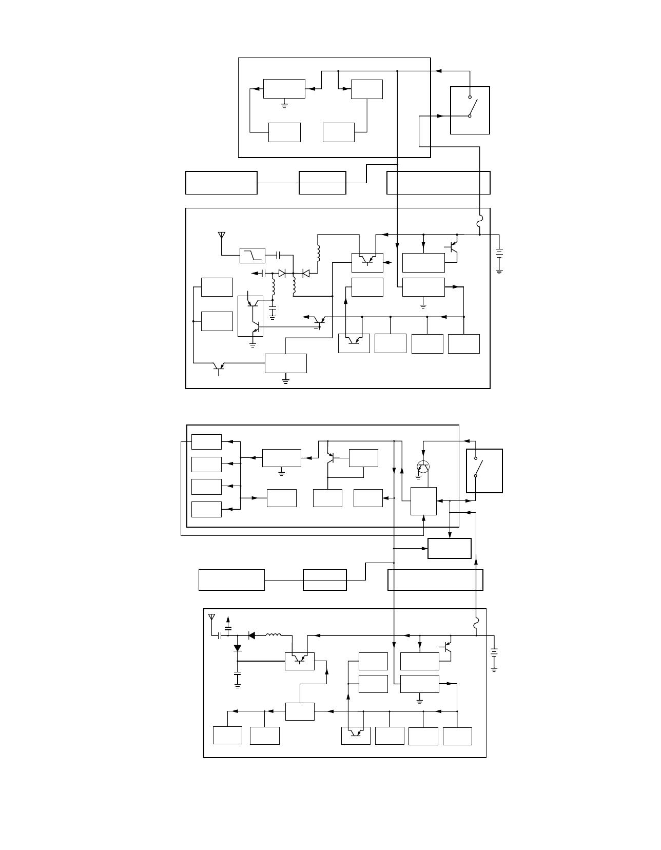
Figure 1A. DC Power Distribution Block Diagram (Closed Architecture Controller and VHF or UHF Transceiver)
Figure 1B. DC Power Distribution Block Diagram (Open Architecture Controller and 800 or 900MHz Transceiver)
In the transceiver, SWB+ is routed directly to the 5v
regulator (U202). The regulated 5v supplies the IF IC
(U3), the reference oscillator (U203), the Fractional-N
synthesizer IC (U204), the D/A IC (U102), and the R/T
switch (Q108).
Internal to the synthesizer is a superfilter which sup-
plies the VCO module (U205) and the VCO buffer IC
(U201) with 4.6 volts, produced by the regulated 5V
supply.
In addition, two more 5-volt supplies exist, one for
transmit and one for receive: T5 and R5, respectively.
The regulated 5v is switched to either one or the other
by transistor Q108, under the control of the D/A IC. The
T5 voltage is used as a control line by the TX ALC IC
and provides bias for the RF PA input and the external
antenna connector. The R5 voltage is supplied to the
RF amplifier (U1) and the Mixer Buffer IC (U2).
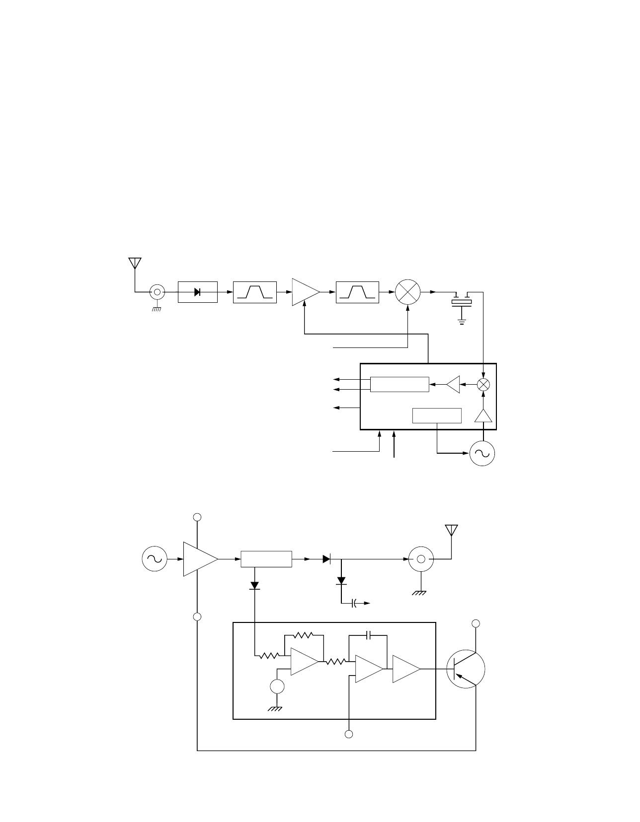
III. VHF/UHF TRANSCEIVER BOARD
A. Frequency Generation Unit (See Figure 2)
The frequency generation unit (FGU) consists of
three major sections: the high stability reference oscilla-
tor(U203), fractional-N synthesizer (U204), and VCO
buffer IC(U201). The VCO provides the carrier frequen-
cy for the transmitter (TX OUT), and provides the local
oscillator (LO) injection signal for the receiver mixer
buffer (RX OUT).
The RX VCO uses an external active device, where-
as the TX VCO uses the internal device of the VCO
buffer IC. The phase lock loop (PLL) circuit is provided
by the fractional-N synthesizer IC.
The output of the VCO is amplified by the prescaler
buffer, routed through a low-pass filter, and applied to
the prescaler divider of the synthesizer. The divide ratios
are determined from information stored in memory that
was bussed to the synthesizer via the microcomputer.
The microcomputer extracts data for the division ratio as
determined by the channel select switch. The resultant
VCO buffer signal is applied to a comparator in the syn-
thesizer. The synthesizer comparator also receives a
reference frequency via a reference divider input from
the 16.8 MHz temperature-compensated reference
oscillator. If the two frequencies differ, the synthesizer
generates a control (error) voltage which causes the
VCO to change frequency.
Modulation of the carrier is achieved by using a 2-
port modulation technique. The deviation of the low
frequency tone, such as DPL/TPL, is achieved by inject-
ing the signal to an analog/digital circuit in the
synthesizer. The resultant digitized signal is then modu-
lated by the fractional N-divider, thus generating the
required deviation. The deviation of the high frequency
tone is achieved by modulating the modulation varactor
on the VCO. In order to cover a very wide bandwidth,
the VCO control voltage is stepped up by using a posi-
tive and negative multiplier circuit. A 13-volt supply
powers the phase detector circuitry. The VCO signal is
amplified by the integrated buffer amplifier of the VCO
buffer. The two output signals, receiver first LO injection
and transmitter carrier frequency, are filtered and then
routed to the mixer/buffer (U2) and the RF PA (U105),
respectively.
B. Antenna Switch
The function of the antenna switch is to route the
transmitter power to the antenna during the transmit
mode, or route RF from the antenna to the receiver front
end during the receive mode.
C. Receiver Front End (See Figure 3)
The RF signal from the antenna is coupled to the
first bandpass filter through the antenna switch. The out-
put of the bandpass filter is then applied to a wideband
RF amplifier IC (RF AMP). The bandpass filter is elec-
tronically tuned by the D/A IC, which is controlled by the
microcomputer. Wideband operation of the filter is
achieved by retuning the bandpass filter across the
band. After amplification, the RF signal is further filtered
by a second fixed-tuned filter to improve the spurious
rejection.
4
Negative Multiplier
Positive Multiplier
Counter for
Multiplier
Fractional
Divider
Pre-scaler
Divider
A/D
Fractional-N
Synthesizer
Loop
Filter
Low Pass Filter
16.8 MHz
Ref Osc
Modulating
Signal
2.1/2.4 MHz
Reference
Clock to
ASFIC
Mod Out
RX VCO
TX VCO
Prescaler
Buffer
TX Buffer
RX Buffer
Switching CCTS
for VCO and Buffer
U201
VCO Buffer IC
Low Pass
Filter
Matching
CCT
Mixer/Buffer
RF PA Input
U204
RX Out
TX Out
Reference
Divider
Figure 2. VHF/UHF Frequency Generation Unit (FGU) Circuits
MAEPF-23266-O
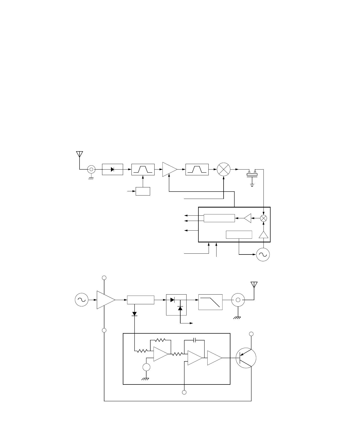
The filtered RF signal is then applied to the RF input
of a broadband mixer IC. An injection signal (FIRST
LO), supplied by the FGU, is applied to the second input
of the mixer stage. The resulting difference frequency
(44.85MHz for VHF and 73.35MHz for UHF), is the first
IF frequency. The first IF frequency is then filtered by a
2-pole crystal filter to remove unwanted mixer products
and routed to the IF IC.
D. Receiver Back End (See Figure 3)
In the IF IC, the first IF frequency is down convert-
ed, amplified, filtered, and demodulated to produce the
recovered audio. The IF IC is electronically pro-
grammable, and the amount of filtering, which is
dependent on the radio channel spacing, is controlled
by the microcomputer. Additional filtering, which used to
be provided externally by a conventional ceramic filter,
is replaced by internal filters in the IF IC. The IF IC uses
a type of direct conversion process where the second
LO frequency is very close to the first IF frequency. The
IF IC controls the second LO VCO and causes the VCO
to track the first IF frequency, producing a phase-locked
operation. The IF IC also provides a recovered signal-
strength indicator (RSSI) and squelch output for use in
other parts of the radio.
E. Transmitter (See Figure 4)
The transmitter consists of the following stages:
• Harmonic Filter
• RF Power Amplifier
• ALC IC, which controls the power output
Harmonics of the carrier frequency are generated
by the PA module and antenna switch. The harmonic fil-
ter circuit attenuates the unwanted signals.
5
Antenna
Pin Diode
Antenna
Switch
Varactor
Tuned Filter
RF Amp
Fixed Tuned
Filter
AGC
D/A
SPI Bus
First LO
From FGU
Recovered Audio
Squelch
RSSI
16.8 MHz
Reference Clock
Demodulator
I-F IC
SPI Bus
Synthesizer
Second
LO VCO
Crystal
Filter
Mixer
RF Jack
MAEPF-23265-O
Figure 3. VHF/UHF Receiver Block Diagram
Figure 4. VHF/UHF Transmitter Block Diagram
V Supply
Pin Diode
Antenna
Switch
Coupler
RF PA
VCO
Synthesizer
To Receiver
Front End
Antenna
RF Jack
Harmonic
Filter
V Control
V Det
B+
V Ref
V
ALC IC
Batt B+
MAEPF-23264-O
The RF PA module is a multi-stage amplifier, which
has the required gain to produce an output level of sev-
eral watts. Some harmonic filtering is accomplished in
the RF PA.
Power control is achieved by using the coupler
detector to feed back a portion of the PA output to the
ALC circuit. This ALC circuit increases or decreases the
overall PA gain as appropriate. Another function of the
detector is to provide a signal when the VSWR exceeds
the threshold level. This signal, combined with the
forward detected power, is used to reduce the PA output
power, thus protecting the PA under high VSWR
conditions.
IV. 800/900MHz TRANSCEIVER BOARD
A. Frequency Generation Unit (See Figure 5)
The frequency generation unit (FGU) consists of the
following major sections: the high stability reference
oscillator (U203), fractional-N synthesizer (U204), VCO
buffer IC (U201), and VCO (U205). The VCO provides
the carrier frequency for the transmitter (TX OUT), and
provides the local oscillator (LO) injection signal for the
receiver mixer buffer (RX OUT). The phase lock loop
(PLL) circuit is provided by the fractional-N synthesizer
IC.
The output of the VCO is amplified by the prescaler
buffer, routed through a low-pass filter, and applied to
the prescaler dividers of the synthesizer. The divide
ratios are determined from information stored in memory
that is bussed to the synthesizer via the microprocessor.
The microprocessor extracts data for the division ratio
as determined by the channel-select switch. The resul-
tant VCO buffer signal is applied to a comparator in the
synthesizer. The synthesizer comparator also receives a
reference frequency via a reference divider input from
the 16.8 MHz temperature-compensated reference
oscillator. If the two frequencies differ, the synthesizer
generates a control (error) voltage which causes the
VCO to change frequency.
Modulation of the carrier is achieved by using a 2-
port modulation technique. The deviation of the low
frequency tone, such as DPL/TPL, is achieved by inject-
ing the signal to an analog/digital circuit in the
synthesizer. The resultant digitized signal is then modu-
lated by the fractional N-divider, thus generating the
required deviation. The deviation of the high frequency
tone is achieved by modulating the modulation varactor
on the VCO. In order to cover a very wide bandwidth,
the VCO control voltage is stepped up by using a posi-
tive multiplier circuit. A 13-volt supply powers the phase
detector circuitry. The VCO signal is amplified by the
integrated buffer amplifier of the VCO buffer. The two
output signals, receiver first LO injection and transmitter
carrier frequency, are filtered and then routed to the
mixer/buffer (U2) and the RF PA (U105), respectively.
B. Antenna Switch
The function of the antenna switch is to route the
transmitter power to the antenna during the transmit
mode, or route the RF from the antenna, to the receiver
front end during the receive mode.
C. Receiver Front End (See Figure 6)
The RF signal from the antenna is coupled to the
first bandpass filter through the antenna switch. The out-
put of the bandpass filter is then applied to a wideband
RF amplifier IC (RF AMP). The bandpass filter is a wide-
band stripline filter, which is pretuned for the frequency
band. After amplification, the RF signal is further filtered
by a second fixed-tuned stripline filter to improve the
spurious rejection.
The filtered RF signal is then applied to the RF input
of a broadband mixer IC, U2. An injection signal (FIRST
LO) supplied by the FGU, is applied to the second input
of the mixer stage. The resulting difference frequency of
73.35MHz is the first IF frequency. The first IF frequency
is then filtered by a 2-pole crystal filter, FL1, to remove
unwanted mixer products and routed to the IF IC, U3
6
Positive Multiplier
Reference
Divider
Counter for
Multiplier
Fractional
Divider
Pre-scaler
Divider
A/D
Fractional-N
Synthesizer
Loop
Filter
Low Pass Filter
16.8 MHz
Ref Osc
Modulating
Signal
2.1/2.4 MHz
Reference
Clock to
ASFIC
Mod Out
RX VCO
TX VCO
Prescaler
Buffer
TX Buffer
RX Buffer
Switching CCTS
for VCO and Buffer
U201
VCO Buffer IC
Low Pass
Filter
Matching
CCT
Mixer/Buffer
RF PA Input
U204
RX Out
TX Out
To
I-F IC
MAEPF-23421-O
Figure 5. 800/900MHz Frequency Generation Unit (FGU) Circuits
D. Receiver Back End (See Figure 6)
In the IF IC, the first IF frequency is down convert-
ed, amplified, filtered, and demodulated to produce the
recovered audio. The IF IC is electronically pro-
grammable, and the amount of filtering, which is
dependent on the radio channel spacing, is controlled
by the microprocessor. Filtering is accomplished by
internal filters in the IF IC. The IF IC uses a type of
direct conversion process where the second LO fre-
quency is very close to the first IF frequency. The IF IC
controls the second LO VCO and causes the VCO to
track the first IF frequency, producing a phase-locked
operation. The IF IC also provides a recovered signal-
strength indicator (RSSI) and squelch output for use in
other parts of the radio.
E. Transmitter (See Figure 7)
The transmitter consists of the following stages:
• Low-pass antenna matching circuit
• RF Power Amplifier
• ALC IC and coupler, for power output control
The low-pass antenna matching circuit attenuates
RF PA harmonics, and provides the optimum phase
load to the RF PA. The RF PA module is a multi-stage
amplifier, which has the required gain to produce an out-
put level of several watts. Some harmonic filtering is
also accomplished in the RF PA.
Power control is achieved by using the coupler
detector to feed back a portion of the PA output to the
ALC circuit. This ALC circuit increases or decreases the
7
Antenna
Pin Diode
Antenna
Switch
Stripline
Filter
RF Amp
Stripline
Filter
AGC
First LO
From FGU
Recovered Audio
Squelch
RSSI
16.8 MHz
Reference Clock
Demodulator
IF IC
SPI Bus
Synthesizer
Second
LO VCO
Crystal
Filter
Mixer
RF Jack
Figure 6. 800/900MHz Receiver Block Diagram
MAEPF-23420-O
V Supply
Pin Diodes
Antenna
Switch
Coupler
RF PA
VCO
Synthesizer
To Receiver
Front End
Antenna
RF Jack
V Control
V Det
B+
V Ref
V
ALC IC
Batt B+
Ref.
Figure 7. 800/900MHz Transmitter Block Diagram
MAEPF-23419-O
overall PA gain as appropriate. Another function of the
detector is to provide a signal when the VSWR exceeds
the threshold level. This signal, combined with the
forward detected power, is used to reduce the PA output
power, thus protecting the PA under high VSWR
conditions.
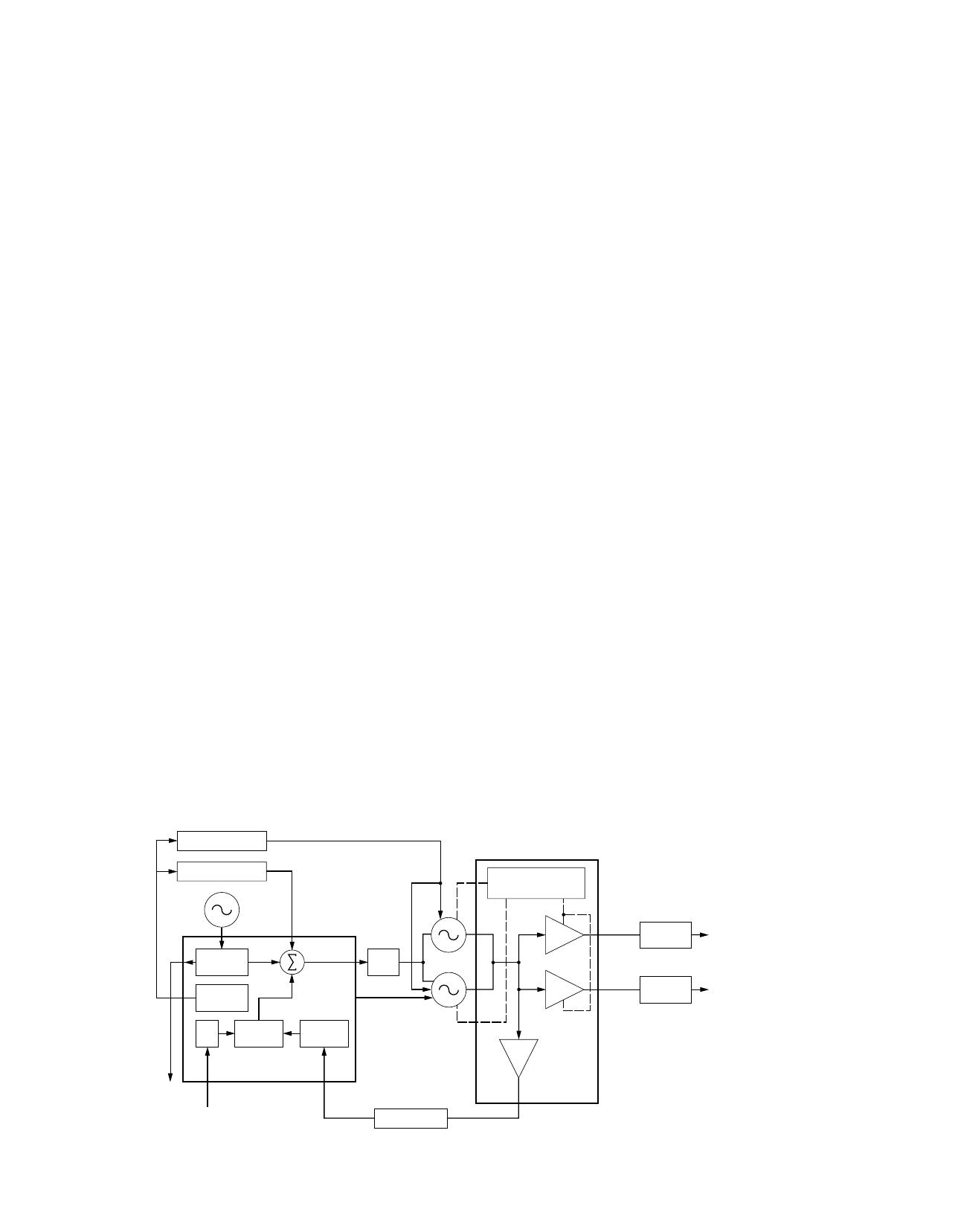
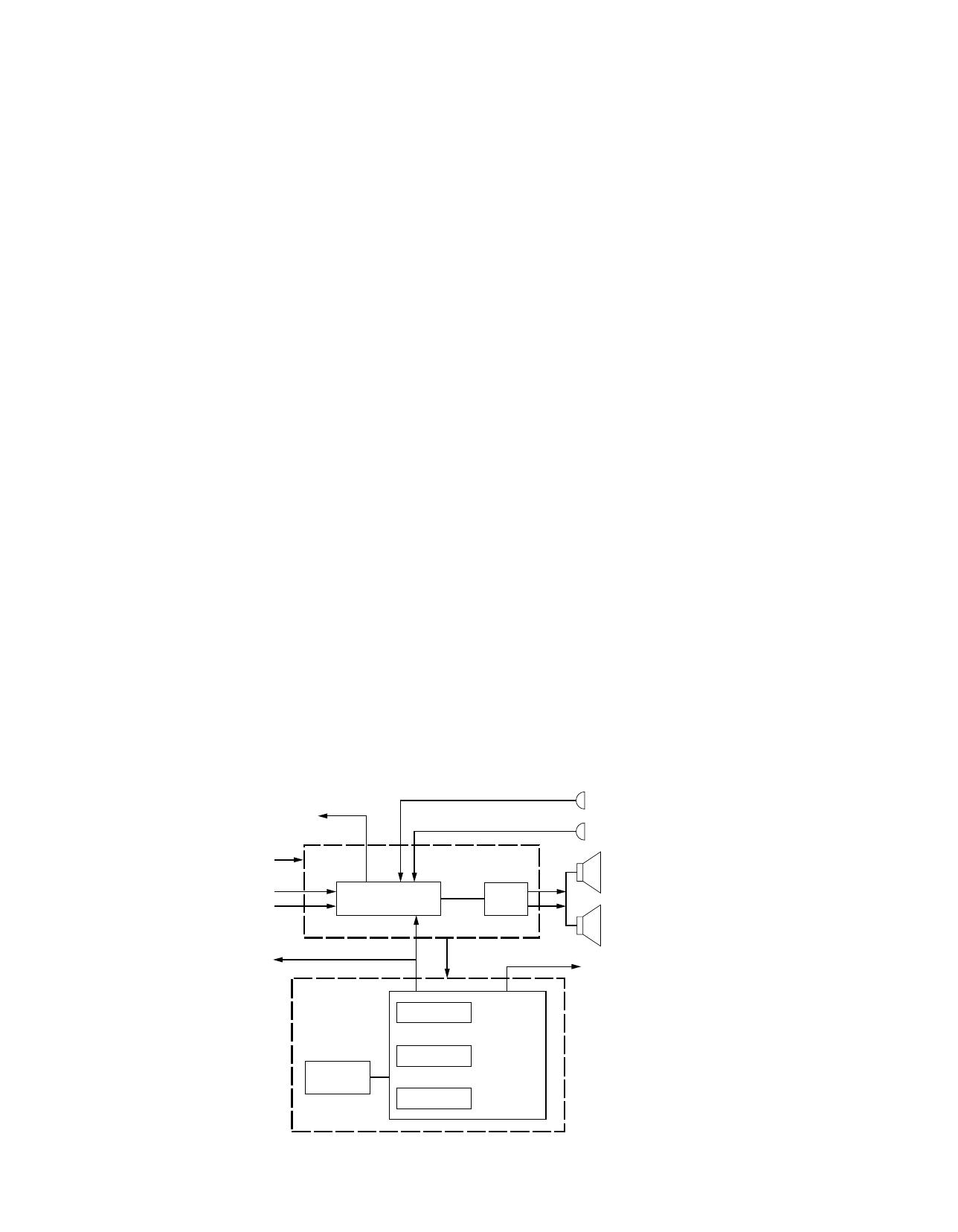
V. CLOSED ARCHITECTURE CONTROLLER
A. General (See Figure 8)
The controller board is the central interface between
various subsystems of the radio. It is segregated into
digital and audio architecture. The digital portion con-
sists of a special Motorola microcomputer. The audio
power amplifier (AUDIO PA) and audio/signalling/filter
IC (ASF IC) form the backbone of the audio/signalling
architecture. The controller board has its own voltage
regulators to generate 5 volts, sourced by switched B+
from the battery.
B. Digital Architecture
The Motorola microcomputer consists of 640 bytes
of EEPROM, 760 bytes of RAM, and 24k of ROM. The
microcomputer executes the radio software and moni-
tors the activity of all user interfaces. Using the
communication buses, the microcomputer handles the
responsibility of programming all applicable ICs in the
radio, including those on the RF transceiver board. This
programming sets up the ICs to properly perform a vari-
ety of functions, such as what frequency to transmit or
what channels to scan. The digital circuitry is powered
by a discrete 5-volt regulator to help isolate the digital
signals from the audio signals in nearby circuits.
C. Audio Signalling Architecture
A Motorola custom IC (ASF) provides both transmit
and receive audio and signalling processing. The ASF
IC is programmable by the microcomputer via the serial
peripheral interface (SPI). It provides filtering on both
transmit and receive audio, and also provides PL, DPL,
and MDC encoding and decoding.
In the transmit mode, the ASF IC amplifies, shapes,
limits, and filters the outgoing signal. The processed sig-
nal is sent to the transceiver board’s FGU. In the receive
mode, the demodulated signal from the receiver back
end is amplified, filtered and routed to the AUDIO PA for
amplification. The ASF IC provides pre-emphasis and
de-emphasis as well as squelch. Based on a reference
signal from the transceiver board, the ASF IC provides
the microcomputer with a clock signal.
Received audio signal amplification is achieved by
the AUDIO PA IC. The IC’s output drives the radio’s
internal speaker, or an external speaker connected via
an option cable. In order to minimize the effects, and to
further isolate the audio signals from the digital signals,
the audio section has its own isolated 5V regulator on
the AUDIO PA.
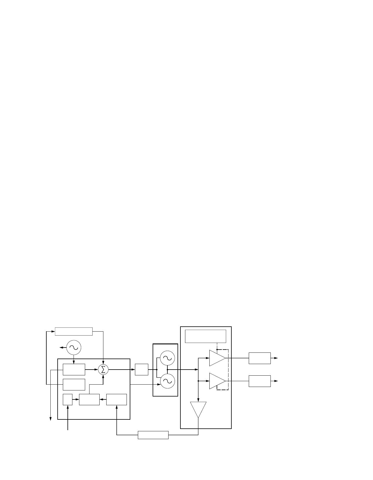
VI. OPEN ARCHITECTURE CONTROLLER
A. General (See Figure 9)
The controller board is the central interface between
various subsystems of the radio. The controller board is
composed of both digital and audio circuits. The digital
portion consists of a special Motorola microprocessor
(U705), a custom, gate-array, memory-support-logic IC
(SLIC), U710, and the memory devices (U713, U714,
and U715). The audio circuits include the audio power
amplifier (U702), the audio/signalling/filter IC (ASF IC),
U701, and in the 900MHz radios, the Hear Clear IC,
U601. The controller board has its own voltage regula-
tors to generate 5 volts, sourced by switched B+ from
the battery. The open architecture controller board also
has a plug-in interface for secure voice encryption
options, and another interface for the display and key-
pad version radios.
8
TO FGU
MOD
Out
2.1/2.4 MHz
Reference Clock
From FGU
Recovered Audio
Squelch
To RF Board
SPI
Audio Filter and
Signalling IC
Audio/Signalling
Architecture
Audio
PA
uP Clock
SCI to Side
Connector
Internal
Speaker
External
Speaker
Internal
Microphone
External
Microphone
HC11K4
768 RAM
640 EEPROM
24K ROM
5V
Regulator
Digital
Architecture
MAEPF-23267-O
Figure 8. Closed Architecture Controller Block Diagram

B. Digital Architecture
The Motorola microprocessor, in conjunction with
the SLIC, performs the functions of controlling the inter-
nal workings of the radio, as well as interfacing with the
outside world. The microprocessor has 1K of RAM and
512 bytes of EEPROM on the chip. In some versions
the controller board enhances the capabilities of the
microprocessor chip by providing 256K or 512K of
FLASH memory, 32K static RAM, and 8K or 32K of
EEPROM. Other versions use masked programmed
ROM.
The “FLASH” open controller is flexible and capable
of firmware being reprogrammed to support future fea-
tures. The controller, through communication busses,
programs all applicable ICs in the radio (including those
on the transceiver board) for proper operation in the
designated frequency band.
C. Audio Signalling Architecture
The Motorola custom integrated circuit, ASF IC, per-
forms audio signal shaping and filtering. The ASF IC
also encodes and decodes Private-Line (PL), Digital Pri-
vate-Line (DPL), and Motorola Digital Communication
(MDC) signals, as well as decoding trunking signals.
In the transmit mode, the ASF IC amplifies and
shapes the modulating signal on its way to the modulat-
ing port of the FGU. In the receive mode, the ASF IC
amplifies and filters the demodulated signal and applies
it to the audio PA, which drives the internal or external
radio speaker. The ASF IC not only performs pre-
emphasis and de-emphasis, but also performs the
squelch functions and provides the microprocessor with
a clock signal.
9
Expander
Compressor
Flutter
Filter
Squelch
To Receiver
Board
Recovered
Audio
Mod Out
SPI
To FGU
2.1/2.4 MHz
REF Clock
From FGU
*U601
HEAR/CLEAR
U702
Audio
PA
External
Microphone
Internal
Microphone
External
Speaker
Internal
Speaker
EEPROM
SRAM
Digital
Architecture
U705
MCII FI
u Processor
U710
SLIC
Masked ROM
or
FLASH
SCI
To Universal
Connector
uP
Clock
U701
ASF IC
* U601 HEAR/CLEAR used on 900 MHz radios only.
Audio/
Signalling
Architecture
MAEPF-23422-O
Figure 9. Open Architecture Controller Block Diagram

I. INTRODUCTION
In this section of the of the manual, a more detailed
description of the radio and some special circuit is given.
For a better understanding of the circuits descriptions,
and to aid in following the text, refer to the applicable
schematic diagram(s) in the corresponding service man-
ual (Motorola part number 68P81200C25), or previously
68P81200C20.
II. RADIO POWER
A. General
As previously described in the THEORY OF OPER-
ATION (BASIC FUNCTIONAL DESCRIPTION) RADIO
POWER paragraph, power is distributed to four general
combinations of transmitters and controllers:
1. VHF/UHF transceiver with closed architecture
controller,
2. VHF/UHF transceiver with open architecture
controller,
3. 800/900MHz transceiver with closed architecture
controller, and
4. 800/900MHz transceiver with open architecture
controller
Discussing each of the four combinations would be
somewhat redundant, so pairs 1 and 4 were chosen for
explanation in the following paragraphs. Paragraph B
covers the vhf/uhf transceiver and the closed architec-
ture controller; paragraph C covers the 800/900MHz
transceiver and the open architecture controller.
B. B+ Routing and DC Voltage Distribution
(for a Closed Architecture Controller and a
VHF or UHF Transceiver)
Raw B+ (7.5V) from the battery (Batt B+) enters the
radio on the transceiver board through a 3-contact
spring pin arrangement (P404) as B+, where it is routed
directly to the RF PA Module and ALC IC pin 13. Battery
B+ is fused, and then routed through the jumper flex
(P704, pins1 and 20) to the controller board (J704, pins
1 and 20). The B+ supply is routed through the con-
troller board to the on/off/volume control (S403/ R401)
on the controls flex at jack J703, pin 8. With the
mechanical on/off switch (S403) placed in the on posi-
tion, switched B+ (SB+) is routed from the controls flex
at connector plug P703, pin 10 and applied to the con-
troller at connector jack J703, pin10. This signal is also
fed to a resistive divider R708, R709 so that the micro-
computer (U705) can monitor the battery voltage.
The SB+ voltage powers the audio PA (U706) and
its internal 5V regulator booster transistor (Q702). It also
powers a discrete 5V regulator (U709). Regulated 5
volts from module U709 powers the microcomputer
(U705) and other digital circuitry. The ASF IC (U701)
obtains its 5V (Vcc) from the AUDIO PA internal 5V reg-
ulator through a booster transistor (Q702)
The switched B+ voltage supplies power to circuits
on the transceiver board. The 5-volt regulator, U202, is
applied this voltage through decoupling component
C125 to produce a stable 5.0 volt output. Raw B+ (7.5V)
which is connected to the ALC IC (U101), is switched
through the output (CATH1) to another 5-volt regulator
(U103).
Regulator U202 supplies those circuits which need
to remain on at all times, such as the reference oscillator
(U203), fractional-N-synthesizer (U204), D/A IC (U102),
and the IF module (U3). The D/A IC controls dc switch-
ing of the transceiver board. The SC1 signal at U102 pin
12 controls transistors Q107, Q104, and the transmit
5 volts (T5). The SC3 signal at U102 pin 14 controls
transistor Q105, and the receive 5 volts (R5). A voltage
on the synthesizer SOUT line at U204 pin 19 supplies
power (Vcc) to the VCO buffer at U201 pin 3.
During the receive mode, via switching transistor
Q105, regulator U103 supplies regulated 5V (R5) to the
receiver front end. In the battery-saver mode, R5 can be
switched on and off by controlling pin 1 of transistor
Q105. Module U103 is not used during the transmit
mode. During the transmit mode, transmit 5 volts (T5)
for the ALC IC and other TX circuitry is obtained from
U202 via switching transistor Q104.
1. Low-Battery Detect Circuit (Controller Board )
The low-battery detect circuit generates an audio
alert when the radio’s battery needs recharging. The
implementation of this function takes advantage of
the microcomputer’s on-chip, 8-bit, 8-channel, A/D
converter, U705 pins PE0-PE7. The 7.5V (SB+) is
divided down to a nominal 3.92V by resistors R708
and R709, and fed to port PE4 of U705. This volt-
age is converted by the A/D converter to a digital
format. The microcomputer compares this voltage to
a preset low-battery trip threshold, which corre-
sponds to a battery voltage of 7.0V in standby
or 6.2V in transmit. If the measured voltage is
lower than either threshold, the low battery alert
tone is generated (if option is enabled) to warn the
user that approximately 20 minutes of usable bat-
tery capacity remains.
2. Power for External Accessories
Via current limiting resistor R733 and associated
isolation and protection components VR715,
VR720, and C709, SB+ is available on the controller
board at connector jack J701 pin 16. From the con-
troller board, SB+ is routed through the front-cover
flex (P701 pin 16 to J403 pin 4) and applied to to
the universal connector at P403 pin 4 as OPT B+.
10
THEORY OF OPERATION (DETAILED FUNCTIONAL DESCRIPTION)
~
=
~
=

The OPT B+ voltage powers external accessories
used with the radio.
C. B+ Routing and DC Voltage Distribution
(for an Open Architecture Controller and an
800 or 900MHz Transceiver)
This radio differs from previous Motorola portable
radios in that B+ from the battery is electrically switched
to most of the radio, rather than routed through the
on/off/volume switch, S403/R401. The electrical switch-
ing of B+ supports a ”keep-alive” mode. Under software
control, even when the on/off switch has been turned to
the off position, power remains on.
Raw B+ (7.5V) from the battery (Batt B+) enters the
radio on the transceiver board through a 3-contact
spring pin arrangement (P404) as B+, where it is routed
through two ferrite beads (E102 and E101) and applied
to the RF PA and the ALC IC on pin 13. Battery B+ is
fused, and is then routed to the controller board, where
it enters on connecter J704 pins 1 and 20. From the
controller, BATT B+ fans out to three different areas: (1)
the secure or data option board via connector jack J702
pin 1, (2) the electrical switch IC, U712 pins 2 and 3,
and (3) the control-top flex via connector jack J703 pin
8. UNSW B+ is routed to the secure board so that it can
perform key management and other functions indepen-
dently of SW B+. UNSW B+ is routed to the electrical
switch IC, U712 (a P-channel FET in an SOIC-8 pack-
age), which connects it to SW B+ when the control
voltage at U712 pin 4 is low. SW B+ is then distributed
to the rest of the radio, including the transceiver board,
the display/keypad board, and the secure or data option
board, as well as other controller board circuitry. Finally,
UNSW B+ is routed to the mechanical ON/OFF switch
via connector jack J703 pin 8, and returns to the con-
troller as MECH SWB+ (J703 pin 10). This signal is
used to activate the electrical switch (U712), and also is
fed to a resistive divider so that the microprocessor
(U705) can monitor the battery voltage.
The electrical switch (U712) is activated by transis-
tor Q703, which in turn is driven by either the MECH
SWB+ or the B+ CNTL signals turning on one or both of
the diodes in CR704. Let us consider what happens
when the radio is initially off and all circuits are powered
down. When the user switches the ON/OFF switch to
the ON position, the MECH SWB+ signal will be con-
nected to UNSW B+ and transistor Q702 will then be
turned on. Transistor Q703 pin 3 will go low (< .3 V),
and this will turn on U712, which in turn connects
UNSW B+ to SW B+. The SW B+ will then be fed to all
the other radio circuitry, and the radio will begin its nor-
mal power-on sequence. In particular, the
microprocessor, U705, will initialize after regulated Vdd
from U708 reaches 5.0 V. It can then program the gate
array (U710) so that the B+ CNTL signal can be an out-
put high or low (initially this pin, U710-G8, is configured
as an input so that it does not drive diode CR704).
Recalling that SW B+ to the radio is controlled by
U712, which is activated by the B+ CNTL signal or
MECH SWB+ via CR704 and Q702, if the user turns off
the ON/OFF switch then MECH SWB+ drops to zero
volts. If the microprocessor has set B+ CNTL to logic
zero, then Q702’s inverted output (pin 3) will be high,
and the power switch (U712) will turn off, and SW B+
will drop to zero. If, however, the controller is pro-
grammed to support power-down de-affiliation (typically
for a trunked system only), then it will have left B+ CNTL
at a logic high. In this case, when the ON/OFF switch is
turned off, SW B+ will continue to be supplied to the
radio, but the microprocessor will sense that the switch
has turned off by reading that the voltage on pin U705-
PE1 has fallen to zero. The microprocessor can then
key up the transmitter and send a de-affiliation ISW to
the trunking system. After receiving and verifying an
acknowledgement, the microprocessor then shuts down
SW B+ (and therefore, its own power, since Vdd comes
from SW B+ via U708) by setting B+ CNTL=0. In sum-
mary, we see that turning the ON/OFF switch ON
always supplies power to the radio circuitry, but the
radio can only power down when the switch is OFF and
the microprocessor has set B+ CNTL=0.
1. Low-Battery/ Detect Circuit (Controller Board)
The low-battery detect circuit is used to warn the
user that the radio’s battery needs recharging.
The implementation of this function on open archi-
tecture radios takes advantage of the micro-
processor’s on-chip 8-bit, 8-channel A/D converter
(pins PE0-PE7 of U705). The mechanically
switched 7.5V (MECH SWB+) is divided down to a
nominal 3.92 V by resistors R725 and R726 and
fed to port PE1 of U705. This voltage is converted
by the A/D to digital format. The microprocessor
compares this voltage to a preset low-battery trip
threshold, which corresponds to a battery voltage
of 7.0V in standby mode or 6.20V in transmit
mode. If the measured digitized voltage is lower
than either low battery threshold, the low battery
alert tone or flashing icon is generated to warn the
user that only about 20 minutes of usable battery
capacity remains.
2. Power To/From External Accessories
The switched 7.5V also powers external acces-
sories used with the radio. The voltage is picked up
from the controller board and passed to the front
cover/display flex via connector jack J701 pin 16
(OPT B+/BOOT SEL). The front cover/display flex
then applies the voltage to pin 4 of the universal
connector, where it is picked up by external acces-
sories. Resistor R714, with a 1W power rating,
provides current limiting to the external circuit to
prevent internal damage should the external con-
nector short.
11
~
=
~
=

The open architecture controller board uses Flash
memory (U715) in place of conventional EPROMs.
This allows the firmware to be reprogrammed
through the side connector without opening the
radio. The smart RIB box (SRIB) is used in con-
junction with the RSS software program to perform
the Flash reprogramming operation. While this
occurs, the SRIB applies 12.7 V at different times
to two of the radio side connector pins, 4 and 10.
Pin 4 is the OPT B+/BOOT SEL pin. When 12.7
volts is applied to this pin, zener diode VR713
starts conducting and turns on both transistors con-
tained in U703. The outputs of these transistors pull
the MODA/MODB pins of U705 low and also con-
trol mux logic involving U709 to separate the
microprocessor’s SCI TX and RX paths, which are
necessary for bootstrapping code into the µC dur-
ing Flash reprogramming. Diode CR701 is needed
to prevent current from flowing from the external
12.7 V source into the battery.
When 12.7 V is applied to pin 10 of the side con-
nector, current flows through diode CR705 and
approximately 12.0 V is presented to the Vpp pin of
Flash memory (U715), which is required for repro-
gramming. Resistor R723 and zener diode VR715
prevent excess voltage from appearing at the input
to U710-B6 when the 12.7 volts is applied.
3. Controller Board 5V Regulators
To reduce the possibility of digital noise coupling
into the audio circuitry, the controller board uses
separate analog and digital 5V supplies. The con-
troller board regulated 5V for the digital circuitry
(Vdd) is derived from a dedicated linear regulator
IC (U708) which also provides a low voltage reset
function. This device uses SW B+ as input and pro-
duces an output that is regulated to 5V ±0.1V. The
low voltage error output (U708 pin 5) is used to
hold the microprocessor (U705) RESET line low
during power turn-on and turn-off conditions or
when the battery is accidentally discharged to a
very low voltage; this prevents the microprocessor
from operating erratically during low voltage condi-
tions.
The regulated analog 5V supply (Vaud) from audio
PA U702 provides the operating voltage for audio
IC U701. It is generated in conjunction with the
external PNP pass transistor Q701. The circuit
uses a negative feedback loop with an internal dif-
ferential amplifier and a reference voltage inside
U702. As the load on the 5V changes, the amplified
error voltage is fed back to the base of transistor
Q701 to keep the 5V regulated to a tolerance of
±0.25V.
III. VHF/UHF TRANSCEIVER
A. Frequency Generation Unit (FGU)
The frequency generation unit (FGU) consists of
three major sections; the high stability reference oscilla-
tor (U203), the fractional-N synthesizer (U204,) and the
VCO buffer (U201). A 5V regulator (U202), supplies
power to the FGU. The synthesizer receives the 5V
REG at U204, and applies it to a filtering circuit within
the module and capacitor C253. The well filtered 5-volt
output at U204 pin 19 is distributed to the TX and RX
VCOs and the VCO buffer IC. The mixer LO injection
signal and transmit frequency are generated by the RX
VCO and TX VCO respectively. The RX VCO uses an
external active device (Q202), whereas the TX VCO
active device is a transistor inside the VCO buffer. The
base and emitter connections of this internal transistor
are pins 11 and 12 of U201.
The RX VCO is a Colpitts-type oscillator, with
capacitors C235 and C236 providing feedback. The RX
VCO transistor (Q202) is turned on when pin 38 of U204
switches from high to low. The RX VCO signal is
received by the VCO buffer at U201 pin 9, where it is
amplified by a buffer inside the IC. The amplified signal
at pin 2 is routed through a low-pass filter (L201 and
assocated capacitors) and injected as the first LO signal
into the mixer (U2 pin 8). In the VCO buffer, the RX
VCO signal (or the TX VCO signal during transmit) is
also routed to an internal prescaler buffer. The buffered
output at U201 pin 16 is applied to a low-pass filter
(L205 and associated capacitors). After filtering, the sig-
nal is routed to a prescaler divider in the synthesizer at
U204 pin 21.
The divide ratios for the prescaler circuits are deter-
mined from information stored in a codeplug, which is
part of the microprocessor (U705). The microprocessor
extracts data for the division ratio as determined by the
position of the channel-select switch (S401), and busses
the signal to a comparator in the synthesizer. A
16.8MHz reference oscillator, U203, applies the
16.8MHz signal to the synthesizer at U204 pin 14. The
oscillator signal is divided into one of three pre-deter-
mined frequencies. A time-based algorithm is used to
generate the fractional-N ratio.
If the two frequencies in the synthesizer’s compara-
tor differ, a control (error) voltage is produced. The
phase detector error voltage (V control) at pin 31 and 33
of U204, is applied to the loop filter consisting of resis-
tors R211, R212, and R213, and capacitors C244,
C246, C247 and C275 . The filtered voltage alters the
VCO frequency until the correct frequency is synthe-
sized. The phase detector gain is set by components
connected to U204 pins 28 and 29.
In the TX mode, U204 pin 38 goes high and U201
pin 14 goes low, which turns off transistor Q202 and
turns on the internal TX VCO transistor in U204. The TX
VCO feedback capacitors are C219 and C220. Varactor
12
/