
VME-DPIO32/63140
32 digital Inputs or Outputs
Hardware Manual
to Product V.1607.04
VME-DPIO32/63140 Hardware Manual • Doc. No.: V.1607.21 / Rev. 2.2 Page 1 of 38
esd electronic system design gmbh
Vahrenwalder Str. 207 • 30165 Hannover • Germany
http://www.esd.eu
Phone: +49 (0) 511 3 72 98-0 • Fax: +49 (0) 511 3 72 98-68

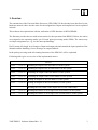
N O T E
The information in this document has been carefully checked and is believed to be entirely reliable.
esd makes no warranty of any kind with regard to the material in this document, and assumes no
responsibility for any errors that may appear in this document. In particular descriptions and
technical data specified in this document may not be constituted to be guaranteed product features
in any legal sense.
esd reserves the right to make changes without notice to this, or any of its products, to improve
reliability, performance or design.
All rights to this documentation are reserved by esd. Distribution to third parties, and reproduction
of this document in any form, whole or in part, are subject to esd's written approval.
© 2016 esd electronic system design gmbh, Hannover
esd electronic system design gmbh
Vahrenwalder Str. 207
30165 Hannover
Germany
Phone: +49-511-372 98-0
Fax: +49-511-372 98-68
E-Mail: [email protected]
Internet: www.esd.eu
This manual contains important information and instructions on safe and efficient
handling of the VME-DPIO32/63140. Carefully read this manual before commencing any
work and follow the instructions.
The manual is a product component, please retain it for future use.
Trademark Notices
All trademarks, product names, company names or company logos used in this manual are reserved by their
respective owners.
Page 2 of 38 Hardware Manual • Doc. No.: V.1607.21 / Rev. 2.2 VME-DPIO32/63140

Document file: I:\Texte\Doku\MANUALS\VME\DPIO32\Englisch\VME-DPIO32_Hardware_2.2.odt
Date of print: 2016-03-11
Document type
number: DOC0800
Hardware version: DPI32-5, with esd order No.: V.1607.04
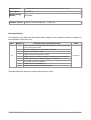
Document History
The changes in the document listed below affect changes in the hardware as well as changes in
the description of the facts, only.
Rev. Chapter Changes versus previous version Date
2.2
-Safety Instructions and Information and Classification of Warning messages
inserted, Manual restructured
2016-03-11
1. Block circuit diagram new, text according to data sheet
2. Chapter “Technical Data” revised
3. Chapter “Hardware Configuration” revised
4. Chapter “Interrupt Processing”, description of HD63140 and figure changed
5. Chapter “Digital Inputs and Outputs” description of HD63140
6. New Chapter “Hardware Installation”
7. Chapter “Connector Pin Assigments”
8. Chapter “Order Information” moved and revised
Technical details are subject to change without further notice.
VME-DPIO32/63140 Hardware Manual • Doc. No.: V.1607.21 / Rev. 2.2 Page 3 of 38

Classification of Warning Messages and Safety Instructions
This manual contains noticeable descriptions, warning messages and safety instructions, which
you must follow to avoid personal injuries or death and property damage.
This is the safety alert symbol.
It is used to alert you to potential personal injury hazards. Obey all safety messages
and instructions that follow this symbol to avoid possible injury or death.
DANGER, WARNING, CAUTION
Depending on the hazard level the signal words DANGER, WARNING or CAUTION are used to
highlight safety instructions and warning messages. These messages may also include a warning
relating to property damage.
DANGER
Danger statements indicate a hazardous situation which, if not avoided, will result in
death or serious injury.
WARNING
Warning statements indicate a hazardous situation that, if not avoided, could result in
death or serious injury.
CAUTION
Caution statements indicate a hazardous situation that, if not avoided, could result in
minor or moderate injury.
NOTICE
Notice statements are used to notify people on hazards that could result in things other than
personal injury, like property damage.
NOTICE
This NOTICE statement indicates that the device contains components sensitive to
electrostatic discharge.
NOTICE
This NOTICE statement contains the general mandatory sign and gives information that
must be heeded and complied with for a safe use.
INFORMATION
INFORMATION
Notes to point out something important or useful.
Page 4 of 38 Hardware Manual • Doc. No.: V.1607.21 / Rev. 2.2 VME-DPIO32/63140

Safety Instructions
● When working with the VME-DPIO32/63140 follow the instructions below and read the manual
carefully to protect yourself from injury and the VME-DPIO32/63140 from damage.
● The device is a built-in component. It is essential to ensure that the device is mounted in a way
that cannot lead to endangering or injury of persons or damage to objects.
● Do not use damaged or defective cables to connect the VME-DPIO32/63140.
● In case of damages to the device, which might affect safety, appropriate and immediate
measures must be taken, that exclude an endangerment of persons and domestic animals and
property.
● Current circuits which are connected to the device have to be sufficiently protected against
hazardous voltage (SELV according to EN 60950-1).
● The VME-DPIO32/63140 may only be driven by power supply current circuits, that are contact
protected.
A power supply, that provides a safety extra-low voltage (SELV) according to EN 60950-1,
complies with this conditions.
● The device has to be securely installed in the control cabinet before commissioning.
● Protect the VME-DPIO32/63140 from dust, moisture and steam.
● Protect the VME-DPIO32/63140 from shocks and vibrations.
● The VME-DPIO32/63140 may become warm during normal use. Always allow adequate
ventilation around the VME-DPIO32/63140 and use care when handling.
● Do not operate the VME-DPIO32/63140 adjacent to heat sources and do not expose it to
unnecessary thermal radiation. Ensure an ambient temperature as specified in the technical
data.
DANGER
Hazardous Voltage - Risk of electric shock due to unintentional contact with
uninsulated live parts with high voltages inside of the system into which the VME-
DPIO32/63140 is to be integrated.
→ Disconnect all hazardous voltages (mains voltage) before opening the system.
→ Ensure the absence of voltage before starting any electrical work
NOTICE
Electrostatic discharges may cause damage to electronic components.
To avoid this, perform the steps described on page 30 before you touch the VME-
DPIO32/63140, in order to discharge the static electricity from your body.
Qualified Personal
This documentation is directed exclusively towards personal qualified in control and automation
engineering. The installation and commissioning of the product may only be carried out by qualified
personal, which is authorized to put devices, systems and electric circuits into operation according to
the applicable national standards of safety engineering.
Conformity
The VME-DPIO32/63140 is a sub-assembly intended for incorporation into an apparatus by a
manufacturer and NOT by the end user. The manufacturer of the final system must decide, whether
additional EMC or EMI protection requirements are necessary.
Intended Use
The intended use of the VME-DPIO32/63140 is the operation as VME board with digital I/Os.
The guarantee given by esd does not cover damages which result from improper use, usage not in
accordance with regulations or disregard of safety instructions and warnings.
VME-DPIO32/63140 Hardware Manual • Doc. No.: V.1607.21 / Rev. 2.2 Page 5 of 38

● The VME-DPIO32/63140 is intended for installation in VMEbus systems only.
● The operation of the VME-DPIO32/63140 in hazardous areas, or areas exposed to potentially
explosive materials is not permitted.
● The operation of the VME-DPIO32/63140 for medical purposes is prohibited.
Service Note
The VME-DPIO32/63140 does not contain any parts that require maintenance by the user. The VME-
DPIO32/63140 does not require any manual configuration of the hardware. Unauthorized intervention in
the device voids warranty claims.
Disposal
Devices which have become defective in the long run have to be disposed in an appropriate way or
have to be returned to the manufacturer for proper disposal. Please, make a contribution to
environmental protection.
Page 6 of 38 Hardware Manual • Doc. No.: V.1607.21 / Rev. 2.2 VME-DPIO32/63140

Table of contents
Safety Instructions...........................................................................................................................5
1. Overview......................................................................................................................................8
2. Technical Data............................................................................................................................10
2.1 General Technical Data........................................................................................................10
2.2 VME specification.................................................................................................................11
2.3 Digital Outputs......................................................................................................................11
2.4 Digital Inputs........................................................................................................................12
2.5 Software Support................................................................................................................12
3. Hardware Configuration..............................................................................................................13
3.1 Front Panel View with LEDs.................................................................................................13
3.2 Address Covering of VME-DPIO32/63140...........................................................................14
3.3 Jumper Configuration...........................................................................................................15
3.3.1 Default Setting.............................................................................................................16
3.3.2 The Address-Modifier AM Jumper J3...........................................................................17
3.3.3 Basic Access Decoding via the Jumpers J1 and J2.....................................................21
4. Interrupt Processing...................................................................................................................22
5. Digital Inputs and Outputs..........................................................................................................24
5.1 Controller Assignment to Inputs and Outputs.......................................................................24
5.2 Pulse Processor HD63140 Structure...................................................................................26
5.3 Input and Output Circuit of VME-DPIO32/63140..................................................................27
5.3.1 General.......................................................................................................................27
5.3.2 Front Panel LEDs and Test Sockets............................................................................28
5.3.3 Input and Output Circuit Diagram................................................................................29
6. Hardware Installation..................................................................................................................30
7. Connector Pin Assigments.........................................................................................................31
7.1 VMEbus P1..........................................................................................................................31
7.2 I/O Connector P2.................................................................................................................32
7.3 Terminal Block I/O Connector P2 Phoenix FLKM64 or FLKMS64........................................33
7.4 Wiring Diagram....................................................................................................................34
8. Order Information.......................................................................................................................38
VME-DPIO32/63140 Hardware Manual • Doc. No.: V.1607.21 / Rev. 2.2 Page 7 of 38

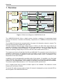
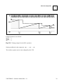
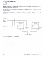
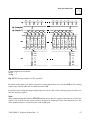
Overview
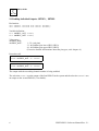
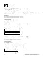
1. Overview
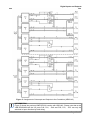
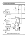
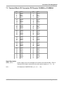
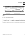
Figure 1: Block circuit diagram of VME-DPIO32/63140
The VME-DPIO32/63140 offers a digital process interface containing 32 optoisolated digital
process I/O channels. It includes all necessary components on a VMEbus 6U board and needs
one slot.
The 32 digital I/O channels are programmable in 8 groups of 4 channels as inputs or outputs. The
8 groups are electrically isolated from each other.
The input channels accept an input voltage range of 5 VDC to 30 VDC. Each input channel can
generate an interrupt on the VMEbus and that is programmable to rising or to falling edge. The
inputs are overvoltage protected between -3 VDC and +35 VDC. The digital output channels
accept an operating voltage range of 6 VDC to 28 VDC with a rated current of 0.3 A.
The outputs are driven by Quad High Side Drivers LMD18400. The protection circuit of the driver is
activated by short-circuit, over temperature and overvoltage. An error signal will be generated by
the drivers on the following conditions: no load, short circuit to GND, to VCC, overvoltage or over
temperature of the driver module.
In addition to the bit programmable operating mode of the outputs, it is possible to use the single
output channels via the pulse processor components HD63140 for pulse-width modulation (PWM).
A total of 2 x 24 programmable 16 bit registers for switching period and resolution are available.
The minimum pulse width amounts to 10 :s. The outputs can be synchronized.
Up to 4 digital inputs may be used as counter inputs at the CIO8536. The maximum counter
frequency for the inputs is 3 MHz.
The actual I/O status and error status of each I/O channel is displayed by a two coloured LED on
the front panel of the VME-DPIO32/63140.
Page 8 of 38 Hardware Manual • Doc. No.: V.1607.21 / Rev. 2.2 VME-DPIO32/63140
P1 VMEbus
LMD18400
Error
4 x Input
4 x Output
LMD18400
Error
4 x Input
4 x Output
4x
4x
VCC
VCC
VME Address
and
AM Decoder
Logic
VME
Interrupt
Control Logic
VME
Data Bus
Driver
Address, Data and Control Bus
CIO Z8536
16 Inputs +
Error Input
HD63140
16 Outputs
P2 8 Groups of Each 4 Channels
Electrical
Isolation
CIO Z8536
16 Inputs +
Error Input
HD63140
16 Outputs
Error
Error

Overview
Additionally, there are test sockets for each channel located on the front panel for stimulation of the
input channels or for disable of the output driver error signal.
The 64-pin adapter blocks VME-P2-ADAPT1 or VME-P2-ADAPT1 are connected via ribbon cable
to the P2 connector of the VME-DPIO32/63140. They offer wiring with screw or clamp terminals for
all P2 I/O signals.
To feed power supply for the 8 output groups separately (4 outputs are combined to one group) the
power adapter VMEDPIO32-P2VCC is used.
If a separate wiring of the output groups is not necessary the adapter VME-DPIO32-P2VCC-3X
feeds power to 3 VME-DPIO32/63140 installed in 3 VMEbus slots side-by-side is an economic
solution.
VME-DPIO32/63140 Hardware Manual • Doc. No.: V.1607.21 / Rev. 2.2 Page 9 of 38

Technical Data
2. Technical Data
2.1 General Technical Data
Digital power
supply voltage
VMEbus P1: 5V ± 5%
(typical values at 20 °C):
all outputs OFF:
all outputs ON:
16 outputs ON, 16 OFF:
all outputs OFF,
all inputs ON:
1.7 A
2.3 A
1.7 A
2.3 A
Electrical
isolation of inputs
and outputs
Pollution degree: Pollution degree: 2 (acc. to DIN EN 61131-2)
Over voltage category: II (acc. to DIN EN 61131-2)
Electrical isolation: functional isolation between I/O circuits and VMEbus,
dimensioning of air and creepage distances:
max. isolation working voltage Ue = 600 V AC/DC
(acc. to. DIN EN 61131-2, pollution degree 2,
over voltage category II)
max. isolation voltage of optocouplers
Urms = 2500 Vrms for 1 minute
Connector types P1-DIN 41612-C96
P2-DIN 41612-C64
Temperature
range 0...70 °C ambient temperature
Humidity max. 90%, non-condensing
Board size 160 mm x 233 mm
VME dimensions 6 U height / 1 slot width
Weight 470 g
Table 1: General data of the module
Page 10 of 38 Hardware Manual • Doc. No.: V.1607.21 / Rev. 2.2 VME-DPIO32/63140

Technical Data
2.2 VME specification
VME interface IEEE 1014 / D
Data transfer mode SADO24 - slave with A24/D16 access
SD16 - slave with A16/D16 access
Address modifier (AM) full evaluation of AM0 to AM5,
additionally 'AM2 don't care'
circuit possible
Basic address selectable by jumpers over the whole
address range of 16 Mbytes,
the board covers 4 kbytes
Interrupts I1 to I7 interrupter, level
programmable via HD63140
Table 2: VME interface
2.3 Digital Outputs
Quantity
32 (less inputs)
P-switching: Out = 24 V --> ’1’
Out = 0 V --> ’0’
Supply voltage Uvccmin = 6 V (DC)
Uvccmax = 28 V (DC)
Uvccrated = 24 V (DC)
Load capacity
(at 50°C)
rated current/channel (24 V): Ir = 0.3 A,
max. current/channel: limited by overtemperature protection
(see data sheet of LMD18400)
max. current/board: 16 A
signal level of outputs at rated current: ≥ Uvcc-2 V
Protective circuits short-circuit protection and overtemperature protection: electronically
with switch-off of output group,
overvoltage protection (triggering from Uvcc > 32 V..35 V)
Switching
performance
(at 20°)
values for Uvccrated and Ir: min. pulse time T ≥ 10 μs,
min. clock period TON ≥ 10 μs, TOFF ≥ 10 μs
(With this switching times the signal edges are bad. Additionally the times
may become longer due to circuit tolerance and ambient temperature.)
Electrical isolation
from VMEbus
potential
see description of electrical isolation in chapter “General Technical Data”,
page 10
Table 3: Data of the digital outputs
VME-DPIO32/63140 Hardware Manual • Doc. No.: V.1607.21 / Rev. 2.2 Page 11 of 38

Technical Data
2.4 Digital Inputs
Quantity 32 (less outputs)
Evaluation all inputs have interrupt capability max. 16 inputs at P2 configurable as
counter inputs, all 16 inputs connected to HD63140 and additionally
4 inputs in parallel to CIO Z8536 (higher resolution)
Input voltage
permissible input voltage range: -3 V ≤ Uin ≤ 30 V
Attention: If output driver LMD18400 is supplied by Uvccout, Uin may not
exceed Uin ≤ Uvccout - 2V !
(because of parallel connection to outputs)
threshold input = ’0’: Uout ≤ 2.0V
threshold input = ’1’: Uin ≥ 3.0V
Input current
Since the inputs and outputs are connected in parallel on the board, the
input current depends on the fact, whether the supply voltage is connected
to the output driver LMD18400:
input current/channel at Uvcc = 24 V (typical values at 20 °C):
input = ’1’: (5 V) Iin = 7.7 mA
(12 V) Iin = 9.9 mA
(22 V) Iin = 10.0 mA
input current/channel at Uvcc not supplied (typical values at 20 °C):
input = ’1’: (5 V) Iin = 8.0 mA
(12 V) Iin = 14.0 mA
(24 V) Iin = 30.0 mA
(30 V) Iin = 40.0 mA
Input frequency
input circuit (max.): 1 MHz (1:1)
counter frequency of controller HD63140 (depends on the complexity of
the functions):
just one function: thigh > 0.5 μs, tlow > 0.5 μs
fmax < 1 MHz (duty cycle 1:1)
16 functions: thigh > 5.0 μs, tlow > 5.0 μs
fmax < 100 kHz (duty cycle 1:1)
counter frequency of controller CIO 8536 max. 3 MHz
protective circuit
overvoltage protection by Transsil diode voltage-proof up to...
statically: Umax = 36 V
dynamically: Umax = 95 V (duty cycle 1/100, ton = 10 μs)
Umax = 225 V (duty cycle 1/1000, ton = 10 μs)
Electrical isolation
from VMEbus
potential
see description of electrical isolation in chapter “General Technical Data”,
page 10
Table 4: Data of the digital inputs
2.5 Software Support
Driver packages for VME-DPIO32/63140 are available e.g. for operating systems VxWorks and
OS9.
Page 12 of 38 Hardware Manual • Doc. No.: V.1607.21 / Rev. 2.2 VME-DPIO32/63140


Hardware Configuration
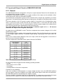
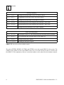
3.2 Address Covering of VME-DPIO32/63140
Address range D15-D8 D7-D0
nn ss FE
nn ss F8 CIO2
(Z8536) CIO1
(Z8536)
nn ss F6
nn ss F0 RAM of
HD2 (HD63140) RAM of
HD1 (HD63140)
nn ss DE
nn ss 00 HD2
(HD63140) HD1
(HD63140)
Table 5: Address Covering of VME-DPIO32/63140
nn ss .... basic address of DPIO32 for ’standard address accesses’
via VMEbus (A08 - A23 = CARD-ADDRESS)
ss ....... basic address of DPIO32 for ’short address accesses’
via VMEbus (A08 - A15 = CARD-ADDRESS)
Page 14 of 38 Hardware Manual • Doc. No.: V.1607.21 / Rev. 2.2 VME-DPIO32/63140

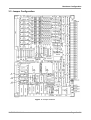
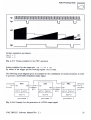
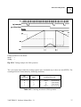
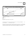
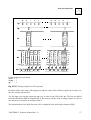
Hardware Configuration
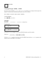
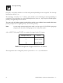
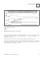
3.3 Jumper Configuration
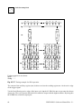
Figure 3: Jumper Position
VME-DPIO32/63140 Hardware Manual • Doc. No.: V.1607.21 / Rev. 2.2 Page 15 of 38

Hardware Configuration
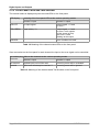
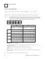
3.3.1 Default Setting
The particular factory-settings (of the jumpers see following table) are marked in the table.
The jumpers configuration can be obtained from the insertion diagram. An inserted jumper
corresponds to ’0’ (low) level of a signal.
In the following the jumpers are displayed in a position, as seen by the user, if he has the board
lying in front of himself with the VMEbus connectors to the rear end.
Default jumper setting of jumpers J1 to J4:
Jumper Function Setting
J1 basic address
A08-A15 basic address of VME-DPIO32/63140 set
to $xxE14000
J2 basic address
A16-A23
J3 address modifier AM2 don’t care, i.e. access in the supervisory
mode or user mode VME access A24/D16
Table 6: Default Jumper Setting
Page 16 of 38 Hardware Manual • Doc. No.: V.1607.21 / Rev. 2.2 VME-DPIO32/63140

Hardware Configuration
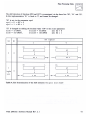
3.3.2 The Address-Modifier AM Jumper J3
The VME-DPIO32/63140 can be operated with access modes A24/D16 (standard) or A16/D16
(short).
At the default setting of jumpers displayed below A24/D16 accesses to the board are enabled. AM2
will be ignored, so user mode as well as supervisory mode can be used for addressing.
Default setting: Standard supervisory and non-privileged data access (A24-Mode)
The jumpers AM0, AM1 and AM4 are evaluated ’separately’. The jumpers AM2 and AM2E form a
unit and are always evaluated together.
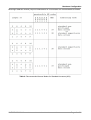
The jumpers AM0, AM1 and AM4 are evaluated as follows:
jumper/
pins
signal decoding
not inserted inserted
AM0
1-2
1 0
AM1
2-3
AM4
4-5
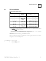
Table 7: Evaluation of Jumpers AM0, AM1 and AM4
VME-DPIO32/63140 Hardware Manual • Doc. No.: V.1607.21 / Rev. 2.2 Page 17 of 38

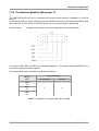
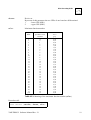
Hardware Configuration
Permissible Positions of Jumpers AM2 and AM2E are as follows:
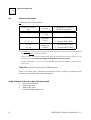
Table 8: Permissible positions of jumpers AM2 and AM2E
Page 18 of 38 Hardware Manual • Doc. No.: V.1607.21 / Rev. 2.2 VME-DPIO32/63140

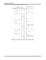
Hardware Configuration
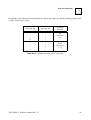
Meaningful address modifier jumpers combinations for 24 accesses are recommended as follows:
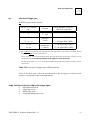
Table 9: Recommended Access Modes for Standard Accesses (A24)
VME-DPIO32/63140 Hardware Manual • Doc. No.: V.1607.21 / Rev. 2.2 Page 19 of 38

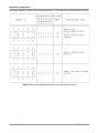
Hardware Configuration
Meaningful address modifier jumpers combinations for 16 accesses are recommended as follows:
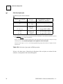
Table 10: Recommended Access Modes for Short Accesses (A16)
Page 20 of 38 Hardware Manual • Doc. No.: V.1607.21 / Rev. 2.2 VME-DPIO32/63140
Page is loading ...
Page is loading ...
Page is loading ...
Page is loading ...
Page is loading ...
Page is loading ...
Page is loading ...
Page is loading ...
Page is loading ...
Page is loading ...
Page is loading ...
Page is loading ...
Page is loading ...
Page is loading ...
Page is loading ...
Page is loading ...
Page is loading ...
Page is loading ...
Page is loading ...
Page is loading ...
Page is loading ...
Page is loading ...
Page is loading ...
Page is loading ...
Page is loading ...
Page is loading ...
Page is loading ...
Page is loading ...
Page is loading ...
Page is loading ...
Page is loading ...
Page is loading ...
Page is loading ...
Page is loading ...
Page is loading ...
Page is loading ...
Page is loading ...
Page is loading ...
Page is loading ...
Page is loading ...
Page is loading ...
Page is loading ...
Page is loading ...
Page is loading ...
Page is loading ...
Page is loading ...
Page is loading ...
Page is loading ...
Page is loading ...
Page is loading ...
Page is loading ...
Page is loading ...
Page is loading ...
Page is loading ...
Page is loading ...
Page is loading ...
Page is loading ...
Page is loading ...
Page is loading ...
Page is loading ...
Page is loading ...
Page is loading ...
Page is loading ...
Page is loading ...
Page is loading ...
Page is loading ...
Page is loading ...
Page is loading ...
Page is loading ...
Page is loading ...
Page is loading ...
Page is loading ...
Page is loading ...
Page is loading ...
Page is loading ...
Page is loading ...
Page is loading ...
Page is loading ...
Page is loading ...
Page is loading ...
Page is loading ...
Page is loading ...
Page is loading ...
Page is loading ...
Page is loading ...
Page is loading ...
-
 1
1
-
 2
2
-
 3
3
-
 4
4
-
 5
5
-
 6
6
-
 7
7
-
 8
8
-
 9
9
-
 10
10
-
 11
11
-
 12
12
-
 13
13
-
 14
14
-
 15
15
-
 16
16
-
 17
17
-
 18
18
-
 19
19
-
 20
20
-
 21
21
-
 22
22
-
 23
23
-
 24
24
-
 25
25
-
 26
26
-
 27
27
-
 28
28
-
 29
29
-
 30
30
-
 31
31
-
 32
32
-
 33
33
-
 34
34
-
 35
35
-
 36
36
-
 37
37
-
 38
38
-
 39
39
-
 40
40
-
 41
41
-
 42
42
-
 43
43
-
 44
44
-
 45
45
-
 46
46
-
 47
47
-
 48
48
-
 49
49
-
 50
50
-
 51
51
-
 52
52
-
 53
53
-
 54
54
-
 55
55
-
 56
56
-
 57
57
-
 58
58
-
 59
59
-
 60
60
-
 61
61
-
 62
62
-
 63
63
-
 64
64
-
 65
65
-
 66
66
-
 67
67
-
 68
68
-
 69
69
-
 70
70
-
 71
71
-
 72
72
-
 73
73
-
 74
74
-
 75
75
-
 76
76
-
 77
77
-
 78
78
-
 79
79
-
 80
80
-
 81
81
-
 82
82
-
 83
83
-
 84
84
-
 85
85
-
 86
86
-
 87
87
-
 88
88
-
 89
89
-
 90
90
-
 91
91
-
 92
92
-
 93
93
-
 94
94
-
 95
95
-
 96
96
-
 97
97
-
 98
98
-
 99
99
-
 100
100
-
 101
101
-
 102
102
-
 103
103
-
 104
104
-
 105
105
-
 106
106


Ask a question and I''ll find the answer in the document
Finding information in a document is now easier with AI
Related papers
Other documents
-
Motorola MVME2700-3361 Datasheet
-
-
Motorola MVME2600 Series Datasheet
-
-
-
-
-
-
-
Eurolux O30R Owner's manual