Vishay IRF830AS Owner's manual

Type
Owner's manual

Vishay IRF830AS is a N-Channel MOSFET that offers low gate charge, leading to simple drive requirements. It features improved gate, avalanche, and dynamic dV/dt ruggedness and can handle high power applications with ease. The device is fully characterized for capacitance, avalanche voltage, and current, making it suitable for various high-performance applications.

Vishay IRF830AS is a N-Channel MOSFET that offers low gate charge, leading to simple drive requirements. It features improved gate, avalanche, and dynamic dV/dt ruggedness and can handle high power applications with ease. The device is fully characterized for capacitance, avalanche voltage, and current, making it suitable for various high-performance applications.

IRF830AS, IRF830AL, SiHF830AS, SiHF830AL
www.vishay.com Vishay Siliconix
S21-0901-Rev. D, 30-Aug-2021 1Document Number: 91062
For technical questions, contact: hvm@vishay.com
THIS DOCUMENT IS SUBJECT TO CHANGE WITHOUT NOTICE. THE PRODUCTS DESCRIBED HEREIN AND THIS DOCUMENT
ARE SUBJECT TO SPECIFIC DISCLAIMERS, SET FORTH AT www.vishay.com/doc?91000
Power MOSFET
FEATURES
Low gate charge Qg results in simple drive
requirement
Improved gate, avalanche and dynamic dV/dt
ruggedness
Fully characterized capacitance and avalanche
voltage and current
Effective Coss specified
Material categorization: for definitions of compliance
please see www.vishay.com/doc?99912
Note
*
This datasheet provides information about parts that are
RoHS-compliant and / or parts that are non RoHS-compliant. For
example, parts with lead (Pb) terminations are not RoHS-compliant.
Please see the information / tables in this datasheet for details
APPLICATIONS
Switch mode power supply (SMPS)
Uninterruptible power supply
High speed power switching
TYPICAL SMPS TOPOLOGIES
Two transistor forward
Half bridge and full bridge
Note
a. See device orientation
Notes
a. Repetitive rating; pulse width limited by maximum junction temperature (see fig. 11)
b. Starting TJ = 25 °C, L = 18 mH, Rg = 25 Ω, IAS = 5.0 A (see fig. 12)
c. ISD 5.0 A, dI/dt 370 A/μs, VDD VDS, TJ 150 °C
d. 1.6 mm from case
e. Uses SiHF830A data and test conditions
PRODUCT SUMMARY
VDS (V) 500
RDS(on) max. (Ω)V
GS = 10 V 1.40
Qg max. (nC) 24
Qgs (nC) 6.3
Qgd (nC) 11
Configuration Single
N-Channel MOSFET
G
D
S
D
2
PAK (TO-2
GD
S
I
2
PAK (TO-262)
GDS
Available
Available
ORDERING INFORMATION
Package D2PAK (TO-263) D2PAK (TO-263) I2PAK (TO-262)
Lead (Pb)-free and Halogen-free SiHF830AS-GE3 SiHF830ASTRL-GE3 a SiHF830AL-GE3 a
Lead (Pb)-free IRF830ASPbF IRF830ASTRLPbF a IRF830ALPbF
ABSOLUTE MAXIMUM RATINGS (TC = 25 °C, unless otherwise noted)
PARAMETER SYMBOL LIMIT UNIT
Drain-Source Voltage VDS 500 V
Gate-Source Voltage VGS ± 30
Continuous Drain Current VGS at 10 V TC = 25 °C ID
5.0
ATC = 100 °C 3.2
Pulsed Drain Current a, e IDM 20
Linear Derating Factor 0.59 W/°C
Single Pulse Avalanche Energy b, e EAS 230 mJ
Avalanche Currenta IAR 5.0 A
Repetiitive Avalanche Energy a EAR 7.4 mJ
Maximum Power Dissipation TA = 25 °C PD
3.1 W
TC = 25 °C 74
Peak Diode Recovery dV/dtc, edV/dt 5.3 V/ns
Operating Junction and Storage Temperature Range TJ, Tstg -55 to +150 °C
Soldering Recommendations (Peak temperature) dfor 10 s 300
Downloaded from Arrow.com.
IRF830AS, IRF830AL, SiHF830AS, SiHF830AL
www.vishay.com Vishay Siliconix
S21-0901-Rev. D, 30-Aug-2021 2Document Number: 91062
For technical questions, contact: hvm@vishay.com
THIS DOCUMENT IS SUBJECT TO CHANGE WITHOUT NOTICE. THE PRODUCTS DESCRIBED HEREIN AND THIS DOCUMENT
ARE SUBJECT TO SPECIFIC DISCLAIMERS, SET FORTH AT www.vishay.com/doc?91000
Note
a. When mounted on 1" square PCB (FR-4 or G-10 material)
Notes
a. Repetitive rating; pulse width limited by maximum junction temperature (see fig. 11)
b. Pulse width 300 μs; duty cycle 2 %
c. Coss eff. is a fixed capacitance that gives the same charging time as Coss while VDS is rising from 0 to 80 % VDS
d. Uses SiHF830A data and test conditions
THERMAL RESISTANCE RATINGS
PARAMETER SYMBOL TYP. MAX. UNIT
Maximum Junction-to-Ambient
(PCB mounted, steady-state) aRthJA -40
°C/W
Maximum Junction-to-Case (Drain) RthJC -1.7
SPECIFICATIONS (TJ = 25 °C, unless otherwise noted)
PARAMETER SYMBOL TEST CONDITIONS MIN. TYP. MAX. UNIT
Static
Drain-Source Breakdown Voltage VDS VGS = 0, ID = 250 μA 500 - - V
VDS Temperature Coefficient ΔVDS/TJ Reference to 25 °C, ID = 1 mA d -0.60-V/°C
Gate-Source Threshold Voltage VGS(th) VDS = VGS, ID = 250 μA 2.0 - 4.5 V
Gate-Source Leakage IGSS V
GS = ± 30 V - - ± 100 nA
Zero Gate Voltage Drain Current IDSS
VDS = 500 V, VGS = 0 V - - 25 μA
VDS = 400 V, VGS = 0 V, TJ = 125 °C - - 250
Drain-Source On-State Resistance RDS(on) V
GS = 10 V ID = 3.0 A b --1.4Ω
Forward Transconductance gfs VDS = 50 V, ID = 3.0 A d2.8 - - S
Dynamic
Input Capacitance Ciss VGS = 0 V,
VDS = 25 V,
f = 1.0 MHz, see fig. 5 d
- 620 -
pFOutput Capacitance Coss -93-
Reverse Transfer Capacitance Crss -4.3-
Output Capacitance Coss VGS = 0 V
VDS = 1.0 V, f = 1.0 MHz - 886 -
VDS = 400 V, f = 1.0 MHz - 27 -
Effective Output Capacitance Coss eff. VDS = 0 V to 400 V c, d -39-
Total Gate Charge Qg
VGS = 10 V ID = 5.0 A, VDS = 400 V,
see fig. 6 and 13 b, d
--24
nC Gate-Source Charge Qgs --6.3
Gate-Drain Charge Qgd --11
Turn-On Delay Time td(on)
VDD = 250 V, ID = 5.0 A,
Rg = 14 Ω, RD = 49 Ω, see fig. 10 b, d
-10-
ns
Rise Time tr -21-
Turn-Off Delay Time td(off) -21-
Fall Time tf -15-
Gate Input Resistance Rgf = 1 MHz, open drain 1.7 - 10.7 Ω
Drain-Source Body Diode Characteristics
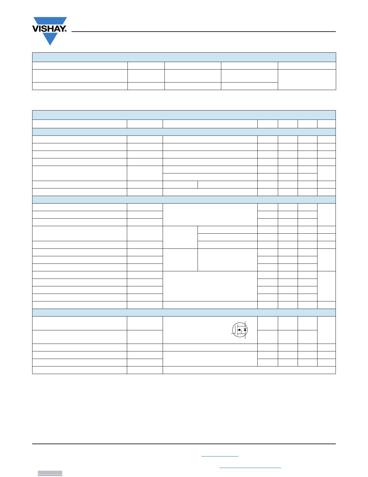
Continuous Source-Drain Diode Current ISMOSFET symbol
showing the
integral reverse
p - n junction diode
--5.0
A
Pulsed Diode Forward Current a ISM --20
Body Diode Voltage VSD TJ = 25 °C, IS = 5.0 A, VGS = 0 V b --1.5V
Body Diode Reverse Recovery Time trr TJ = 25 °C, IF = 5.0 A, dI/dt = 100 A/μs b, d - 430 650 ns
Body Diode Reverse Recovery Charge Qrr -2.03.0μC
Forward Turn-On Time ton Intrinsic turn-on time is negligible (turn-on is dominated by LS and LD)
S
D
G
Downloaded from Arrow.com.Downloaded from Arrow.com.
IRF830AS, IRF830AL, SiHF830AS, SiHF830AL
www.vishay.com Vishay Siliconix
S21-0901-Rev. D, 30-Aug-2021 3Document Number: 91062
For technical questions, contact: hvm@vishay.com
THIS DOCUMENT IS SUBJECT TO CHANGE WITHOUT NOTICE. THE PRODUCTS DESCRIBED HEREIN AND THIS DOCUMENT
ARE SUBJECT TO SPECIFIC DISCLAIMERS, SET FORTH AT www.vishay.com/doc?91000
TYPICAL CHARACTERISTICS (25 °C, unless otherwise noted)
Fig. 1 - Typical Output Characteristics
Fig. 2 - Typical Output Characteristics
Fig. 3 - Typical Transfer Characteristics
Fig. 4 - Normalized On-Resistance vs. Temperature
Fig. 5 - Typical Capacitance vs. Drain-to-Source Voltage
Fig. 6 - Typical Gate Charge vs. Gate-to-Source Voltage
91062_01
Bottom
To p
VGS
15 V
10 V
8.0 V
7.0 V
6.0 V
5.5 V
5.0 V
4.5 V
20 µs Pulse Width
TJ = 25 °C
4.5 V
VDS, Drain-to-Source Voltage (V)
ID, Drain-to-Source Current (A)
10
102
10
10-2
1
0.1
0.1 1 102
V
DS,
Drain-to-Source Voltage (V)
I
D
, Drain-to-Source Current (A)
Bottom
To p
VGS
15 V
10 V
8.0 V
7.0 V
6.0 V
5.5 V
5.0 V
4.5 V
20 µs Pulse Width
TJ = 150 °C
91062_02
4.5 V
102
10
1
0.1
10110
2
20 µs Pulse Width
VDS = 50 V
ID, Drain-to-Source Current (A)
VGS, Gate-to-Source Voltage (V)
5.0 6.0 7.0 8.04.0
91062_03
TJ = 25 °C
TJ = 150 °C
102
10
1
0.1
I
D
= 5.0 A
V
GS
= 10 V
0.0
0.5
1.0
1.5
2.0
2.5
T
J,
Junction Temperature (°C)
R
DS(on)
, Drain-to-Source On Resistance
(Normalized)
91062_04
- 60 - 40 - 20 0 20 40 60 80 100 120 140 160
10 102
C, Capacitance (pF)
VDS, Drain-to-Source Voltage (V)
Ciss
Crss
Coss
VGS = 0 V, f = 1 MHz
Ciss = Cgs + Cgd, Cds Shorted
Crss = Cgd
Coss = Cds + Cgd
91062_05
103
1
104
103
102
10
1
QG, Total Gate Charge (nC)
VGS, Gate-to-Source Voltage (V)
20
16
12
8
0
4
824
2016
12
V
DS
= 100 V
V
DS
= 250 V
For test circuit
see figure 13
V
DS
= 400 V
91062_06
I
D
= 5.0 A
40
Downloaded from Arrow.com.Downloaded from Arrow.com.Downloaded from Arrow.com.
IRF830AS, IRF830AL, SiHF830AS, SiHF830AL
www.vishay.com Vishay Siliconix
S21-0901-Rev. D, 30-Aug-2021 4Document Number: 91062
For technical questions, contact: hvm@vishay.com
THIS DOCUMENT IS SUBJECT TO CHANGE WITHOUT NOTICE. THE PRODUCTS DESCRIBED HEREIN AND THIS DOCUMENT
ARE SUBJECT TO SPECIFIC DISCLAIMERS, SET FORTH AT www.vishay.com/doc?91000
Fig. 7 - Typical Source-Drain Diode Forward Voltage
Fig. 8 - Maximum Safe Operating Area
Fig. 9 - Maximum Drain Current vs. Case Temperature
Fig. 10a - Switching Time Test Circuit
Fig. 10b - Switching Time Waveforms
Fig. 11 - Maximum Effective Transient Thermal Impedance, Junction-to-Case
102
10
V
SD
, Source-to-Drain Voltage (V)
I
SD
, Reverse Drain Current (A)
0.2 1.0
0.80.60.4
V
GS
= 0 V
91062_07
TJ = 25 °C
TJ = 150 °C
1
0.1
1.2
10 µs
100 µs
1 ms
10 ms
Operation in this area limited
by RDS(on)
VDS, Drain-to-Source Voltage (V)
ID, Drain Current (A)
TC = 25 °C
TJ = 150 °C
Single Pulse
102
0.1
1
10
10 102103104
91062_08
Pulse width 1 µs
Duty factor 0.1 %
RD
VGS
Rg
D.U.T.
10 V
+
-
VDS
VDD
VDS
90 %
10 %
VGS
td(on) trtd(off) tf
10
1
0.1
10-2
10-5 10-4 10-3 10-2 0.1 1
PDM
t1
t2
t1, Rectangular Pulse Duration (s)
Thermal Response (ZthJC)
Notes:
1. Duty Factor, D = t1/t2
2. Peak Tj = PDM x ZthJC + TC
Single Pulse
(Thermal Response)
D = 0.50
0.20
0.05
0.02
0.01
91062_11
0.10
Downloaded from Arrow.com.Downloaded from Arrow.com.Downloaded from Arrow.com.Downloaded from Arrow.com.
IRF830AS, IRF830AL, SiHF830AS, SiHF830AL
www.vishay.com Vishay Siliconix
S21-0901-Rev. D, 30-Aug-2021 5Document Number: 91062
For technical questions, contact: hvm@vishay.com
THIS DOCUMENT IS SUBJECT TO CHANGE WITHOUT NOTICE. THE PRODUCTS DESCRIBED HEREIN AND THIS DOCUMENT
ARE SUBJECT TO SPECIFIC DISCLAIMERS, SET FORTH AT www.vishay.com/doc?91000
Fig. 12a - Unclamped Inductive Test Circuit
Fig. 12b - Unclamped Inductive Waveforms
Fig. 12c - Maximum Avalanche Energy vs. Drain Current
Fig. 13a - Maximum Avalanche Energy vs. Drain Current
Fig. 12d - Basic Gate Charge Waveform
Fig. 13b - Gate Charge Test Circuit
A
Rg
IAS
0.01 Ω
tp
D.U.T.
L
VDS
+
-VDD
Driver
15 V
20 V
IAS
VDS
tp
QGS QGD
QG
V
G
Charge
VGS
785
770
775
780
0.0 5.04.03.02.01.0
I
AV
, Avalanche Current (A)
V
DSav
, Avalanche Voltage (V)
790
91062_12d
D.U.T.
3 mA
VGS
VDS
IGID
0.3 µF
0.2 µF
50 kΩ
12 V
Current regulator
Current sampling resistors
Same type as D.U.T.
+
-
Downloaded from Arrow.com.Downloaded from Arrow.com.Downloaded from Arrow.com.Downloaded from Arrow.com.Downloaded from Arrow.com.
IRF830AS, IRF830AL, SiHF830AS, SiHF830AL
www.vishay.com Vishay Siliconix
S21-0901-Rev. D, 30-Aug-2021 6Document Number: 91062
For technical questions, contact: hvm@vishay.com
THIS DOCUMENT IS SUBJECT TO CHANGE WITHOUT NOTICE. THE PRODUCTS DESCRIBED HEREIN AND THIS DOCUMENT
ARE SUBJECT TO SPECIFIC DISCLAIMERS, SET FORTH AT www.vishay.com/doc?91000
Fig. 14 - For N-Channel
Vishay Siliconix maintains worldwide manufacturing capability. Products may be manufactured at one of several qualified locations. Reliability data for Silicon
Technology and Package Reliability represent a composite of all qualified locations. For related documents such as package/tape drawings, part marking, and
reliability data, see www.vishay.com/ppg?91062.
P.W. Period
dI/dt
Diode recovery
dV/dt
Ripple 5 %
Body diode forward drop
Re-applied
voltage
Reverse
recovery
current
Body diode forward
current
VGS = 10 Va
ISD
Driver gate drive
D.U.T. lSD waveform
D.U.T. VDS waveform
Inductor current
D = P.W.
Period
+
-
+
+
+
-
-
-
Peak Diode Recovery dV/dt Test Circuit
VDD
dV/dt controlled by Rg
Driver same type as D.U.T.
ISD controlled by duty factor “D”
D.U.T. - device under test
D.U.T. Circuit layout considerations
Low stray inductance
Ground plane
Low leakage inductance
current transformer
Rg
Note
a. VGS = 5 V for logic level devices
VDD
Downloaded from Arrow.com.Downloaded from Arrow.com.Downloaded from Arrow.com.Downloaded from Arrow.com.Downloaded from Arrow.com.Downloaded from Arrow.com.
Document Number: 91364 www.vishay.com
Revision: 15-Sep-08 1
Package Information
Vishay Siliconix
TO-263AB (HIGH VOLTAGE)
Notes
1. Dimensioning and tolerancing per ASME Y14.5M-1994.
2. Dimensions are shown in millimeters (inches).
3. Dimension D and E do not include mold flash. Mold flash shall not exceed 0.127 mm (0.005") per side. These dimensions are measured at the
outmost extremes of the plastic body at datum A.
4. Thermal PAD contour optional within dimension E, L1, D1 and E1.
5. Dimension b1 and c1 apply to base metal only.
6. Datum A and B to be determined at datum plane H.
7. Outline conforms to JEDEC outline to TO-263AB.
5
4
13
L1
L2
D
BB
E
H
B
A
Detail A
A
A
c
c2
A
2 x e
2 x b2
2 x b
0.010 A B
MM ± 0.004 B
M
Base
metal
Plating b1, b3
(b, b2)
c1
(c)
Section B - B and C - C
Scale: none
Lead tip
4
34
(Datum A)
2CC
BB
5
5
View A - A
E1
D1
E
4
4
B
H
Seating plane
Gauge
plane
0° to 8°
Detail “A”
Rotated 90° CW
scale 8:1
L3 A1
L4
L
MILLIMETERS INCHES MILLIMETERS INCHES
DIM. MIN. MAX. MIN. MAX. DIM. MIN. MAX. MIN. MAX.
A 4.06 4.83 0.160 0.190 D1 6.86 - 0.270 -
A1 0.00 0.25 0.000 0.010 E 9.65 10.67 0.380 0.420
b 0.51 0.99 0.020 0.039 E1 6.22 - 0.245 -
b1 0.51 0.89 0.020 0.035 e 2.54 BSC 0.100 BSC
b2 1.14 1.78 0.045 0.070 H 14.61 15.88 0.575 0.625
b3 1.14 1.73 0.045 0.068 L 1.78 2.79 0.070 0.110
c 0.38 0.74 0.015 0.029 L1 - 1.65 - 0.066
c1 0.38 0.58 0.015 0.023 L2 - 1.78 - 0.070
c2 1.14 1.65 0.045 0.065 L3 0.25 BSC 0.010 BSC
D 8.38 9.65 0.330 0.380 L4 4.78 5.28 0.188 0.208
ECN: S-82110-Rev. A, 15-Sep-08
DWG: 5970
Downloaded from Arrow.com.Downloaded from Arrow.com.Downloaded from Arrow.com.Downloaded from Arrow.com.Downloaded from Arrow.com.Downloaded from Arrow.com.Downloaded from Arrow.com.
Document Number: 91367 www.vishay.com
Revision: 27-Oct-08 1
Package Information
Vishay Siliconix
I2PAK (TO-262) (HIGH VOLTAGE)
Notes
1. Dimensioning and tolerancing per ASME Y14.5M-1994.
2. Dimension D and E do not include mold flash. Mold flash shall not exceed 0.127 mm per side. These dimensions are measured at the outmost
extremes of the plastic body.
3. Thermal pad contour optional within dimension E, L1, D1, and E1.
4. Dimension b1 and c1 apply to base metal only.
A
E
B
A
A
A
c2
c
A1
Base
metal
Plating b1, b3
(b, b2)
c1
c
Section A - A
Section B - B and C - C
Scale: None
E1
E
Seating
plane
Lead tip
(Datum A)
L1
L2
BB
CC
L
D
2 x e
3 x b2
3 x b
0.010 A B
MM
D1
MILLIMETERS INCHES MILLIMETERS INCHES
DIM. MIN. MAX. MIN. MAX. DIM. MIN. MAX. MIN. MAX.
A 4.06 4.83 0.160 0.190 D 8.38 9.65 0.330 0.380
A1 2.03 3.02 0.080 0.119 D1 6.86 - 0.270 -
b 0.51 0.99 0.020 0.039 E 9.65 10.67 0.380 0.420
b1 0.51 0.89 0.020 0.035 E1 6.22 - 0.245 -
b2 1.14 1.78 0.045 0.070 e 2.54 BSC 0.100 BSC
b3 1.14 1.73 0.045 0.068 L 13.46 14.10 0.530 0.555
c 0.38 0.74 0.015 0.029 L1 - 1.65 - 0.065
c1 0.38 0.58 0.015 0.023 L2 3.56 3.71 0.140 0.146
c2 1.14 1.65 0.045 0.065
ECN: S-82442-Rev. A, 27-Oct-08
DWG: 5977
Downloaded from Arrow.com.Downloaded from Arrow.com.Downloaded from Arrow.com.Downloaded from Arrow.com.Downloaded from Arrow.com.Downloaded from Arrow.com.Downloaded from Arrow.com.Downloaded from Arrow.com.
AN826
Vishay Siliconix
Document Number: 73397
11-Apr-05
www.vishay.com
1
RECOMMENDED MINIMUM PADS FOR D2PAK: 3-Lead
0.635
(16.129)
Recommended Minimum Pads
Dimensions in Inches/(mm)
0.420
(10.668)
0.355
(9.017)
0.145
(3.683)
0.135
(3.429)
0.200
(5.080)
0.050
(1.257)
Return to Index
Downloaded from Arrow.com.Downloaded from Arrow.com.Downloaded from Arrow.com.Downloaded from Arrow.com.Downloaded from Arrow.com.Downloaded from Arrow.com.Downloaded from Arrow.com.Downloaded from Arrow.com.Downloaded from Arrow.com.
Legal Disclaimer Notice
www.vishay.com Vishay
Revision: 01-Jan-2023 1Document Number: 91000
Disclaimer
ALL PRODUCT, PRODUCT SPECIFICATIONS AND DATA ARE SUBJECT TO CHANGE WITHOUT NOTICE TO IMPROVE
RELIABILITY, FUNCTION OR DESIGN OR OTHERWISE.
Vishay Intertechnology, Inc., its affiliates, agents, and employees, and all persons acting on its or their behalf (collectively,
“Vishay”), disclaim any and all liability for any errors, inaccuracies or incompleteness contained in any datasheet or in any other
disclosure relating to any product.
Vishay makes no warranty, representation or guarantee regarding the suitability of the products for any particular purpose or
the continuing production of any product. To the maximum extent permitted by applicable law, Vishay disclaims (i) any and all
liability arising out of the application or use of any product, (ii) any and all liability, including without limitation special,
consequential or incidental damages, and (iii) any and all implied warranties, including warranties of fitness for particular
purpose, non-infringement and merchantability.
Statements regarding the suitability of products for certain types of applications are based on Vishay's knowledge of typical
requirements that are often placed on Vishay products in generic applications. Such statements are not binding statements
about the suitability of products for a particular application. It is the customer's responsibility to validate that a particular product
with the properties described in the product specification is suitable for use in a particular application. Parameters provided in
datasheets and / or specifications may vary in different applications and performance may vary over time. All operating
parameters, including typical parameters, must be validated for each customer application by the customer's technical experts.
Product specifications do not expand or otherwise modify Vishay's terms and conditions of purchase, including but not limited
to the warranty expressed therein.
Hyperlinks included in this datasheet may direct users to third-party websites. These links are provided as a convenience and
for informational purposes only. Inclusion of these hyperlinks does not constitute an endorsement or an approval by Vishay of
any of the products, services or opinions of the corporation, organization or individual associated with the third-party website.
Vishay disclaims any and all liability and bears no responsibility for the accuracy, legality or content of the third-party website
or for that of subsequent links.
Except as expressly indicated in writing, Vishay products are not designed for use in medical, life-saving, or life-sustaining
applications or for any other application in which the failure of the Vishay product could result in personal injury or death.
Customers using or selling Vishay products not expressly indicated for use in such applications do so at their own risk. Please
contact authorized Vishay personnel to obtain written terms and conditions regarding products designed for such applications.
No license, express or implied, by estoppel or otherwise, to any intellectual property rights is granted by this document or by
any conduct of Vishay. Product names and markings noted herein may be trademarks of their respective owners.
© 2023 VISHAY INTERTECHNOLOGY, INC. ALL RIGHTS RESERVED
Downloaded from Arrow.com.Downloaded from Arrow.com.Downloaded from Arrow.com.Downloaded from Arrow.com.Downloaded from Arrow.com.Downloaded from Arrow.com.Downloaded from Arrow.com.Downloaded from Arrow.com.Downloaded from Arrow.com.Downloaded from Arrow.com.
  • Page 1 1
  • Page 2 2
  • Page 3 3
  • Page 4 4
  • Page 5 5
  • Page 6 6
  • Page 7 7
  • Page 8 8
  • Page 9 9
  • Page 10 10

Vishay IRF830AS Owner's manual

Type
Owner's manual

Vishay IRF830AS is a N-Channel MOSFET that offers low gate charge, leading to simple drive requirements. It features improved gate, avalanche, and dynamic dV/dt ruggedness and can handle high power applications with ease. The device is fully characterized for capacitance, avalanche voltage, and current, making it suitable for various high-performance applications.

Ask a question and I''ll find the answer in the document

Finding information in a document is now easier with AI