
TLP848
2007-10-01
1
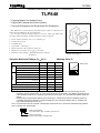
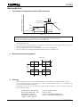
TOSHIBA Photointerrupter Infrared LED + Phototransistor
TLP848
○ Camera Module for Mobile Phone
○ Digital Still Camera and Video Camera
○ Personal Equipment and Small-sized OA Equipment
The TLP848 is a surface-mount photointerrupter which is composed of a
GaAs infrared LED and a Si phototransistor.
It is an ultra compact package. Moreover it has a wider gap width than
1mm gap width of industry-standard and has a high resolution.
• Ultra compact package : 2.8×1.9×2.5mm (typ.)
• Surface-mount type
• Lead(Pb)-Free
• Gap width : 1.2mm (typ.)
• High resolution : Slit width 0.3 mm (typ.)
• High current transfer ratio : I
C
/I
F
= 3% (min)
• Material of the package : PPS (Polyphenylene sulfide)
(UL94V-0)
Absolute Maximum Ratings
(Ta
=
25°C
) Marking (Note 2)
Characteristics Symbol Rating Unit
Forward current I
F
30 mA
Forward current derating (Ta>25°C) ΔI
F/
°C −0.33 mA/°C
LED
Reverse voltage V
R
5 V
Collector-emitter voltage V
CEO
15 V
Emitter-collector voltage V
ECO
5 V
Collector power dissipation P
C
75 mW
Collector power dissipation derating
(Ta>25℃)
ΔP
C/
°C −1 mW/°C
Detector
Collector current I
C
50 mA
Operating temperature range T
opr
−30 to 85 °C
Storage temperature range T
stg
−40 to 100 °C
Soldering temperature (Note 1) T
sol
250 °C
Note: Using continuously under heavy loads (e.g. the application of high temperature/current/voltage and the
significant change in temperature, etc.) may cause this product to decrease in the reliability significantly even
if the operating conditions (i.e. operating temperature/current/voltage, etc.) are within the absolute maximum
ratings.
Please design the appropriate reliability upon reviewing the Toshiba Semiconductor Reliability Handbook
(“Handling Precautions”/“Derating Concept and Methods”) and individual reliability data (i.e. reliability test
report and estimated failure rate, etc).
Note 1: The reflow time and the example of temperature profile are shown in the section entitled Mounting Method.
Note 2: Weekly code: (Three digits)
TOSHIBA 11-3B1
Weight: 0.017 g (typ.)
Weekly Code
Week of manufacture
(01 for first week of year, continues up to 52 or 53)
Year of manufacture
(One low-order digits of calendar year)

TLP848
2007-10-01
2
Optical and Electrical Characteristics
(Ta
=
25°C)
Characteristics Symbol Test conditions Min Typ. Max Unit
Forward voltage V
F
I
F
= 10 mA 1.10 1.23 1.40 V
Reverse current I
R
V
R
= 5 V ⎯ ⎯ 10 μA
LED
Peak emission wavelength λ
P
I
F
= 10 mA ⎯ 940 ⎯ nm
Dark current I
D
(I
CEO
) V
CE
= 12 V, I
F
= 0 ⎯ ⎯ 0.05 μA
Detector
Peak sensitivity wavelength λ
P
⎯ ⎯ 820 ⎯ nm
TLP848 3 ⎯ 24 %
Current transfer ratio I
C
/I
F
V
CE
= 2 V
I
F
= 5 mA
TLP848 (R) 4 ⎯ 20 %
Collector-emitter saturation
voltage
V
CE (sat)
I
F
= 10 mA, I
C
= 0.15 mA ⎯ 0.1 0.4 V
Rise time t
r
⎯ 15 50
Coupled
Fall time t
f
V
CC
= 5 V, I
C
= 1 mA
R
L
= 1k Ω (Note 3)
⎯ 15 50
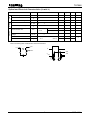
μs
Note 3: Switching time measurement circuit and waveform
V
CC
V
OUT
R
L
I
F
V
OUT
I
F
t
r
90%
10%
t
f
t
d
t
s

TLP848
2007-10-01
3
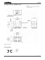
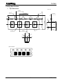
Package Dimensions: TOSHIBA 11-3B1
Weight: 0.017 g (typ.)
Pin Connection
Unit: mm
Tolerance : ±0.1mm unless otherwise specified
( ): Reference value
Gate position
Center of sensor
1: Cathode
2: Anode
3: Collector
4: Emitter
2
1
3
4

TLP848
2007-10-01
4
Handling and Mounting Precautions
• Care must be taken in relation to the environment in which the device is to be installed. Oil or chemicals
may cause the package to melt or crack.
• The device should be mounted on an unwarped surface.
• Do not apply stress to the resin at high temperature.
• The resin part is easily scratched, so avoid friction with hard materials.
• When installing the assembly board in equipment, ensure that this product does not come into contact with
other components.
• Conversion efficiency falls over time due to the current which flows in the infrared LED. When designing a
circuit, take into account this change in conversion efficiency over time. The ratio of fluctuation in
conversion efficiency to fluctuation in infrared LED optical output is 1:1.
Moisture-Proof Packing
• To avoid moisture absorption, the reel is packed in an aluminum bag that contains a desiccant with a
humidity indicator. Since the optical characteristics of the photointerrputer may be affected during soldering
by vaporization of the moisture which is absorbed in storable period, it should be stored under the following
conditions:
1. If the aluminum bag has been stored unopened
Temperature: 5 to 30°C
Relative humidity: 90% RH (max)
Time: 12 months
2. If the aluminum bag has been opened
Temperature: 5 to 30°C
Relative humidity: 70% RH (max)
Time: 168 h
3. Baking should be conducted within 72 h after the humidity indicator shows > 30% or the bag seal date
is over 12 months. The number of baking should be once. If the baking is conducted repeatedly, it may
affect the peel-back force and cause a problem for mounting.
Baking condition: 60 ± 5°C, 12 to 24 h
Storage period: 12 months from the seal date on the label
4. When the photointerrupter is baked, protect it from electrostatic discharge.
5. Do not toss or drop to avoid damaging the moisture-proof bag.
I
C
/I
F (t)
I
C
/I
F (0)
=
P
o (t)
P
o (0)

TLP848
2007-10-01
5
Mounting Methods
1. The example of temperature profile (reflow soldering)
• The first reflow process should be performed under the above temperature profile within 168 h
after opening the bag.
• If a second reflow process needs to be performed, it should be performed within 168 h of the first
reflow under the above temperature profile.
• Storage conditions before the second reflow process: 30°C, 70% RH (max)
• Do not perform wave soldering and manual soldering with a soldering iron.
2. Recommended soldering pattern
Unit: mm
3. Cleaning
When cleaning is required after soldering, Toshiba recommends the following cleaning solvents.
It is confirmed that these solvents have no effect on semiconductor devices in our dipping test
(under the recommended conditions).
In selecting the one for your actual usage, please perform sufficient review on washing condition,
using condition and etc.
ASAHI CLEAN AK-225AES : (made by ASAHI GLASS)
KAO CLEAN TROUGH 750H : (made by KAO)
PINE ALPHA ST-100S : (made by ARAKAWA CHEMICAL)
TOSHIBA TECHNOCARE : (made by GE TOSHIBA SILICONES)
(FRW-17, FRW-1, FRV-100)
0.575
1.075
1.0
1.5
30
∼
50 s
Time (s) →
60∼120 s
Package surface temperature (°C) →
250°C max (*)
230°C
180°C
160°C
10 s max (*)
4°C/s max (*)
4°C/s max (*)
(
*
)
The product is evaluated using above reflow soldering conditions. No additional test is performed
exceed the condition (i.e. the condition more than MAX values) as an evaluation.
Please
p
erform reflow solderin
g
under the above conditions.

TLP848
2007-10-01
6
Packing Specification
1. Tape dimensions
1.75±0.1
φ1.5
+
0.1
−
0
4.0±0.1
2.0±0.05
4.0±0.1 φ1.1±0.1
3.5±0.05
(2.75)
8.0±0.2
A A'
A
A'
B
B'
B
B'
max 5°
2.1±0.1
max 5°
0.3±0.05
2.7±0.1
3.1±0.1
max 5°
max 5°
Unit: mm
Device direction

TLP848
2007-10-01
7
2. Reel dimensions
3. Leader and trailer sections of tape
2 ± 0.5
φ13 ± 0.5
φ21 ± 0.8
11.4 ± 1
9 ± 0.3
φ60
φ180
+0
−4
Unit: mm
(Note 1)
100 mm or more
Leading part: 400 mm or more
160 mm or more
(Note 2)
Note1: Empty trailer section
Note2: Empty leader section

TLP848
2007-10-01
8
4. Packing format
(1) Packing quantity
Reel 1,500 pcs
Carton 7,500 pcs
(2) Packing form
Each reel is sealed in an aluminum bag that contains a desiccant with a humidity indicator.

TLP848
2007-10-01
9
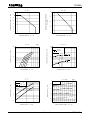
0.01
0.1
1
10
1 10 100
1
10
100
1 10 100
1
10
100
0.9 1 1.1 1.2 1.3 1.4 1.5
0
0.5
1
1.5
2
2.5
3
3.5
4
024681012
0
20
40
60
80
0 20406080100
0
5
10
15
20
25
30
35
0 20406080100
I
F
– Ta
Ambient temperature Ta (°C)
Allowable forward current I
F
(mA)
I
F
– V
F
(typ.
)
Forward voltage V
F
(V)
Forward current I
F
(mA)
0
Ta = 75°C
50
25
−25
I
C
– I
F
Forward current I
F
(mA)
Collector current I
C
(mA)
Ta = 25°C
V
CE
= 2V
V
CE
= 0.4V
Sample 1
Sample 2
I
C
/ I
F
– I
F
Forward current I
F
(mA)
Current transfer ratio I
C
/I
F
(%)
Ta = 25°C
V
CE
= 2V
V
CE
= 0.4V
Sample 2
Sample 1
I
C
– V
CE
(typ.)
Collector-emitter voltage V
CE
(V)
Collector current I
C
(mA)
20
I
F
= 5mA
10
15
Ta = 25°C
P
C
– Ta
Ambient temperature Ta (°C)
Allowable collector power dissipation
P
C
(mW)

TLP848
2007-10-01
10
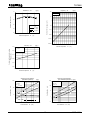
1
10
100
1000
110100
0.00
0.04
0.08
0.12
0.16
0.20
-40 -20 0 20 40 60 80 100
0.1
1
10
100
1000
0.1 1 10 100
0.00001
0.0001
0.001
0.01
0.1
1
10
100
0 20 40 60 80 100 120
0.2
0.4
0.6
0.8
1
1.2
-40 -20 0 20 40 60 80 100
Relative I
C
– Ta (typ.)
Ambient temperature Ta (°C)
Relative collector current
V
CE
= 2V
I
F
= 20mA
I
F
= 10mA
I
F
= 5mA
V
CE (sat)
– Ta (typ.)
Ambient temperature Ta (°C)
Collector-emitter saturation voltage
V
CE(sat) (V)
I
C
= 0.15mA
I
F
= 10mA
Switching characteristics
(saturated operation) (typ.)
Load resistance R
L
(kΩ)
Switching time (μs)
Ta = 25°C
I
F
= 20mA
V
CC
= 5V
V
OUT
≧ 4.65V
t
r
t
s
t
f
t
d
Switching characteristics
(non saturated operation) (typ.)
Load resistance R
L
(kΩ)
Switching time (μs)
t
r,
t
f
t
d
t
s
Ta = 25°C
V
CC
= 5V
V
OUT
= 1V
I
D
(I
CEO
) – Ta (typ.)
Ambient temperature Ta (°C)
Dark current I
D
(I
CEO
) (μA)
V
CE
= 12V

TLP848
2007-10-01
11
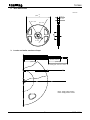
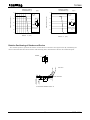
Relative Positioning of Shutter and Device
For normal operation, position the shutter and the device as shown in the figure below. By considering the
device's detection direction characteristic and switching time, determine the shutter slit width and pitch.
0
0.2
0.4
0.6
0.8
1
1.2
-2 -1 0 1 2 3 4
0
0.2
0.4
0.6
0.8
1
1.2
-1.2 -0.8 -0.4 0 0.4 0.8 1.2
Detection position
characteristics (1) (typ.)
Distance d (mm)
Relative collector current
Detection position
characteristics (2) (typ.)
Distance d (mm)
Relative collector current
I
F
= 5mA
V
CE
= 2V
Ta = 25°C
Detection position
d = 0 ± 0.2mm
0
d
Shutter
+−
I
F
= 5mA
V
CE
= 2V
Ta = 25°C
Detection position
d = 0.75 mm
Shutter
d
+0.6
-0.5
1.35 min
0.75
0.25 max
Center of sensor
Unit: mm
Cross section between A and A'
A
A
’
Shutte
r

TLP848
2007-10-01
12
RESTRICTIONS ON PRODUCT USE
20070701-EN
• The information contained herein is subject to change without notice.
• TOSHIBA is continually working to improve the quality and reliability of its products. Nevertheless, semiconductor
devices in general can malfunction or fail due to their inherent electrical sensitivity and vulnerability to physical
stress. It is the responsibility of the buyer, when utilizing TOSHIBA products, to comply with the standards of
safety in making a safe design for the entire system, and to avoid situations in which a malfunction or failure of
such TOSHIBA products could cause loss of human life, bodily injury or damage to property.
In developing your designs, please ensure that TOSHIBA products are used within specified operating ranges as
set forth in the most recent TOSHIBA products specifications. Also, please keep in mind the precautions and
conditions set forth in the “Handling Guide for Semiconductor Devices,” or “TOSHIBA Semiconductor Reliability
Handbook” etc.
• The TOSHIBA products listed in this document are intended for usage in general electronics applications
(computer, personal equipment, office equipment, measuring equipment, industrial robotics, domestic appliances,
etc.).These TOSHIBA products are neither intended nor warranted for usage in equipment that requires
extraordinarily high quality and/or reliability or a malfunction or failure of which may cause loss of human life or
bodily injury (“Unintended Usage”). Unintended Usage include atomic energy control instruments, airplane or
spaceship instruments, transportation instruments, traffic signal instruments, combustion control instruments,
medical instruments, all types of safety devices, etc.. Unintended Usage of TOSHIBA products listed in his
document shall be made at the customer’s own risk.
• The products described in this document shall not be used or embedded to any downstream products of which
manufacture, use and/or sale are prohibited under any applicable laws and regulations.
• The information contained herein is presented only as a guide for the applications of our products. No
responsibility is assumed by TOSHIBA for any infringements of patents or other rights of the third parties which
may result from its use. No license is granted by implication or otherwise under any patents or other rights of
TOSHIBA or the third parties.
• GaAs(Gallium Arsenide) is used in this product. The dust or vapor is harmful to the human body. Do not break,
cut, crush or dissolve chemically.
• Please contact your sales representative for product-by-product details in this document regarding RoHS
compatibility. Please use these products in this document in compliance with all applicable laws and regulations
that regulate the inclusion or use of controlled substances. Toshiba assumes no liability for damage or losses
occurring as a result of noncompliance with applicable laws and regulations.
-
 1
1
-
 2
2
-
 3
3
-
 4
4
-
 5
5
-
 6
6
-
 7
7
-
 8
8
-
 9
9
-
 10
10
-
 11
11
-
 12
12


Ask a question and I''ll find the answer in the document
Finding information in a document is now easier with AI
Other documents
-
NXP Semiconductors PBLS4004D User manual
-
Omron EE-SX1107 User manual
-
Panasonic 2SA2078G User manual
-
-
-
-
-
-
-