
Intel
®
Celeron
®
M Processor
Datasheet
June 2004
Order Number: 300302-003

2 Intel® Celeron® M Processor Datasheet
IINFORMATION IN THIS DOCUMENT IS PROVIDED IN CONNECTION WITH INTEL® PRODUCTS. NO LICENSE, EXPRESS OR IMPLIED, BY
ESTOPPEL OR OTHERWISE, TO ANY INTELLECTUAL PROPERTY RIGHTS IS GRANTED BY THIS DOCUMENT. EXCEPT AS PROVIDED IN
INTEL'S TERMS AND CONDITIONS OF SALE FOR SUCH PRODUCTS, INTEL ASSUMES NO LIABILITY WHATSOEVER, AND INTEL DISCLAIMS
ANY EXPRESS OR IMPLIED WARRANTY, RELATING TO SALE AND/OR USE OF INTEL PRODUCTS INCLUDING LIABILITY OR WARRANTIES
RELATING TO FITNESS FOR A PARTICULAR PURPOSE, MERCHANTABILITY, OR INFRINGEMENT OF ANY PATENT, COPYRIGHT OR OTHER
INTELLECTUAL PROPERTY RIGHT. Intel products are not intended for use in medical, life saving, life sustaining applications.
Intel may make changes to specifications and product descriptions at any time, without notice.
Designers must not rely on the absence or characteristics of any features or instructions marked "reserved" or "undefined." Intel reserves these for
future definition and shall have no responsibility whatsoever for conflicts or incompatibilities arising from future changes to them.
The Intel® Celeron® M Processor may contain design defects or errors known as errata which may cause the product to deviate from published
specifications. Current characterized errata are available on request.
Contact your local Intel sales office or your distributor to obtain the latest specifications and before placing your product order.
Copies of documents which have an order number and are referenced in this document, or other Intel literature, may be obtained by calling 1-800-
548-4725, or by visiting Intel's Web Site.
Intel, Intel logo, Celeron, and MMX are registered trademarks or trademarks of Intel Corporation or its subsidiaries in the United States and other
countries.
*Other names and brands may be claimed as the property of others.
Copyright © 2004, Intel Corporation

Intel
®
Celeron
®
M Processor Datasheet 3
Contents
1 Introduction ...................................................................................................................... 7
1.1 Terminology ........................................................................................................... 8
1.2 References.............................................................................................................9
1.3 State of Data ..........................................................................................................9
2 Low Power Features ......................................................................................................11
2.1 Clock Control and Low Power States...................................................................11
2.1.1 Normal State ........................................................................................... 11
2.1.2 AutoHALT Power-Down State.................................................................11
2.1.3 Stop-Grant State .....................................................................................12
2.1.4 HALT/Grant Snoop State ........................................................................12
2.1.5 Sleep State..............................................................................................12
2.1.6 Deep Sleep State ....................................................................................13
2.2 FSB Low Power Enhancements ..........................................................................13
2.3 Processor Power Status Indicator (PSI#) Signal..................................................14
3 Electrical Specifications ................................................................................................15
3.1 FSB and GTLREF................................................................................................15
3.2 Power and Ground Pins....................................................................................... 15
3.3 Decoupling Guidelines .........................................................................................15
3.3.1 VCC
Decoupling ...................................................................................... 16
3.3.2 FSB AGTL+ Decoupling ..........................................................................16
3.3.3 FSB Clock (BCLK[1:0]) and Processor Clocking.....................................16
3.4 Voltage Identification............................................................................................16
3.5 Catastrophic Thermal Protection.......................................................................... 17
3.6 Signal Terminations and Unused Pins .................................................................18
3.7 FSB Signal Groups .............................................................................................. 18
3.8 CMOS Signals .....................................................................................................19
3.9 Maximum Ratings ................................................................................................20
3.10 Processor DC Specifications................................................................................ 20
4 Package Mechanical Specifications and Pin Information ..........................................29
4.1 Processor Pin-Out and Pin List ............................................................................37
4.2 Alphabetical Signals Reference ...........................................................................56
5 Thermal Specifications and Design Considerations .................................................. 63
5.1 Thermal Specifications.........................................................................................65
5.1.1 Thermal Diode.........................................................................................65
5.1.2 Intel Thermal Monitor ..............................................................................66
6 Debug Tools Specifications ..........................................................................................69
6.1 Logic Analyzer Interface (LAI)............................................................................. 69
6.1.1 Mechanical Considerations .....................................................................69
6.1.2 Electrical Considerations.........................................................................69

4 Intel
®
Celeron
®
M Processor Datasheet
Figures
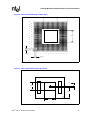
1 Clock Control States...................................................................................................................11
2 Illustration of Active State VCC Static and Ripple Tolerances ...................................................22
3 Illustration of Deep Sleep VCC Static and Ripple Tolerances....................................................24
4 Micro-FCPGA Package Top and Bottom Isometric Views .........................................................29
5 Micro-FCPGA Package - Top and Side Views ...........................................................................30
6 Micro-FCPGA Package - Bottom View .......................................................................................31
7 Intel Celeron M Processor Die Offset .........................................................................................31
8 Micro-FCBGA Package Top and Bottom Isometric Views .........................................................33
9 Micro-FCBGA Package Top and Side Views .............................................................................34
10 Micro-FCBGA Package Bottom View .........................................................................................35
11 The Coordinates of the Processor Pins as Viewed From the Top of the
Package......................................................................................................................................38

Intel
®
Celeron
®
M Processor Datasheet 5
Tables
1 References ................................................................................................................................9
2 Voltage Identification Definition ...............................................................................................17
3 FSB Pin Groups.......................................................................................................................19
4 Processor DC Absolute Maximum Ratings..............................................................................20
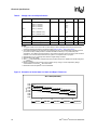
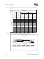
5 Voltage and Current Specifications .........................................................................................21
6 Voltage Tolerances for Intel Celeron M Processor with VID = 1.356 V
(Active State) ...........................................................................................................................23
7 Voltage Tolerances for Intel Celeron M Processor with VID = 1.356 V
(Deep Sleep State) ..................................................................................................................24
8 Voltage Tolerances for ULV Intel Celeron M Processor with VID = 1.004 V
(Active State) ...........................................................................................................................25
9 Voltage Tolerances for ULV Intel Celeron M Processor with VID = 1.004 V
(Deep Sleep State) ..................................................................................................................26
10 FSB Differential BCLK Specifications ......................................................................................26
11 AGTL+ Signal Group DC Specifications ..................................................................................27
12 CMOS Signal Group DC Specifications...................................................................................27
13 Open Drain Signal Group DC Specifications ...........................................................................28
14 Micro-FCPGA Package Dimensions........................................................................................32
15 Micro-FCBGA Package Dimensions........................................................................................36
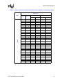
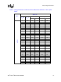
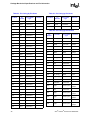
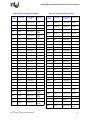
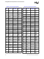
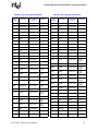
23 Pin Listing by Pin Name...........................................................................................................39
24 Pin Listing by Pin Number .......................................................................................................46
25 Signal Description....................................................................................................................56
26 Power Specifications for the Intel Celeron M Processor .........................................................64
27 Thermal Diode Interface ..........................................................................................................65
28 Thermal Diode Specifications ..................................................................................................65

6 Intel
®
Celeron
®
M Processor Datasheet
Revision History
Revision
Order
Number
Description Date
-001 300302 Initial release January 2004
-002 300302
• Added ULV 900 MHz and 1.40 GHz specs
• Updated DINV[3:0]# and BPM3# pin direction
April 2004
-003 300302 • Added 1.50 GHz specifications June 2004

Intel
®
Celeron
®
M Processor Datasheet 7
Introduction
1 Introduction
The Intel
®
Celeron
®
M processor and the ultra low voltage (ULV) Intel
®
Celeron
®
M processor
are high-performance, low-power mobile processors with several microarchitectural enhancements
over existing mobile Intel Celeron processors.
The Intel Celeron M processor is available at the following core frequencies in the Micro-FCBGA
and Micro-FCPGA packaging technologies:
• 1.20 GHz (1.356 V)
• 1.30 GHz (1.356 V)
• 1.40 GHz (1.356 V)
• 1.50 GHz (1.356 V)
The ultra low voltage Intel Celeron M processor is available at the following frequency in the
Micro-FCBGA packaging technology:
• 800 MHz (1.004 V)
• 900 MHz (1.004 V)
The Micro-FCPGA package plugs into a 479-hole, surface-mount, zero insertion force (ZIF)
socket, which is referred to as the mPGA479M socket.
The following list provides some of the key features of this processor:
• Supports Intel architecture with dynamic execution
• Manufactured on Intel’s advanced 0.13 micron process technology with copper interconnect.
• High-performance, low-power core featuring architectural innovations like micro-ops fusion
and advanced stack management that reduce the number of micro-ops handled by the
processor.
• On-die, primary 32-kB instruction cache and 32-kB, write-back, data cache
• On-die, 512-kB second level cache with Advanced Transfer Cache architecture
• Advanced branch prediction and data prefetch logic
• Streaming SIMD extensions 2 (SSE2) that enables breakthrough levels of performance in
multimedia applications including 3D graphics, video decoding/encoding, and speech
recognition.
• 400-MHz, source-synchronous front side bus (FSB)
• Advanced power management features
• Maintained support for MMX
TM
technology
• Compatible with IA-32 software.
The processor also features a very advanced branch prediction architecture that significantly
reduces the number of mispredicted branches. The processor’s Data Prefetch Logic speculatively
fetches data to the L2 cache before an L1 cache request occurs, resulting in reduced bus cycle
penalties and improved performance.

8 Intel
®
Celeron
®
M Processor Datasheet
Introduction
The new packed, double-precision, floating-point instructions enhance performance for
applications that require greater range and precision, including scientific and engineering
applications and advanced 3D geometry techniques, such as ray tracing.
The processor’s 400-MHz FSB utilizes a split-transaction, deferred reply protocol. The 400-MHz
FSB uses source-synchronous transfer (SST) of address and data to improve performance by
transferring data four times per bus clock (4X data transfer rate, as in AGP 4X). Along with the 4X
data bus, the address bus can deliver addresses two times per bus clock and is referred to as a
“double-clocked” or 2X address bus. Working together, the 4X data bus and 2X address bus
provide a data bus bandwidth of up to 3.2 GB/second. The FSB uses Advanced Gunning
Transceiver Logic (AGTL+) signal technology, a variant of GTL+ signalling technology with low
power enhancements.
Note: The term AGTL+ has been used for Assisted Gunning Transceiver Logic technology on other Intel
products.
1.1 Terminology
Term Definition
#
A “#” symbol after a signal name refers to an active low signal, indicating a signal is in the active
state when driven to a low level. For example, when RESET# is low, a reset has been requested.
Conversely, when NMI is high, a nonmaskable interrupt has occurred. In the case of signals where
the name does not imply an active state but describes part of a binary sequence (such as address
or data), the “#” symbol implies that the signal is inverted. For example, D[3:0] = “HLHL” refers to a
hex “A”, and D[3:0]# = “LHLH” also refers to a hex “A” (H= High logic level, L= Low logic level).
FSB
Front Side Bus refers to the interface between the processor and system core logic (also known as
the chipset components).

Intel
®
Celeron
®
M Processor Datasheet 9
Introduction
1.2 References
The following documents may be beneficial when reading this document. Please note that
“platform design guides,” when used throughout this document, refer to the following documents:
• Intel
852GM Chipset Platform Design Guide
• Intel
855GM/855GME Chipset Platform Design Guide
• Intel
855PM Chipset Platform Design Guide
NOTE: Contact your Intel representative for the latest revision and order number of this document.
1.3 State of Data
The data contained within this document represents the most accurate information available by the
publication date. However, all data in this document is preliminary and subject to change.
§
Table 1. References
Document Order Number
1
Intel
855PM Chipset Platform Design Guide http://developer.intel.com
Intel
855PM Chipset Design Guide Update http://developer.intel.com
Intel
855PM Chipset Datasheet http://developer.intel.com
IIntel
855GM/855GME Chipset Platform Design Guide http://developer.intel.com
Intel
855GM/855GME Chipset Datasheet http://developer.intel.com
Intel
855GM Specification Update http://developer.intel.com
Intel
852GM Chipset Datasheet http://developer.intel.com
Intel
Architecture Software Developer's Manual
http://developer.intel.com
Volume 1: Basic Architecture 253665
Volume 2A: Instruction Set Reference 253666
Volume 2B: Instruction Set Reference 253667
Volume 3: System Programming Guide 253668
ITP700 Debug Port Design Guide
http://developer.intel.com

10 Intel
®
Celeron
®
M Processor Datasheet
Introduction

Intel
®
Celeron
®
M Processor Datasheet 11
Low Power Features
2 Low Power Features
2.1 Clock Control and Low Power States
The Intel
Celeron M processor supports the AutoHALT, Stop Grant, Sleep, and Deep Sleep states
for optimal power management. See Figure 1 for a visual representation of the processor low-
power states.
2.1.1 Normal State
This is the normal operating state for the processor.
2.1.2 AutoHALT Power-Down State
AutoHALT is a low-power state entered when the processor executes the HALT instruction. The
processor will transition to the Normal state upon the occurrence of SMI#, INIT#, LINT[1:0]
(NMI, INTR), or FSB interrupt message. RESET# will cause the processor to immediately
initialize itself.
The return from a System Management Interrupt (SMI) handler can be to either Normal mode or
the AutoHALT Power-Down state. See the Intel Architecture Software Developer's Manual,
Volume III: System Programmer's Guide for more information.
Figure 1. Clock Control States
snoop
occurs
Stop
Grant
Normal Sleep
HALT/
Grant
Snoop
Auto Halt
Deep
Sleep
STPCLK# asserted
SLP# asserted
SLP# de-asserted
STPCLK# de-asserted
snoop
serviced
HLT
instruction
snoop
serviced
snoop
occurs
DPSLP#
de-asserted
DPSLP#
asserted
STPCLK#
asserted
STPCLK#
de-asserted
halt
break
V0001-04
Halt break - A20M#, INIT#, INTR, NMI, PREQ#, RESET#, SMI#, or APIC interrupt

12 Intel
®
Celeron
®
M Processor Datasheet
Low Power Features
The system can generate a STPCLK# while the processor is in the AutoHALT Power-Down state.
When the system deasserts the STPCLK# interrupt, the processor will return execution to the
HALT state.
While in AutoHALT Power-Down state, the processor will process bus snoops.
2.1.3 Stop-Grant State
When the STPCLK# pin is asserted, the Stop-Grant state of the processor is entered 20 bus clocks
after the response phase of the processor issued Stop-Grant Acknowledge special bus cycle.
Since the AGTL+ signal pins receive power from the FSB, these pins should not be driven
(allowing the level to return to V
CCP
) for minimum power drawn by the termination resistors in this
state. In addition, all other input pins on the FSB should be driven to the inactive state.
RESET# will cause the processor to immediately initialize itself, but the processor will stay in
Stop-Grant state. A transition back to the Normal state will occur with the deassertion of the
STPCLK# signal. When re-entering the Stop-Grant state from the Sleep state, STPCLK# should be
deasserted ten or more bus clocks after the deassertion of SLP#.
A transition to the HALT/Grant Snoop state will occur when the processor detects a snoop on the
FSB (see Section 2.1.4). A transition to the Sleep state (see Section 2.1.5) will occur with the
assertion of the SLP# signal.
While in the Stop-Grant State, SMI#, INIT# and LINT[1:0] will be latched by the processor, and
only serviced when the processor returns to the Normal State. Only one occurrence of each event
will be recognized upon return to the Normal state. Please refer to the FERR# pin description in
Section 4.2 for details on FERR# break event behavior in the Stop Grant state.
While in Stop-Grant state, the processor will process snoops on the FSB and it will latch interrupts
delivered on the FSB.
The PBE# signal can be driven when the processor is in Stop-Grant state. PBE# will be asserted if
there is any pending interrupt latched within the processor. Pending interrupts that are blocked by
the EFLAGS.IF bit being clear will still cause assertion of PBE#. Assertion of PBE# indicates to
system logic that it should return the processor to the Normal state.
2.1.4 HALT/Grant Snoop State
The processor will respond to snoop or interrupt transactions on the FSB while in Stop-Grant state
or in AutoHALT Power-Down state. During a snoop or interrupt transaction, the processor enters
the HALT/Grant Snoop state. The processor will stay in this state until the snoop on the FSB has
been serviced (whether by the processor or another agent on the FSB) or the interrupt has been
latched. After the snoop is serviced or the interrupt is latched, the processor will return to the Stop-
Grant state or AutoHALT Power-Down state, as appropriate.
2.1.5 Sleep State
The Sleep state is a low-power state in which the processor maintains its context, maintains the
phase-locked loop (PLL), and has stopped all internal clocks. The Sleep state can only be entered
from Stop-Grant state. Once in the Stop-Grant state, the processor will enter the Sleep state upon

Intel
®
Celeron
®
M Processor Datasheet 13
Low Power Features
the assertion of the SLP# signal. The SLP# pin should only be asserted when the processor is in the
Stop Grant state. SLP# assertions while the processor is not in the Stop-Grant state is out of
specification and may result in unapproved operation.
Snoop events that occur while in Sleep State or during a transition into or out of Sleep state will
cause unpredictable behavior.
In the Sleep state, the processor is incapable of responding to snoop transactions or latching
interrupt signals. No transitions or assertions of signals (with the exception of SLP#, DPSLP# or
RESET#) are allowed on the FSB while the processor is in Sleep state. Any transition on an input
signal before the processor has returned to Stop-Grant state will result in unpredictable behavior.
If RESET# is driven active while the processor is in the Sleep state, and held active as specified in
the RESET# pin specification, then the processor will reset itself, ignoring the transition through
Stop-Grant State. If RESET# is driven active while the processor is in the Sleep State, the SLP#
and STPCLK# signals should be deasserted immediately after RESET# is asserted to ensure the
processor correctly executes the Reset sequence.
While in the Sleep state, the processor is capable of entering an even lower power state, the Deep
Sleep state by asserting the DPSLP# pin. (see Section 2.1.6.). While the processor is in the Sleep
state, the SLP# pin must be deasserted if another asynchronous FSB event needs to occur.
2.1.6 Deep Sleep State
Deep Sleep state is a very low-power state the processor can enter while maintaining context. Deep
Sleep state is entered by asserting the DPSLP# pin while in the Sleep state. BCLK may be stopped
during the Deep Sleep state for additional platform-level power savings. BCLK stop/restart timings
on Intel 855PM/ICH4-M, Intel 855GM/ICH4-M, and Intel 852GM/ICH4-M chipset-based
platforms with the CK-408 clock chip are as follows:
• Deep Sleep entry - DPSLP# and CPU_STP# are asserted simultaneously. CK-408 will stop/
tristate BCLK within 2 BCLKs +/- a few nanoseconds.
• Deep Sleep exit - DPSLP# and CPU_STP# are deasserted simultaneously. CK-408 will drive
BCLK to differential DC levels within 2-3 ns and starts toggling BCLK 2-6 BCLK periods
later.
To re-enter the Sleep state, the DPSLP# pin must be deasserted. BCLK can be restarted after
DPSLP# deassertion as described above. A period of 30 microseconds (to allow for PLL
stabilization) must occur before the processor can be considered to be in the Sleep State. Once in
the Sleep state, the SLP# pin must be deasserted to re-enter the Stop-Grant state.
While in Deep Sleep state, the processor is incapable of responding to snoop transactions or
latching interrupt signals. No transitions of signals are allowed on the FSB while the processor is in
Deep Sleep state. Any transition on an input signal before the processor has returned to Stop-Grant
state will result in unpredictable behavior.
When the processor is in Deep Sleep state, it will not respond to interrupts or snoop transactions.
2.2 FSB Low Power Enhancements
The Intel Celeron M processor incorporates the following FSB low power enhancements:
• Dynamic FSB power-down

14 Intel
®
Celeron
®
M Processor Datasheet
Low Power Features
• BPRI# control for address and control input buffers
• Dynamic on-die termination disabling
• Low VCCP (I/O termination voltage)
The Intel Celeron M processor incorporates the DPWR# signal that controls the data bus input
buffers on the processor. The DPWR# signal disables the buffers when not used and activates
them only when data bus activity occurs, resulting in significant power savings with no
performance impact. BPRI# control also allows the processor address and control input buffers to
be turned off when the BPRI# signal is inactive. The On-Die termination on the processor FSB
buffers is disabled when the signals are driven low, resulting in additional power savings. The low
I/O termination voltage is on a dedicated voltage plane independent of the core voltage, enabling
low I/O switching power at all times.
2.3 Processor Power Status Indicator (PSI#) Signal
The Intel Celeron M processor incorporates the PSI# signal that is asserted when the processor is in
a low power (Deep Sleep ) state. This signal is asserted upon Deep Sleep entry and deasserted upon
exit. PSI# can be used to improve the light load efficiency of the voltage regulator, resulting in
platform power savings and extended battery life.

Intel
®
Celeron
®
M Processor Datasheet 15
Electrical Specifications
3 Electrical Specifications
3.1 FSB and GTLREF
The Intel
Celeron M processor FSB uses Advanced Gunning Transceiver Logic (AGTL+)
signalling technology, a variant of GTL+ signalling technology with low power enhancements.
This signalling technology provides improved noise margins and reduced ringing through low-
voltage swings and controlled edge rates. The termination voltage level for the Intel Celeron M
processor AGTL+ signals is VCCP
= 1.05 V (nominal). Due to speed improvements to data and
address bus, signal integrity and platform design methods have become more critical than with
previous processor families. Design guidelines for the Intel Celeron M processor FSB will be
detailed in the platform design guides.
The AGTL+ inputs require a reference voltage (GTLREF) that is used by the receivers to determine
if a signal is a logical 0 or a logical 1. GTLREF must be generated on the system board.
Termination resistors are provided on the processor silicon and are terminated to its I/O voltage
(VCCP). Intel’s 855PM, 855GM, and 852GM chipsets will also provide on-die termination, thus
eliminating the need to terminate the bus on the system board for most AGTL+ signals.
Refer to the platform design guides for board level termination resistor requirements.
The AGTL+ bus depends on incident wave switching. Therefore, timing calculations for AGTL+
signals are based on flight time as opposed to capacitive deratings. Analog signal simulation of the
FSB, including trace lengths, is highly recommended when designing a system.
3.2 Power and Ground Pins
For clean on-chip power distribution, the Intel Celeron M processor will have a large number of
V
CC
(power) and V
SS
(ground) inputs. All power pins must be connected to V
CC
power planes while
all V
SS
pins must be connected to system ground planes. Use of multiple power and ground planes
is recommended to reduce I x R drop. Please refer to the platform design guides for more details.
The processor V
CC
pins must be supplied the voltage determined by the VID (Voltage ID) pins.
3.3 Decoupling Guidelines
Due to its large number of transistors and high internal clock speeds, the processor is capable of
generating large average current swings between low- and full-power states. This may cause
voltages on power planes to sag below their minimum values if bulk decoupling is not adequate.
Care must be taken in the board design to ensure that the voltage provided to the processor remains
within the specifications listed in Table 5. Failure to do so can result in timing violations or
reduced lifetime of the component. For further information and design guidelines, refer to the
platform design guides.

16 Intel
®
Celeron
®
M Processor Datasheet
Electrical Specifications
3.3.1 V
CC
Decoupling
Regulator solutions need to provide bulk capacitance with a low effective series resistance (ESR)
and keep a low interconnect resistance from the regulator to the socket. Bulk decoupling for the
large current swings when the part is powering on, or entering/exiting low-power states, must be
provided by the voltage regulator solution. For more details on decoupling recommendations,
please refer to the platform design guides. Intel strongly recommends that the layout and
decoupling recommendations in the platform design guides be followed.
3.3.2 FSB AGTL+ Decoupling
Intel
Celeron M processors integrate signal termination on the die as well as incorporate high-
frequency decoupling capacitance on the processor package. Decoupling must also be provided by
the system motherboard for proper AGTL+ bus operation. For more information, refer to the
platform design guides.
3.3.3 FSB Clock (BCLK[1:0]) and Processor Clocking
BCLK[1:0] directly controls the FSB interface speed as well as the core frequency of the processor.
As in previous generation processors, the Intel Celeron M processor core frequency is a multiple of
the BCLK[1:0] frequency. In regards to processor clocking, the Intel Celeron M processor uses a
differential clocking implementation.
3.4 Voltage Identification
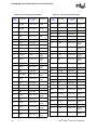
The processor uses six voltage identification pins, VID[5:0], to support automatic selection of
power supply voltages. The VID pins for the processor are CMOS outputs driven by the processor
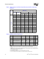
VID circuitry. Table 2 specifies the voltage level corresponding to the state of VID[5:0]. A 1 in this
refers to a high-voltage level and a 0 refers to low-voltage level.

Intel
®
Celeron
®
M Processor Datasheet 17
Electrical Specifications
Table 2. Voltage Identification Definition
3.5 Catastrophic Thermal Protection
The processor supports the THERMTRIP# signal for catastrophic thermal protection. An external
thermal sensor should also be used to protect the processor and the system against excessive
temperatures. Even with the activation of THERMTRIP#, which halts all processor internal clocks
and activity, leakage current can be high enough such that the processor cannot be protected in all
conditions without the removal of power to the processor. If the external thermal sensor detects a
catastrophic processor temperature of 125 °C (maximum), or if the THERMTRIP# signal is
asserted, the VCC supply to the processor must be turned off within
500 ms to prevent permanent silicon damage due to thermal runaway of the processor.
VID VID
5 4 3 2 1 0
V
CC
V
5 4 3 2 1 0
V
CC
V
0 0 0 0 0 0 1.708 1 0 0 0 0 0 1.196
0 0 0 0 0 1 1.692 1 0 0 0 0 1 1.180
0 0 0 0 1 0 1.676 1 0 0 0 1 0 1.164
0 0 0 0 1 1 1.660 1 0 0 0 1 1 1.148
0 0 0 1 0 0 1.644 1 0 0 1 0 0 1.132
0 0 0 1 0 1 1.628 1 0 0 1 0 1 1.116
0 0 0 1 1 0 1.612 1 0 0 1 1 0 1.100
0 0 0 1 1 1 1.596 1 0 0 1 1 1 1.084
0 0 1 0 0 0 1.580 1 0 1 0 0 0 1.068
0 0 1 0 0 1 1.564 1 0 1 0 0 1 1.052
0 0 1 0 1 0 1.548 1 0 1 0 1 0 1.036
0 0 1 0 1 1 1.532 1 0 1 0 1 1 1.020
0 0 1 1 0 0 1.516 1 0 1 1 0 0 1.004
0 0 1 1 0 1 1.500 1 0 1 1 0 1 0.988
0 0 1 1 1 0 1.484 1 0 1 1 1 0 0.972
0 0 1 1 1 1 1.468 1 0 1 1 1 1 0.956
0 1 0 0 0 0 1.452 1 1 0 0 0 0 0.940
0 1 0 0 0 1 1.436 1 1 0 0 0 1 0.924
0 1 0 0 1 0 1.420 1 1 0 0 1 0 0.908
0 1 0 0 1 1 1.404 1 1 0 0 1 1 0.892
0 1 0 1 0 0 1.388 1 1 0 1 0 0 0.876
0 1 0 1 0 1 1.372 1 1 0 1 0 1 0.860
0 1 0 1 1 0 1.356 1 1 0 1 1 0 0.844
0 1 0 1 1 1 1.340 1 1 0 1 1 1 0.828
0 1 1 0 0 0 1.324 1 1 1 0 0 0 0.812
0 1 1 0 0 1 1.308 1 1 1 0 0 1 0.796
0 1 1 0 1 0 1.292 1 1 1 0 1 0 0.780
0 1 1 0 1 1 1.276 1 1 1 0 1 1 0.764
0 1 1 1 0 0 1.260 1 1 1 1 0 0 0.748
0 1 1 1 0 1 1.244 1 1 1 1 0 1 0.732
0 1 1 1 1 0 1.228 1 1 1 1 1 0 0.716
0 1 1 1 1 1 1.212 1 1 1 1 1 1 0.700

18 Intel
®
Celeron
®
M Processor Datasheet
Electrical Specifications
3.6 Signal Terminations and Unused Pins
All RSVD (RESERVED) pins must remain unconnected. Connection of these pins to V
CC
, V
SS
, or
to any other signal (including each other) can result in component malfunction or incompatibility
with future Intel Celeron M processors. See Section 4.1 for a pin listing of the processor and the
location of all RSVD pins.
For reliable operation, always connect unused inputs or bidirectional signals to an appropriate
signal level. Unused active low AGTL+ inputs may be left as no connects if AGTL+ termination is
provided on the processor silicon. Unused active high inputs should be connected through a resistor
to ground (V
SS
). Unused outputs can be left unconnected.
For details on signal terminations, please refer to the platform design guides. TAP signal
termination requirements are also discussed in
ITP700 Debug Port Design Guide.
The TEST1, TEST2, and TEST3 pins must be left unconnected but should have a stuffing option
connection to V
SS
separately via 1-kΩ, pull-down resistors.
3.7 FSB Signal Groups
In order to simplify the following discussion, the FSB signals have been combined into groups by
buffer type. AGTL+ input signals have differential input buffers, which use GTLREF as a reference
level. In this document, the term "AGTL+ Input" refers to the AGTL+ input group as well as the
AGTL+ I/O group when receiving. Similarly, "AGTL+ Output" refers to the AGTL+ output group
as well as the AGTL+ I/O group when driving.
With the implementation of a source synchronous data bus comes the need to specify two sets of
timing parameters. One set is for common clock signals which are dependant upon the crossing of
the rising edge of BCLK0 and the falling edge of BCLK1. The second set is for the source
synchronous signals which are relative to their respective strobe lines (data and address) as well as
the rising edge of BCLK0. Asychronous signals are still present (A20M#, IGNNE#, etc.) and can
become active at any time during the clock cycle. Table 3 identifies which signals are common
clock, source synchronous, and asynchronous.

Intel
®
Celeron
®
M Processor Datasheet 19
Electrical Specifications
NOTES:
1. Refer to Chapter 4 for signal descriptions and termination requirements.
2. BPM[2:0]# and PRDY# are AGTL+ output only signals.
3. In processor systems where there is no debug port implemented on the system board, these signals are used
to support a debug port interposer. In systems with the debug port implemented on the system board, these
signals are no connects.
3.8 CMOS Signals
CMOS input signals are shown in Table 3. Legacy output FERR#, IERR# and other non-AGTL+
signals (THERMTRIP# and PROCHOT#) utilize Open Drain output buffers. These signals do not
have setup or hold time specifications in relation to BCLK[1:0]. However, all of the CMOS signals
are required to be asserted for at least three BCLKs in order for the chipset to recognize them. See
Section 3.10 for the DC specifications for the CMOS signal groups.
Table 3. FSB Pin Groups
Signal Group Type Signals
1
AGTL+ Common Clock Input
Synchronous
to BCLK[1:0]
BPRI#, DEFER#, DPWR#, PREQ#, RESET#, RS[2:0]#,
TRDY#
AGTL+ Common Clock I/O
Synchronous
to BCLK[1:0]
ADS#, BNR#, BPM[3:0]#
2
, BR0#, DBSY#, DRDY#, HIT#,
HITM#, LOCK#, PRDY#
2
AGTL+ Source Synchronous I/O
Synchronous
to assoc.
strobe
AGTL+ Strobes
Synchronous
to BCLK[1:0]
ADSTB[1:0]#, DSTBP[3:0]#, DSTBN[3:0]#
CMOS Input Asynchronous
A20M#, DPSLP#, IGNNE#, INIT#, LINT0/INTR, LINT1/
NMI, PWRGOOD, SMI#, SLP#, STPCLK#
Open Drain Output Asynchronous FERR#, IERR#, PROCHOT#, THERMTRIP#
CMOS Output Asynchronous PSI#, VID[5:0]
CMOS Input
Synchronous
to TCK
TCK, TDI, TMS, TRST#
Open Drain Output
Synchronous
to TCK
TDO
FSB Clock Clock BCLK[1:0], ITP_CLK[1:0]
3
Power/Other
COMP[3:0], DBR#
3
, GTLREF, RSVD, TEST3, TEST2,
TEST1, THERMDA, THERMDC, V
CC
, V
CCA
[3:0], V
CCP,
V
CCQ
[1:0], V
CC_SENSE
, V
SS,
V
SS_SENSE
Signals Associated Strobe
REQ[4:0]#, A[16:3]# ADSTB[0]#
A[31:17]# ADSTB[1]#
D[15:0]#, DINV0# DSTBP0#, DSTBN0#
D[31:16]#, DINV1# DSTBP1#, DSTBN1#
D[47:32]#, DINV2# DSTBP2#, DSTBN2#
D[63:48]#, DINV3# DSTBP3#, DSTBN3#

20 Intel
®
Celeron
®
M Processor Datasheet
Electrical Specifications
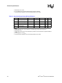
3.9 Maximum Ratings
Table 4 lists the processor’s maximum environmental stress ratings. The processor should not
receive a clock while subjected to these conditions. Functional operating parameters are listed in
the AC and DC tables. Extended exposure to the maximum ratings may affect device reliability.
Furthermore, although the processor contains protective circuitry to resist damage from electro
static discharge (ESD), system designers should always take precautions to avoid high-static
voltages or electric fields.
NOTES:
1. This rating applies to any processor pin.
2. Contact Intel for storage requirements in excess of one year.
3.10 Processor DC Specifications
The processor DC specifications in this section are defined at the processor core (pads) unless
noted otherwise
. See Table 11 for the pin signal definitions and signal pin assignments. Most of
the signals on the FSB are in the AGTL+ signal group. The DC specifications for these signals are
listed in Table 11. DC specifications for the CMOS group are listed in Table 12.
Table 5 through Table 13 list the DC specifications for the Intel Celeron M processor and are valid
only while meeting specifications for junction temperature, clock frequency, and input voltages.
Active Mode load line specifications apply in all states except in the Deep Sleep state. V
CC,BOOT
is
the default voltage driven by the voltage regulator at power up in order to set the VID values.
Unless specified otherwise, all specifications for the Intel Celeron M processor are at Tjunction =
100
°C. Care should be taken to read all notes associated with each parameter.
Table 4. Processor DC Absolute Maximum Ratings
Symbol Parameter Min Max Unit Notes
T
STORAGE Processor storage temperature –40 85 °C 2
V
CC
Any processor supply voltage with
respect to V
SS
-0.3 1.75 V 1
V
inAGTL+
AGTL+ buffer DC input voltage with
respect to V
SS
-0.1 1.75 V 1, 2
V
inAsynch_CMOS
CMOS buffer DC input voltage with
respect to V
SS
-0.1 1.75 V 1, 2
Page is loading ...
Page is loading ...
Page is loading ...
Page is loading ...
Page is loading ...
Page is loading ...
Page is loading ...
Page is loading ...
Page is loading ...
Page is loading ...
Page is loading ...
Page is loading ...
Page is loading ...
Page is loading ...
Page is loading ...
Page is loading ...
Page is loading ...
Page is loading ...
Page is loading ...
Page is loading ...
Page is loading ...
Page is loading ...
Page is loading ...
Page is loading ...
Page is loading ...
Page is loading ...
Page is loading ...
Page is loading ...
Page is loading ...
Page is loading ...
Page is loading ...
Page is loading ...
Page is loading ...
Page is loading ...
Page is loading ...
Page is loading ...
Page is loading ...
Page is loading ...
Page is loading ...
Page is loading ...
Page is loading ...
Page is loading ...
Page is loading ...
Page is loading ...
Page is loading ...
Page is loading ...
Page is loading ...
Page is loading ...
Page is loading ...
-
 1
1
-
 2
2
-
 3
3
-
 4
4
-
 5
5
-
 6
6
-
 7
7
-
 8
8
-
 9
9
-
 10
10
-
 11
11
-
 12
12
-
 13
13
-
 14
14
-
 15
15
-
 16
16
-
 17
17
-
 18
18
-
 19
19
-
 20
20
-
 21
21
-
 22
22
-
 23
23
-
 24
24
-
 25
25
-
 26
26
-
 27
27
-
 28
28
-
 29
29
-
 30
30
-
 31
31
-
 32
32
-
 33
33
-
 34
34
-
 35
35
-
 36
36
-
 37
37
-
 38
38
-
 39
39
-
 40
40
-
 41
41
-
 42
42
-
 43
43
-
 44
44
-
 45
45
-
 46
46
-
 47
47
-
 48
48
-
 49
49
-
 50
50
-
 51
51
-
 52
52
-
 53
53
-
 54
54
-
 55
55
-
 56
56
-
 57
57
-
 58
58
-
 59
59
-
 60
60
-
 61
61
-
 62
62
-
 63
63
-
 64
64
-
 65
65
-
 66
66
-
 67
67
-
 68
68
-
 69
69


