
PART NUMBER MOTOROLA
MANUAL TYPE -1
Motorola Microcontroller Family
SCIM
SINGLE-CHIP INTEGRATION
MODULE
Reference Manual
Frees
cale Semiconductor,
I
Freescale Semiconductor, Inc.
For More Information On This Product,
Go to: www.freescale.com
nc...

MOTOROLA PART NUMBER
-2 MANUAL TYPE
Frees
cale Semiconductor,
I
Freescale Semiconductor, Inc.
For More Information On This Product,
Go to: www.freescale.com
nc...

SCIM MOTOROLA
REFERENCE MANUAL iii
Paragraph Title Page
SECTION 1INTRODUCTION
1.1 SCIM Address Map ...................................................................................1-5
1.2 Bus Configuration and Reset Mode Selection ...........................................1-7
1.3 CPU-Specific Differences Affecting SCIM Operation ................................1-8
SECTION 2 SIGNAL AND PIN DESCRIPTIONS
2.1 Pin Characteristics ....................................................................................2-1
2.2 Signal Descriptions ....................................................................................2-2
SECTION 3 SYSTEM CONFIGURATION AND PROTECTION
3.1 Module Configuration and Testing ............................................................3-2
3.1.1 Module Mapping ................................................................................3-2
3.1.2 Privilege Levels .................................................................................3-2
3.1.3 Response to FREEZE Assertion .......................................................3-2
3.1.4 Interrupt Arbitration Priority ...............................................................3-3
3.1.5 Single-Chip Operation Support .........................................................3-3
3.1.6 Factory Test Mode ............................................................................3-3
3.1.7 SCIM Configuration Register .............................................................3-4
3.1.8 SCIM Test Registers .........................................................................3-5
3.2 Internal Bus Monitor ..................................................................................3-6
3.3 Halt Monitor ...............................................................................................3-6
3.4 Spurious Interrupt Monitor .........................................................................3-6
3.5 Software Watchdog ...................................................................................3-7
3.5.1 Software Watchdog Prescaling .........................................................3-7
3.5.2 Software Watchdog Divide Ratio .......................................................3-7
3.6 Periodic Interrupt Timer .............................................................................3-9
3.6.1 Prescaler and Modulus Counter ........................................................3-9
3.6.1.1 Pit Prescaling ..........................................................................3-10
3.6.1.2 Pit Period with a 32.768-kHz Reference Frequency ...............3-10
3.6.1.3 Pit Period with a 4.194-MHz Reference Frequency ................3-11
3.6.2 Pit Interrupt Priority and Vectoring ..................................................3-11
3.7 Low-Power Stop Operation .....................................................................3-12
3.8 System Protection Registers ...................................................................3-12
3.8.1 Software Service Register (SWSR) .................................................3-12
3.8.2 Periodic Interrupt Control Register (PICR) ......................................3-12
3.8.3 Periodic Interrupt Timer Register (PITR) .........................................3-13
3.8.4 System Protection Control Register (SYPCR) ................................3-13
SECTION 4 SYSTEM CLOCK
TABLE OF CONTENTS
Frees
cale Semiconductor,
I
Freescale Semiconductor, Inc.
For More Information On This Product,
Go to: www.freescale.com
nc...

MOTOROLA SCIM
iv REFERENCE MANUAL
(Continued)
Paragraph Title Page
TABLE OF CONTENTS
4.1 Clock Sources ...........................................................................................4-1
4.2 Clock Synthesizer Operation .....................................................................4-1
4.3 System Clock Frequency Control ..............................................................4-4
4.3.1 Frequency Control with a Reference Frequency of 25–50 kHz .........4-5
4.3.2 Frequency Control with a Reference Frequency of 3.2–6.4 MHz .....4-5
4.3.3 Avoiding Frequency Overshoot .........................................................4-5
4.3.4 Frequency Control Tables .................................................................4-6
4.4 External Circuit Design ............................................................................4-11
4.4.1 Conditioning the XTAL and EXTAL Pins .........................................4-11
4.4.2 Crystal Tune-Up Procedure .............................................................4-12
4.4.3 Conditioning the XFC, V
DDSYN
, and V
SSI
Pins ................................4-13
4.5 External Clock Signal Input .....................................................................4-14
4.6 External Bus Clock ..................................................................................4-14
4.7 System Clock and Low-Power Stop ........................................................4-14
4.8 Loss of Clock ...........................................................................................4-15
4.8.1 Loss of Reference Frequency .........................................................4-16
4.8.2 Loss of External Clock .....................................................................4-17
4.8.3 Loss-of-Clock Reset ........................................................................4-17
4.9 Clock Synthesizer Control Register (SYNCR) .........................................4-17
SECTION 5 EXTERNAL BUS INTERFACE
5.1 Bus Signal Descriptions ............................................................................5-2
5.1.1 Address Bus ......................................................................................5-2
5.1.2 Address Strobe ..................................................................................5-2
5.1.3 Data Bus ............................................................................................5-2
5.1.4 Data Strobe .......................................................................................5-2
5.1.5 Read/Write Signal .............................................................................5-2
5.1.6 Size Signals .......................................................................................5-2
5.1.7 Function Codes .................................................................................5-3
5.1.8 Data and Size Acknowledge Signals .................................................5-3
5.1.9 Bus Error Signal ................................................................................5-3
5.1.10 Halt Signal .........................................................................................5-3
5.1.11 Autovector Signal ..............................................................................5-4
5.2 External Bus Cycle Overview ....................................................................5-4
5.2.1 Bus Cycle Operation .........................................................................5-5
5.2.2 Synchronization to CLKOUT .............................................................5-5
5.3 Dynamic Bus Sizing ..................................................................................5-6
5.3.1 Size Signal Encoding ........................................................................5-6
5.3.2 Data and Size Acknowledge Signal Encoding ..................................5-7
5.3.3 Operand Alignment ...........................................................................5-7
5.3.4 Misaligned Operands ........................................................................5-8
Frees
cale Semiconductor,
I
Freescale Semiconductor, Inc.
For More Information On This Product,
Go to: www.freescale.com
nc...

SCIM MOTOROLA
REFERENCE MANUAL v
(Continued)
Paragraph Title Page
TABLE OF CONTENTS
5.3.5 Bus Sizing with a Partially Expanded Bus .........................................5-8
5.4 Data Transfer Operations ..........................................................................5-9
5.4.1 Read Cycles ......................................................................................5-9
5.4.2 Write Cycles ....................................................................................5-11
5.4.3 Indivisible Read-Modify-Write Sequence ........................................5-14
5.5 Operand Transfer Cases .........................................................................5-16
5.5.1 Byte Operand to 8-Bit Port ..............................................................5-17
5.5.2 Byte Operand to 16-Bit Port, Even (ADDR0 = 0) ............................5-18
5.5.3 Byte Operand to 16-Bit Port, Odd (ADDR0 = 1) ..............................5-18
5.5.4 Word Operand to 8-Bit Port, Aligned ...............................................5-19
5.5.5 Word Operand to 8-Bit Port, Misaligned ..........................................5-19
5.5.6 Word Operand to 16-Bit Port, Aligned .............................................5-20
5.5.7 Word Operand to 16-Bit Port, Misaligned ........................................5-21
5.5.8 Long-Word Operand to 8-Bit Port, Aligned ......................................5-21
5.5.9 Long-Word Operand to 8-Bit Port, Misaligned ................................5-24
5.5.10 Long-Word Operand to 16-Bit Port, Aligned ....................................5-25
5.5.11 Long-Word Operand to 16-Bit Port, Misaligned ..............................5-27
5.6 Function Codes and Memory Usage .......................................................5-28
5.7 System Interfacing Examples with External Chip Selects .......................5-29
5.7.1 Connecting an 8-Bit Memory Device to the MCU ............................5-29
5.7.2 Connecting a 16-Bit Memory Device to the MCU ............................5-30
5.7.3 Connecting Two 8-Bit Memory Devices to the MCU .......................5-31
5.8 CPU Space Cycles ..................................................................................5-32
5.8.1 Breakpoint Acknowledge Cycle .......................................................5-33
5.8.1.1 Software Breakpoints ..............................................................5-33
5.8.1.2 Hardware Breakpoints .............................................................5-34
5.8.2 LPSTOP Broadcast Cycle ...............................................................5-39
5.9 Bus Error Processing ..............................................................................5-39
5.9.1 Bus Error Exceptions .......................................................................5-41
5.9.2 Double Bus Faults ...........................................................................5-44
5.9.3 Retry Operation ...............................................................................5-45
5.9.4 Halt Operation .................................................................................5-47
5.10 Bus Arbitration .........................................................................................5-49
5.10.1 Bus Request ....................................................................................5-51
5.10.2 Bus Grant ........................................................................................5-51
5.10.3 Bus Grant Acknowledge ..................................................................5-52
5.10.4 Bus Arbitration Control ....................................................................5-52
5.10.5 Factory Test (Slave) Mode Arbitration .............................................5-54
5.11 Show Cycles ............................................................................................5-54
SECTION 6 INTERRUPTS
Frees
cale Semiconductor,
I
Freescale Semiconductor, Inc.
For More Information On This Product,
Go to: www.freescale.com
nc...

MOTOROLA SCIM
vi REFERENCE MANUAL
(Continued)
Paragraph Title Page
TABLE OF CONTENTS
6.1 Sources of Interrupt ...................................................................................6-1
6.2 Interrupt Level and Recognition ................................................................6-1
6.3 Interrupt Arbitration ....................................................................................6-2
6.4 Interrupt-Acknowledge Bus Cycles ...........................................................6-3
6.4.1 Bus Cycle Terminated by DSACK Signals ........................................6-5
6.4.2 Bus Cycle Terminated by AVEC Signal ............................................6-7
6.4.3 Spurious Interrupt Cycle ....................................................................6-9
6.5 Interrupt Processing Summary ................................................................6-10
SECTION 7 CHIP SELECTS
7.1 Chip-Select Options ..................................................................................7-2
7.2 Chip-Select Base Addresses .....................................................................7-4
7.3 Pin Assignments and Discrete Output .......................................................7-5
7.4 Chip-Select Operation ...............................................................................7-6
7.5 Chip-Select Timing ....................................................................................7-9
7.5.1 Synchronization with AS or DS .........................................................7-9
7.5.2 Wait States and DSACK Generation ...............................................7-10
7.5.3 Synchronization with ECLK .............................................................7-10
7.6 Chip Selects and Dynamic Bus Sizing ....................................................7-11
7.7 Fast Termination Cycles ..........................................................................7-11
7.7.1 Fast-Termination Read Cycle ..........................................................7-13
7.7.2 Fast-Termination Write Cycle ..........................................................7-14
7.8 Using Chip Selects in Interrupt-Acknowledge Cycles .............................7-14
7.8.1 Using a Chip-Select Pin as An Interrupt-Acknowledge Signal ........7-15
7.8.2 Generating An Autovector Signal with a Chip-Select Circuit ...........7-16
7.9 Emulation-Support Chip Selects .............................................................7-16
7.9.1 Port Emulation .................................................................................7-17
7.9.2 ROM Emulation ...............................................................................7-17
7.10 Chip-Select Reset Operation ...................................................................7-17
7.10.1 Pin Assignment ...............................................................................7-17
7.10.2 Chip-Select Base and Option Registers ..........................................7-18
7.10.3 CSBOOT Base and Option Registers .............................................7-18
7.11 Chip-Select Register Diagrams ...............................................................7-19
7.11.1 Chip-Select Pin Assignment Registers ............................................7-19
7.11.2 Chip-Select Base Address Registers ..............................................7-21
7.11.3 Chip-Select Option Registers ..........................................................7-21
7.11.4 Port C Data Register (PORTC) .......................................................7-24
7.12 Interfacing Example with SCIM Chip Selects ..........................................7-24
7.12.1 Configuring the RAM Chip Selects ..................................................7-25
7.12.1.1 Pin Connections ......................................................................7-25
7.12.1.2 Base Address Registers ..........................................................7-26
Frees
cale Semiconductor,
I
Freescale Semiconductor, Inc.
For More Information On This Product,
Go to: www.freescale.com
nc...

SCIM MOTOROLA
REFERENCE MANUAL vii
(Continued)
Paragraph Title Page
TABLE OF CONTENTS
7.12.1.3 Option Registers .....................................................................7-26
7.12.2 Configuring the Boot ROM Chip Select ...........................................7-26
7.12.2.1 Pin Connections ......................................................................7-26
7.12.2.2 Base Address Register ...........................................................7-27
7.12.2.3 Option Registers .....................................................................7-27
SECTION 8 RESET AND SYSTEM INITIALIZATION
8.1 Reset Operation ........................................................................................8-1
8.2 Sources of Reset .......................................................................................8-2
8.2.1 External Reset ...................................................................................8-3
8.2.2 Power-On Reset ................................................................................8-3
8.2.3 Software Watchdog Reset .................................................................8-3
8.2.4 HALT Reset .......................................................................................8-3
8.2.5 Loss-of-Clock Reset ..........................................................................8-3
8.2.6 System Reset ....................................................................................8-4
8.2.7 Test Module Reset ............................................................................8-4
8.2.8 Reset Status Register .......................................................................8-4
8.3 Reset Control Flow ....................................................................................8-5
8.3.1 RESET Assertion by an External Device ..........................................8-6
8.3.2 Internal Reset Request ......................................................................8-6
8.4 Power-On Reset ........................................................................................8-6
8.4.1 SCIM Operation During Power-On Reset .........................................8-6
8.4.2 Other Modules During Power-On Reset ............................................8-7
8.5 Use of the Three-State Control Pin ...........................................................8-7
8.6 Operating Configuration Out of Reset .......................................................8-8
8.6.1 Address and Data Bus Pin Functions ................................................8-9
8.6.2 Pin Configuration for 16-Bit Data Bus Operation ...............................8-9
8.6.3 Pin Configuration for 8-Bit Data Bus Operation ...............................8-10
8.6.4 Pin Configuration for Single-Chip Operation ...................................8-11
8.6.5 Reset Configuration for Masked ROM and SCIM Port Emulation ...8-12
8.6.6 Holding Data Bus Pins Low At Reset ..............................................8-13
8.6.7 Clock Mode Selection ......................................................................8-13
8.6.8 Breakpoint Mode Selection .............................................................8-14
8.7 Pin State During Reset ............................................................................8-14
8.8 SCIM Registers Out of Reset ..................................................................8-16
8.9 System Initialization .................................................................................8-17
SECTION 9GENERAL-PURPOSE I/O
9.1 Ports A and B ............................................................................................9-2
9.2 Port E ........................................................................................................9-2
Frees
cale Semiconductor,
I
Freescale Semiconductor, Inc.
For More Information On This Product,
Go to: www.freescale.com
nc...

MOTOROLA SCIM
viii REFERENCE MANUAL
(Continued)
Paragraph Title Page
TABLE OF CONTENTS
9.3 Port F .........................................................................................................9-3
9.4 Port G ........................................................................................................9-7
9.5 Port H ........................................................................................................9-8
SECTION 10 REDUCED PIN-COUNT SCIM
10.1 Optional SCIM Pins .................................................................................10-1
10.2 DSACK0/PE0 Pin ....................................................................................10-1
10.2.1 Data Transfers Involving a 16-Bit Port ............................................10-2
10.2.2 Data Transfers Involving an 8-Bit Port ............................................10-2
10.2.2.1 Byte Transfers Involving an 8-Bit Port .....................................10-2
10.2.2.2 Word Transfers Involving an 8-Bit Port ...................................10-3
10.3 ADDR[22:20]/CS[9:7]/PC[6:4] Pins .........................................................10-3
10.4 RMC Pin ..................................................................................................10-3
10.5 AVEC/PE2 Pin .........................................................................................10-4
10.6 CSBOOT .................................................................................................10-4
10.7 IRQ[5:1]/PF[5:1] ......................................................................................10-4
10.8 HALT Pin .................................................................................................10-4
APPENDIX A ELECTRICAL CHARACTERISTICS
A.1 Timing Diagrams ...................................................................................... A-7
APPENDIX BREGISTER SUMMARY
B.1 SCIM Address Map .................................................................................. B-1
B.2 SCIM Registers ........................................................................................ B-3
Frees
cale Semiconductor,
I
Freescale Semiconductor, Inc.
For More Information On This Product,
Go to: www.freescale.com
nc...

SCIM MOTOROLA
REFERENCE MANUAL ix
Figure Title Page
1-1 Single-Chip Integration Module Block Diagram .............................................. 1-3
1-2 SCIM Input and Output Signals ......................................................................1-4
3-1 System Configuration and Protection .............................................................3-1
3-2 Periodic Interrupt Timer and Software Watchdog Timer ................................ 3-9
4-1 System Clock with 32.768-kHz Reference Crystal .........................................4-3
4-2 System Clock with 4.194-MHz Reference Crystal .......................................... 4-4
4-3 Crystal Layout Example ............................................................................... 4-12
4-4 Conditioning the XFC and V
DDSYN
Pins ....................................................... 4-13
4-5 Loss of Reference Frequency ......................................................................4-16
4-6 Loss of External Clock Signal ....................................................................... 4-17
5-1 Input Sample Window .................................................................................... 5-6
5-2 Read Cycle Flowchart .................................................................................... 5-9
5-3 Read Cycle Timing Diagram ........................................................................ 5-11
5-4 Write Cycle Flowchart .................................................................................. 5-12
5-5 Write Cycle Timing Diagram ......................................................................... 5-14
5-6 Read-Modify-Write Timing ............................................................................ 5-15
5-7 Operand Byte Order .....................................................................................5-16
5-8 Byte Operand to 8-Bit Port ...........................................................................5-17
5-9 Byte Operand to 16-Bit Port, Even (ADDR0 = 0) .........................................5-18
5-10 Byte Operand to 16-Bit Port, Odd (ADDR0 = 1) ........................................... 5-18
5-11 Word Operand to 8-Bit Port, Aligned ............................................................5-19
5-12 Word Operand to 8-Bit Port, Misaligned ....................................................... 5-20
5-13 Word Operand to 16-Bit Port, Aligned ..........................................................5-20
5-14 Word Operand to 16-Bit Port, Misaligned ..................................................... 5-21
5-15 Long-Word Operand to 8-Bit Port, Aligned ................................................... 5-22
5-16 Timing of a Long-Word Read of an 8-Bit Port .............................................. 5-23
5-17 Timing of a Long-Word Write to an 8-Bit Port .............................................. 5-24
5-18 Long-Word Operand to 8-Bit Port, Misaligned ............................................. 5-25
5-19 Long-Word Operand to 16-Bit Port, Aligned ................................................. 5-25
5-20 Timing of Long-Word Read or Write, 16-Bit Port .......................................... 5-27
5-21 Long-Word Operand to 16-Bit Port, Misaligned ........................................... 5-28
5-22 Connecting an 8-Bit Memory Device ............................................................5-30
5-23 Connecting a 16-Bit Memory Device ............................................................5-31
5-24 Connecting Two 8-Bit Memory Devices ....................................................... 5-32
5-25 CPU Space Address Encoding ....................................................................5-33
5-26 CPU32 Breakpoint Operation Flow .............................................................. 5-35
5-27 CPU16 Breakpoint Operation Flow .............................................................. 5-36
5-28 Breakpoint Acknowledge Cycle Timing — Opcode Returned (CPU32 Only) 5-37
5-29 Breakpoint Acknowledge Cycle Timing — Exception Signaled .................... 5-38
5-30 LPSTOP Interrupt Mask Level ...................................................................... 5-39
5-31 Bus Error Without DSACK ............................................................................ 5-43
LIST OF ILLUSTRATIONS
Frees
cale Semiconductor,
I
Freescale Semiconductor, Inc.
For More Information On This Product,
Go to: www.freescale.com
nc...

MOTOROLA SCIM
x REFERENCE MANUAL
(Continued)
Figure Title Page
LIST OF ILLUSTRATIONS
5-32 Late Bus Error with DSACK ......................................................................... 5-44
5-33 Retry Sequence ............................................................................................ 5-46
5-34 Late Retry Sequence .................................................................................... 5-47
5-35 HALT Timing ................................................................................................ 5-49
5-36 Bus Arbitration Flowchart for Single Request ............................................... 5-51
5-37 Bus Arbitration State Diagram ......................................................................5-53
6-1 Interrupt-Acknowledge Read Cycles .............................................................. 6-4
6-2 Interrupt-Acknowledge Cycle Flowchart .........................................................6-5
6-3 Interrupt-Acknowledge Cycle Timing .............................................................. 6-6
6-4 External Connections for External Interrupt Processing ................................. 6-7
6-5 Autovector Timing .......................................................................................... 6-9
7-1 Chip-Select Circuit Block Diagram ................................................................. 7-2
7-2 Flow Diagram for Chip Select (sheet 1 of 3) .................................................. 7-7
7-2 Flow Diagram for Chip Select (sheet 2 of 3) .................................................. 7-8
7-2 Flow Diagram for Chip Select (sheet 3 of 3) .................................................. 7-9
7-3 Fast-Termination Timing .............................................................................. 7-13
7-4 CPU Space Encoding for Interrupt-Acknowledge Cycles ............................. 7-15
7-5 System Configuration with Chip Selects ...................................................... 7-25
8-1 Reset Block Diagram ...................................................................................... 8-2
8-2 Reset Control Flow .........................................................................................8-5
8-3 Power-On Reset Timing ................................................................................. 8-7
8-4 Data Bus Signal Conditioning ....................................................................... 8-13
9-1 Port F Block Diagram ..................................................................................... 9-5
A-1 CLKOUT Output Timing Diagram ...................................................................A-8
A-2 External Clock Input Timing Diagram .............................................................A-8
A-3 ECLK Output Timing Diagram ........................................................................A-8
A-4 Read Cycle Timing Diagram ........................................................................A-10
A-5 Write Cycle Timing Diagram .........................................................................A-12
A-6 Show Cycle Timing Diagram ........................................................................A-14
A-7 Reset and Mode Select Timing Diagram ......................................................A-16
A-8 Bus Arbitration Timing Diagram — Active Bus Case ...................................A-18
A-9 Bus Arbitration Timing Diagram — Idle Bus Case .......................................A-20
A-10 Fast Termination Read Cycle Timing Diagram ............................................A-22
A-11 Fast Termination Write Cycle Timing Diagram .............................................A-24
A-12 ECLK Timing Diagram ..................................................................................A-26
A-13 Chip Select Timing Diagram .........................................................................A-28
Frees
cale Semiconductor,
I
Freescale Semiconductor, Inc.
For More Information On This Product,
Go to: www.freescale.com
nc...

SCIM MOTOROLA
REFERENCE MANUAL xi
Table Title Page
1-1 SCIM Address Map........................................................................................ 1-6
1-2 Basic Configuration Options...........................................................................1-8
1-3 Address and Data Bus Configuration Options................................................ 1-8
1-4 CPU Differences Affecting SCIM Operation...................................................1-9
2-1 SCIM Output Driver Types............................................................................. 2-1
2-2 SCIM Pin Characteristics ............................................................................... 2-2
2-3 SCIM Signal Characteristics........................................................................... 2-3
2-4 SCIM Signal Function..................................................................................... 2-4
3-1 Bus Monitor Period.........................................................................................3-6
3-2 MODCLK Pin and SWP Bit During Reset ...................................................... 3-7
3-3 Software Watchdog Divide Ratio.................................................................... 3-8
3-4 MODCLK Pin and PTP Bit During Reset...................................................... 3-10
3-5 Periodic Interrupt Priority..............................................................................3-11
3-6 Software Watchdog Ratio............................................................................. 3-14
3-7 Bus Monitor Period.......................................................................................3-14
4-1 Clock Control Multipliers for a 32.768-kHz Clock Source............................... 4-6
4-2 Clock Control Multipliers for a 4.194 MHz Clock Source................................ 4-8
4-3 System Frequencies from Typical 32.768-kHz or 4.194-MHz Reference.... 4-10
4-4 Clock Control................................................................................................4-15
5-1 Size Signal Encoding .....................................................................................5-7
5-2 DSACK Signal Encodings.............................................................................. 5-7
5-3 Operand Transfer Cases..............................................................................5-17
5-4 Address Space Encoding.............................................................................5-29
5-5 DSACK, BERR, and HALT Assertion Results..............................................5-40
7-1 Option Register Function Summary............................................................... 7-3
7-2 Block Size Encoding....................................................................................... 7-4
7-3 Chip-Select Pin Functions.............................................................................. 7-5
7-4 Pin Assignment Field Encoding...................................................................... 7-5
7-5 BYTE Field Encoding...................................................................................7-11
7-6 Reset Function of Pins Controlled by CSPAR0 in Fully Expanded Mode....7-18
7-7 Reset Function of Pins Controlled by CSPAR1 in Fully Expanded Mode....7-18
7-8 CSBOOT Base and Option Register Reset Values...................................... 7-19
7-9 Pin Assignment Field Encoding.................................................................... 7-19
7-10 CSPAR0 Pin Assignments........................................................................... 7-20
7-11 CSPAR1 Pin Assignments........................................................................... 7-20
7-12 DSACK Encoding.........................................................................................7-23
7-13 IPL Encoding................................................................................................7-23
8-1 Reset Sources................................................................................................8-3
8-2 Basic Configuration Options...........................................................................8-8
8-3 Bus and I/O Port Pin Functions......................................................................8-9
8-4 16-Bit Data Bus Mode Reset Pin Configuration...........................................8-10
LIST OF TABLES
Frees
cale Semiconductor,
I
Freescale Semiconductor, Inc.
For More Information On This Product,
Go to: www.freescale.com
nc...

MOTOROLA SCIM
xii REFERENCE MANUAL
(Continued)
Table Title Page
LIST OF TABLES
8-5 8-Bit Data Bus Mode Reset Pin Configuration............................................. 8-11
8-6 Single-Chip Mode Reset Pin Configuration..................................................8-12
8-7 SCIM Pin Reset States................................................................................. 8-15
8-8 SCIM Registers Out of Reset....................................................................... 8-16
9-1 General-Purpose I/O Ports.............................................................................9-1
9-2 Port E Pin Assignments.................................................................................. 9-3
9-3 Port F Pin Assignments..................................................................................9-6
9-4 PFPAR Pin Encodings ...................................................................................9-6
10-1 Optional SCIM Pins...................................................................................... 10-1
10-2 Operand Transfer Cases with Reduced Pin-Count SCIM............................ 10-2
A-1 Clock Control Timing......................................................................................A-1
A-2 DC Characteristics .........................................................................................A-2
A-3 AC Timing.......................................................................................................A-4
A-4 ECLK Bus Timing...........................................................................................A-6
A-5 Key to Figures A–1, A–2, A–3........................................................................A-9
A-6 Key to Figure A–4.........................................................................................A-11
A-7 Key to Figure A–5.........................................................................................A-13
A-8 Key to Figure A–6.........................................................................................A-15
A-9 Key to Figure A–7.........................................................................................A-17
A-10 Key to Figure A–8.........................................................................................A-19
A-11 Key to Figure A–9.........................................................................................A-21
A-12 Key to Figure A–10.......................................................................................A-23
A-13 Key to Figure A–11.......................................................................................A-25
A-14 Key to Figure A–12.......................................................................................A-27
A-15 Key to Figure A–13.......................................................................................A-29
B-1 SCIM Address Map........................................................................................B-1
B-2 Port E Pin Assignments..................................................................................B-8
B-3 Port F Pin Assignments..................................................................................B-9
B-4 PFPAR Pin Encodings ...................................................................................B-9
B-5 Software Watchdog Ratio...............................................................................B-9
B-6 Bus Monitor Period.......................................................................................B-10
B-7 CSPAR0 Pin Assignments...........................................................................B-12
B-8 CSPAR1 Pin Assignments...........................................................................B-12
B-9 Chip-Select Pin Assignment Encodings.......................................................B-12
B-10 DSACK Encoding.........................................................................................B-14
B-11 IPL Encoding................................................................................................B-15
Frees
cale Semiconductor,
I
Freescale Semiconductor, Inc.
For More Information On This Product,
Go to: www.freescale.com
nc...

SCIM
PREFACE
MOTOROLA
REFERENCE MANUAL xiii
PREFACE
This manual
describes the capabilities, operation, and functions of the single-chip in-
tegration module (SCIM), an integral module of Motorola's family of modular microcon-
trollers. Documentation for the Modular Microcontroller Family follows the modular
construction of the devices in the product line. Each device has a comprehensive us-
er's manual which provides sufficient information for normal operation of the device.
The user's manual is supplemented by module reference manuals, including this man-
ual, that provide detailed information about module operation and applications. Refer
to Motorola publication
Advanced Microcontroller Unit (AMCU) Literature
(BR1116/D)
for a complete listing of documentation.
The following conventions are used throughout the manual.
Logic level one
is the voltage that corresponds to Boolean true (1) state.
Logic level zero
is the voltage that corresponds to Boolean false (0) state.
To
set
a bit or bits means to establish logic level one on the bit or bits.
To
clear
a bit or bits means to establish logic level zero on the bit or bits.
A signal that is
asserted
is in its active logic state. An active low signal changes from
logic level one to logic level zero when asserted, and an active high signal changes
from logic level zero to logic level one.
A signal that is
negated
is in its inactive logic state. An active low signal changes from
logic level zero to logic level one when negated, and an active high signal changes
from logic level one to logic level zero.
LSB
means least significant bit or bits.
MSB
means most significant bit or bits. Refer-
ences to low and high bytes are spelled out.
A specific bit or signal
within a range is referred to by mnemonic and number. For
example, ADDR15 is bit 15 of the address bus.
A range of bits or signals
is referred
to by mnemonic and the numbers that define the range. For example, DATA[7:0] form
the low byte of the data bus.
Frees
cale Semiconductor,
I
Freescale Semiconductor, Inc.
For More Information On This Product,
Go to: www.freescale.com
nc...

Frees
cale Semiconductor,
I
Freescale Semiconductor, Inc.
For More Information On This Product,
Go to: www.freescale.com
nc...

SCIM
INTRODUCTION
MOTOROLA
REFERENCE MANUAL 1-1
SECTION 1INTRODUCTION
The single-chip integration module (SCIM) is a module on many Motorola 16- and 32-
bit modular microcontroller units (MCUs). SCIM-based MCUs contain a SCIM, a CPU,
and some combination of memory, input/output, timer, and additional modules. The
modules perform the following tasks:
• The SCIM supplies a clock signal to the rest of the microcontroller, provides sys-
tem protection features, and manages the external bus. In addition, the SCIM pro-
vides on-chip chip-select signals and (if the pins are not being used for their
alternate functions) I/O ports.
• The CPU contains the hardware components for processing instructions and da-
ta. The CPU also works with the SCIM to support exception processing (including
processing of interrupts and reset requests), system initialization, special CPU
bus cycles (including breakpoint-acknowledge cycles), input/output, and separate
supervisor and user privilege levels.
• To understand the SCIM, it is therefore necessary to be familiar with the micro-
controller's CPU. Use this reference manual in conjunction with the appropriate
CPU reference manual. The CPU16 and CPU32 are the CPUs currently used
with the SCIM.
1.3 CPU-Specific Differences Affecting SCIM Operation
sum-
marizes the differences between the CPU32-based SCIM and the CPU16-based
SCIM.
• Memory modules include standby RAM, ROM, EEPROM, Flash EEPROM, and
standby RAM with TPU-emulation capabilities (TPURAM). These modules are
present in different combinations on different MCUs.
• Input/output, timer, and additional modules include an analog-to-digital converter
(ADC), time-processing unit (TPU), general-purpose timer (GPT), queued serial
module (QSM), and multichannel communications interface (MCCI). These mod-
ules are present in different combinations on different MCUs.
The different modules on an MCU communicate with one another and with external
components via the intermodule bus (IMB), a standardized internal bus developed to
facilitate design of modular microcontrollers. The IMB supports 24 address and 16
data lines. The SCIM external bus, when fully expanded, supports 24 address and 16
data lines as well. Refer to
1.2 Bus Configuration and Reset Mode Selection
for ad-
ditional information.
NOTE
On CPU16-based MCUs, external address lines ADDR[23:20] follow
the state of ADDR19.
Frees
cale Semiconductor,
I
Freescale Semiconductor, Inc.
For More Information On This Product,
Go to: www.freescale.com
nc...

MOTOROLA
INTRODUCTION
SCIM
1-2 REFERENCE MANUAL
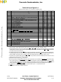
The SCIM consists of the following functional blocks:
• The system configuration and protection block controls configuration parameters
and provides bus and software watchdog monitors. In addition, it provides a peri-
odic interrupt generator to support execution of time-critical control routines.
• The system clock generates clock signals used by the SCIM, other IMB modules,
and external devices.
• The external bus interface handles the transfer of information between IMB mod-
ules and external address space.
• The chip-select block provides nine chip-select signals. Each chip-select signal
has an associated base register and option register that contain the programma-
ble characteristics of that chip select. Two additional chip selects allow external
emulation of on-chip SCIM I/O ports and ROM arrays. A data port, port C, is avail-
able for discrete output on pins not being used for their chip-select function or al-
ternate function as address or function code lines.
• The system test block incorporates hardware necessary for testing the MCU. Its
use in normal applications is not supported.
When the external data bus is fully expanded, two data ports, port E and port F, are
available for general-purpose input and output if not required for their alternate func-
tion. When the external data bus is partially expanded, port H is available in addition
to ports E and F. When the SCIM is configured for single-chip operation, six data ports
are available for general-purpose I/O: ports A, B, E, F, G, and H. A port data register,
data direction register, and pin assignment register are associated with each port.
The SCIM works with the CPU to support exception processing, including reset and
interrupt processing. Refer to
SECTION 6 INTERRUPTS
and
SECTION 8 RESET
AND SYSTEM INITIALIZATION
for additional information.
NOTE
Some SCIM-based MCUs have a reduced pin set due to pin limita-
tions. Some of the chip-select and data port pins described in this
manual may not be present on these MCUs. Refer to the user's man-
ual for the particular MCU for a list of the available pins on the device.
Refer to
SECTION 10 REDUCED PIN-COUNT SCIM
for a discus-
sion of SCIM operation with a reduced pin count.
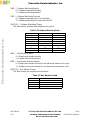
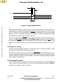
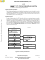
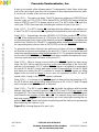
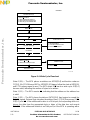
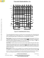
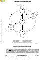
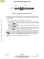
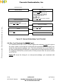
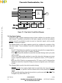
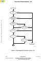
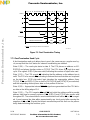
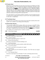
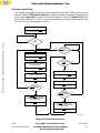
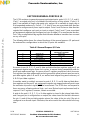
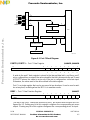
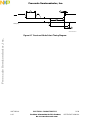
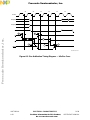
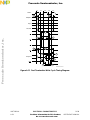
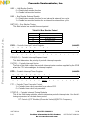
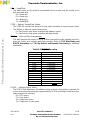
Figure 1-1
is a block diagram of the SCIM.
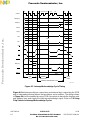
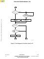
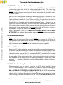
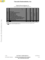
Figure 1-2
shows the input and output sig-
nals associated with each functional block of the SCIM. These signals are described
more fully in
SECTION 2 SIGNAL AND PIN DESCRIPTIONS
and in subsequent sec-
tions of the manual.
Frees
cale Semiconductor,
I
Freescale Semiconductor, Inc.
For More Information On This Product,
Go to: www.freescale.com
nc...

SCIM
INTRODUCTION
MOTOROLA
REFERENCE MANUAL 1-3
Figure 1-1 Single-Chip Integration Module Block Diagram
SCIM BLOCK
SYSTEM CONFIGURATION
AND PROTECTION
CLOCK SYNTHESIZER
CHIP SELECTS
EXTERNAL BUS INTERFACE
FACTORY TEST
CLKOUT
EXTAL
MODCLK
EXTERNAL BUS
RESET
TSC
FREEZE/QUOT
CHIP SELECTS
Frees
cale Semiconductor,
I
Freescale Semiconductor, Inc.
For More Information On This Product,
Go to: www.freescale.com
nc...

MOTOROLA
INTRODUCTION
SCIM
1-4 REFERENCE MANUAL
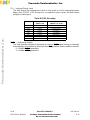
Figure 1-2 SCIM Input and Output Signals
IRQ[7:1]
ADDR[23:0]
CONTROL
PORT F PORT C
FC2
FC1
FC0
BG
BR
BGACK
MODCLK
ADDR[23:19]
CLOCK
EBI
CS[10:0]
BGACK/CSE
BG/CSM
BR/CS0
R/W
RESET
HALT
BERR
CLKOUT
XTAL
EXTAL
CHIP
SELECTS
CSBOOT
PA[7:0]/ADDR[18:11]
QUOT
TEST
FREEZE/QUOT
TSC
CONTROL
TSC
PC0/FC0/CS3
PC1/FC1/CS4
PC2/FC2/CS5
PC3/ADDR19/CS6
PC4/ADDR20/CS7
PC5/ADDR21/CS8
PC6/ADDR22/CS9
ECLK/ADDR23/CS10
PF7/IRQ7
PF6/IRQ6
PF5/IRQ5
PF4/IRQ4
PF3/IRQ3
PF2/IRQ2
PF1/IRQ1
PF0/MODCLK
CONTROL
PORT E
SIZ1 PE7/SIZ1
SIZ0 PE6/SIZ0
DSACK0 PE0/DSACK0
DSACK1 PE1/DSACK1
AVEC PE2/AVEC
PE3/RMC
AS PE5/AS
RMC
PE4/DS
XFC
V
DDSYN
CONTROL
DS
CONTROL
PORT A/B
PB[7:0]/ADDR[10:3]
ADDR[2:0]
DATA[15:0]
PG[7:0]/DATA[15:8]
CONTROL
PORT G/H
PH[7:0]/DATA[7:0]
ADDR[2:0]
SCIM PINOUT
FROM CPU
SCIM
Frees
cale Semiconductor,
I
Freescale Semiconductor, Inc.
For More Information On This Product,
Go to: www.freescale.com
nc...

SCIM
INTRODUCTION
MOTOROLA
REFERENCE MANUAL 1-5
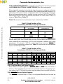
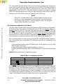
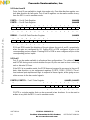
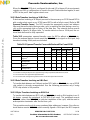
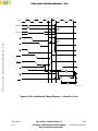
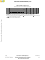
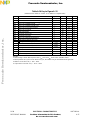
1.1 SCIM Address Map
Control registers for all the modules in the microcontroller are mapped into a 4-Kbyte
block. The state of the module mapping (MM) bit in the SCIM configuration register
(SCIMCR) determines where the control register block is located in the system mem-
ory map. When MM = 0, register addresses range from $7FF000 to $7FFFFF. When
MM = 1, register addresses range from $FFF000 to $FFFFFF.
CAUTION
On CPU16-based MCUs, ADDR[23:20] follow the logic state of
ADDR19 unless externally driven. If MM is cleared on these MCUs,
the SCIM maps IMB modules into an address space which is inac-
cessible to the CPU. Modules remain inaccessible until reset occurs.
The reset state of MM is one, but the bit can be written once. Initial-
ization software should make certain it remains set by writing a one
to it.
Table 1-1
is the SCIM address map. The column labeled “Access” indicates the priv-
ilege level at which the CPU must be operating to access the register. A designation
of “S” indicates that supervisor access is required; a designation of “S/U” indicates that
the register can be programmed to the desired privilege level. Refer to
3.1 Module
Configuration and Testing
for information on assigning privilege levels.
NOTE
CPU16-based MCUs do not support separate supervisor and user
privilege levels. The CPU16 always operates at the supervisor privi-
lege level.
Table 1-1
provides SCIM register addresses relative to the SCIM base address. In this
table, the four high-order nibbles of each address are listed as $####. Refer to the us-
er's manual for the specific MCU for the exact location of these registers. Remember
that the MSB is determined by the MM bit.
Frees
cale Semiconductor,
I
Freescale Semiconductor, Inc.
For More Information On This Product,
Go to: www.freescale.com
nc...

MOTOROLA
INTRODUCTION
SCIM
1-6 REFERENCE MANUAL
Table 1-1 SCIM Address Map
Access Address 15 8 7 0
S $####00 SCIM CONFIGURATION REGISTER (SCIMCR)
S $####02 MODULE TEST (SCIMTR)
S $####04 CLOCK SYNTHESIZER CONTROL (SYNCR)
S $####06 UNUSED RESET STATUS REGISTER (RSR)
S $####08 MODULE TEST E (SCIMTRE)
S/U $####0A PORT A DATA (PORTA) PORT B DATA (PORTB)
S/U $####0C PORT G DATA (PORTG) PORT H DATA (PORTH)
S/U $####0E PORT G DATA DIRECTION (DDRG) PORT H DATA DIRECTION (DDRH)
S/U $####10 UNUSED PORT E DATA (PORTE0)
S/U $####12 UNUSED PORT E DATA (PORTE1)
S/U $####14 PORT A/B DATA DIRECTION
(DDRAB)
PORT E DATA DIRECTION (DDRE)
S $####16 UNUSED PORT E PIN ASSIGNMENT (PEPAR)
S/U $####18 UNUSED PORT F DATA (PORTF0)
S/U $####1A UNUSED PORT F DATA (PORTF1)
S/U $####1C UNUSED PORT F DATA DIRECTION (DDRF)
S $####1E UNUSED PORT F PIN ASSIGNMENT (PFPAR)
S $####20 UNUSED SYSTEM PROTECTION CONTROL
(SYPCR)
S $####22 PERIODIC INTERRUPT CONTROL (PICR)
S $####24 PERIODIC INTERRUPT TIMING (PITR)
S $####26 UNUSED SOFTWARE SERVICE (SWSR)
S $####28 UNUSED PORT F EDGE DETECT FLAGS
(PORTFE)
S $####2A UNUSED PORT F EDGE DETECT INTER-
RUPT VECTOR (PFIVR)
S $####2C UNUSED PORT F EDGE DETECT INTER-
RUPT LEVEL (PFLVR)
S/U $####2E UNUSED
S $####30 TEST MODULE MASTER SHIFT A (TSTMSRA)
S $####32 TEST MODULE MASTER SHIFT B (TSTMSRB)
S $####34 TEST MODULE SHIFT COUNT A
(TSTSCA)
TEST MODULE SHIFT COUNT B
(TSTSCB)
S $####36 TEST MODULE REPETITION COUNTER (TSTRC)
S $####38 TEST MODULE CONTROL (CREG)
S/U $####3A TEST MODULE DISTRIBUTED REGISTER (DREG)
S/U $####3C UNUSED UNUSED
S/U $####3E UNUSED UNUSED
S/U $####40 UNUSED PORT C DATA (PORTC)
S/U $####42 UNUSED UNUSED
S $####44 CHIP-SELECT PIN ASSIGNMENT 0 (CSPAR0)
S $####46 CHIP-SELECT PIN ASSIGNMENT 1 (CSPAR1)
S $####48 CHIP-SELECT BASE ADDRESS BOOT (CSBARBT)
S $####4A CHIP-SELECT OPTION BOOT (CSORBT)
S $####4C CHIP-SELECT BASE 0 (CSBAR0)
S $####4E CHIP-SELECT OPTION 0 (CSOR0)
S $####50 UNUSED
S $####52 UNUSED
S $####54 UNUSED
Frees
cale Semiconductor,
I
Freescale Semiconductor, Inc.
For More Information On This Product,
Go to: www.freescale.com
nc...
Page is loading ...
Page is loading ...
Page is loading ...
Page is loading ...
Page is loading ...
Page is loading ...
Page is loading ...
Page is loading ...
Page is loading ...
Page is loading ...
Page is loading ...
Page is loading ...
Page is loading ...
Page is loading ...
Page is loading ...
Page is loading ...
Page is loading ...
Page is loading ...
Page is loading ...
Page is loading ...
Page is loading ...
Page is loading ...
Page is loading ...
Page is loading ...
Page is loading ...
Page is loading ...
Page is loading ...
Page is loading ...
Page is loading ...
Page is loading ...
Page is loading ...
Page is loading ...
Page is loading ...
Page is loading ...
Page is loading ...
Page is loading ...
Page is loading ...
Page is loading ...
Page is loading ...
Page is loading ...
Page is loading ...
Page is loading ...
Page is loading ...
Page is loading ...
Page is loading ...
Page is loading ...
Page is loading ...
Page is loading ...
Page is loading ...
Page is loading ...
Page is loading ...
Page is loading ...
Page is loading ...
Page is loading ...
Page is loading ...
Page is loading ...
Page is loading ...
Page is loading ...
Page is loading ...
Page is loading ...
Page is loading ...
Page is loading ...
Page is loading ...
Page is loading ...
Page is loading ...
Page is loading ...
Page is loading ...
Page is loading ...
Page is loading ...
Page is loading ...
Page is loading ...
Page is loading ...
Page is loading ...
Page is loading ...
Page is loading ...
Page is loading ...
Page is loading ...
Page is loading ...
Page is loading ...
Page is loading ...
Page is loading ...
Page is loading ...
Page is loading ...
Page is loading ...
Page is loading ...
Page is loading ...
Page is loading ...
Page is loading ...
Page is loading ...
Page is loading ...
Page is loading ...
Page is loading ...
Page is loading ...
Page is loading ...
Page is loading ...
Page is loading ...
Page is loading ...
Page is loading ...
Page is loading ...
Page is loading ...
Page is loading ...
Page is loading ...
Page is loading ...
Page is loading ...
Page is loading ...
Page is loading ...
Page is loading ...
Page is loading ...
Page is loading ...
Page is loading ...
Page is loading ...
Page is loading ...
Page is loading ...
Page is loading ...
Page is loading ...
Page is loading ...
Page is loading ...
Page is loading ...
Page is loading ...
Page is loading ...
Page is loading ...
Page is loading ...
Page is loading ...
Page is loading ...
Page is loading ...
Page is loading ...
Page is loading ...
Page is loading ...
Page is loading ...
Page is loading ...
Page is loading ...
Page is loading ...
Page is loading ...
Page is loading ...
Page is loading ...
Page is loading ...
Page is loading ...
Page is loading ...
Page is loading ...
Page is loading ...
Page is loading ...
Page is loading ...
Page is loading ...
Page is loading ...
Page is loading ...
Page is loading ...
Page is loading ...
Page is loading ...
Page is loading ...
Page is loading ...
Page is loading ...
Page is loading ...
Page is loading ...
Page is loading ...
Page is loading ...
Page is loading ...
Page is loading ...
Page is loading ...
Page is loading ...
Page is loading ...
Page is loading ...
Page is loading ...
Page is loading ...
Page is loading ...
Page is loading ...
Page is loading ...
Page is loading ...
Page is loading ...
Page is loading ...
Page is loading ...
Page is loading ...
Page is loading ...
Page is loading ...
Page is loading ...
Page is loading ...
Page is loading ...
Page is loading ...
Page is loading ...
Page is loading ...
Page is loading ...
Page is loading ...
Page is loading ...
Page is loading ...
Page is loading ...
Page is loading ...
Page is loading ...
Page is loading ...
Page is loading ...
Page is loading ...
Page is loading ...
Page is loading ...
Page is loading ...
Page is loading ...
Page is loading ...
Page is loading ...
Page is loading ...
Page is loading ...
Page is loading ...
Page is loading ...
Page is loading ...
Page is loading ...
Page is loading ...
Page is loading ...
Page is loading ...
Page is loading ...
Page is loading ...
Page is loading ...
Page is loading ...
-
 1
1
-
 2
2
-
 3
3
-
 4
4
-
 5
5
-
 6
6
-
 7
7
-
 8
8
-
 9
9
-
 10
10
-
 11
11
-
 12
12
-
 13
13
-
 14
14
-
 15
15
-
 16
16
-
 17
17
-
 18
18
-
 19
19
-
 20
20
-
 21
21
-
 22
22
-
 23
23
-
 24
24
-
 25
25
-
 26
26
-
 27
27
-
 28
28
-
 29
29
-
 30
30
-
 31
31
-
 32
32
-
 33
33
-
 34
34
-
 35
35
-
 36
36
-
 37
37
-
 38
38
-
 39
39
-
 40
40
-
 41
41
-
 42
42
-
 43
43
-
 44
44
-
 45
45
-
 46
46
-
 47
47
-
 48
48
-
 49
49
-
 50
50
-
 51
51
-
 52
52
-
 53
53
-
 54
54
-
 55
55
-
 56
56
-
 57
57
-
 58
58
-
 59
59
-
 60
60
-
 61
61
-
 62
62
-
 63
63
-
 64
64
-
 65
65
-
 66
66
-
 67
67
-
 68
68
-
 69
69
-
 70
70
-
 71
71
-
 72
72
-
 73
73
-
 74
74
-
 75
75
-
 76
76
-
 77
77
-
 78
78
-
 79
79
-
 80
80
-
 81
81
-
 82
82
-
 83
83
-
 84
84
-
 85
85
-
 86
86
-
 87
87
-
 88
88
-
 89
89
-
 90
90
-
 91
91
-
 92
92
-
 93
93
-
 94
94
-
 95
95
-
 96
96
-
 97
97
-
 98
98
-
 99
99
-
 100
100
-
 101
101
-
 102
102
-
 103
103
-
 104
104
-
 105
105
-
 106
106
-
 107
107
-
 108
108
-
 109
109
-
 110
110
-
 111
111
-
 112
112
-
 113
113
-
 114
114
-
 115
115
-
 116
116
-
 117
117
-
 118
118
-
 119
119
-
 120
120
-
 121
121
-
 122
122
-
 123
123
-
 124
124
-
 125
125
-
 126
126
-
 127
127
-
 128
128
-
 129
129
-
 130
130
-
 131
131
-
 132
132
-
 133
133
-
 134
134
-
 135
135
-
 136
136
-
 137
137
-
 138
138
-
 139
139
-
 140
140
-
 141
141
-
 142
142
-
 143
143
-
 144
144
-
 145
145
-
 146
146
-
 147
147
-
 148
148
-
 149
149
-
 150
150
-
 151
151
-
 152
152
-
 153
153
-
 154
154
-
 155
155
-
 156
156
-
 157
157
-
 158
158
-
 159
159
-
 160
160
-
 161
161
-
 162
162
-
 163
163
-
 164
164
-
 165
165
-
 166
166
-
 167
167
-
 168
168
-
 169
169
-
 170
170
-
 171
171
-
 172
172
-
 173
173
-
 174
174
-
 175
175
-
 176
176
-
 177
177
-
 178
178
-
 179
179
-
 180
180
-
 181
181
-
 182
182
-
 183
183
-
 184
184
-
 185
185
-
 186
186
-
 187
187
-
 188
188
-
 189
189
-
 190
190
-
 191
191
-
 192
192
-
 193
193
-
 194
194
-
 195
195
-
 196
196
-
 197
197
-
 198
198
-
 199
199
-
 200
200
-
 201
201
-
 202
202
-
 203
203
-
 204
204
-
 205
205
-
 206
206
-
 207
207
-
 208
208
-
 209
209
-
 210
210
-
 211
211
-
 212
212
-
 213
213
-
 214
214
-
 215
215
-
 216
216
-
 217
217
-
 218
218
-
 219
219
-
 220
220
-
 221
221
-
 222
222
-
 223
223
-
 224
224
-
 225
225
-
 226
226
-
 227
227
-
 228
228


Ask a question and I''ll find the answer in the document
Finding information in a document is now easier with AI
Related papers
Other documents
-
Motorola CPU32 Reference guide
-
Freescale Semiconductor MC68332 User manual
-
-
-
-
AVE Video Serial Synchronous ATM Interface VSSI-PRO User manual
-
Midmark Medical Lighting Installation guide
-
ADTRAN 1xN User manual
-
 MOBASE ELECTRONICS MBECFOB2402 User manual
-
