C
C
C
o
o
o
l
l
l
o
o
o
u
u
u
r
r
r
T
T
T
V
V
V
S
S
S
e
e
e
r
r
r
v
v
v
i
i
i
c
c
c
e
e
e
M
M
M
a
a
a
n
n
n
u
u
u
a
a
a
l
l
l

2
Model No: 21SHS3-CE.doc
Version 1.0
Group Model:
21SHS3
M
M
M
o
o
o
d
d
d
e
e
e
l
l
l
:
:
:
2
2
2
1
1
1
S
S
S
H
H
H
S
S
S
3
3
3
/
/
/
C
C
C
E
E
E
C
C
C
h
h
h
a
a
a
s
s
s
s
s
s
i
i
i
s
s
s
:
:
:
U
U
U
O
O
O
C
C
C
-
-
-
O
O
O
M
M
M
8
8
8
3
3
3
7
7
7
0
0
0

3
Model No: 21SHS3-CE.doc
Version 1.0
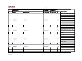
CONTENT
SAFETY NOTICE ................................................................................................................................... 4
GENERAL DESCRIPTION .................................................................................................................... 6
TECHNICAL SPECIFICATION ............................................................................................................. 7
GENERAL SPECIFICATION................................................................................................................. 8
HORIZONTAL AND VERTICAL CIRCUIT ......................................................................................... 9
CHASSIS BLOCK DIAGRAM ............................................................................................................. 10
FAULT FINDING TREES..................................................................................................................... 11
IC BLOCK DIAGRAM ......................................................................................................................... 18
FACTORY MENU
................................................................................................................................ 40
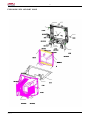
EXPLODED VIEW AND PART NAME .............................................................................................. 43
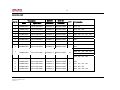
BOM LIST ............................................................................................................................................. 44
CIRCUIT DIAGRAM............................................................................................................................ 61

4
Model No: 21SHS3-CE.doc
Version 1.0
SAFETY NOTICE
WARNING: BEFORE EXAMINING AND
SERVICING THIS CHASSIS, READ
CAREFULLY THE FOLLOWING
SAFETY INSTRUCTIONS.
X-RAY RADIATION PRECAUTION
1. The primary source of X-RADIATION in television receiver is the picture tube. The picture tube
is specially constructed to limit X-RADIATION emissions. For continued X-RADIATION
protection, the replacement tube must be the same type as the original including suffix letter.
Excessive high voltage may produce potentially hazardous X-RADIATION. To avoid such
hazards, the high voltage must be maintained within specified limit. Refer to this service manual,
high voltage adjustment for specific high voltage limit. If high voltage exceeds specified limits,
take necessary corrective action. Carefully follow the instructions for +B1 volt power supply
adjustment, and high voltage check to maintain the high voltage within the specified limits.
2. The EHT must be checked every time the receiver is serviced to ensure that the CRT does not emit
X-ray radiation as result of excessive EHT voltage. The nominal EHT for this receiver is 22KV at
zero beam current (minimum brightness) operating at AC 220V. The maximum EHT voltage
permissible in any operating circumstances must not exceed 25KV. When checking the EHT, use
the High Voltage Check procedure in this manual using an accurate EHT voltmeter.
3. The only source of X-RAY radiation in this receiver is the CRT. To prevent X-ray radiation, you
should use the same type of CRT when replacing it.
4. Some components used in this receiver have safety-related characteristics preventing the CRT
from emitting X-ray radiation. For continued safety, replacement component should only be made
after referring the Product Safety notice below.
SAFETY PRECAUTION
1. The high voltage in the TV reaches to 22KV when the TV is in operation. Be more careful during
opening the back cover.
a) The high voltage existing in the TV is very dangerous. Refer servicing to qualified personnel
only.
b) Before removing the high voltage cap. Discharge the anode of the CRT and the chassis in
case of electric shock.
c) Wear a pair of goggles when handling the CRT to avoid broken pieces damaging your eyes.
d) Do not hold the CRT neck in case of causing damage to the CRT.
2. When the power cord needs replacing, use the same one as that provided by AKIRA factory.
3. Voltage exists between the hot and cold ground when TV is in operation. Install a separation
transformer during repairing or connecting to any tester for the sake of safety. The power of the
separation transformer should be beyond rated overall power.
4. When replacing a burnout fuse, use the one with the same specifications as the original.

5
Model No: 21SHS3-CE.doc
Version 1.0
5. When replacing old wire, wind new one round the shaft to weld. When replacing components with
safety in performance, use the same type as that specified by AKIRA and install it in the former
way.
6. Never place wire near high-temperature or high-voltage components.
7. An isolation transformer should be connected in the power line between the receiver and the AC
line when a service is performed on the primary of the converter transformer of the set.
8. Comply with all caution and safety-related notes provided on the cabinet back, inside the cabinet,
on the chassis or the picture tube.
9. When replacing a chassis in the cabinet, always be certain that all the protective devices are
installed properly, such as, control knobs, adjustment covers or shields, barriers, isolation resistor-
capacitor networks etc.. Before returning any television to the customer, the service technician
must be sure that it is completely safe to operate without danger of electrical shock.
PRODUCT SAFETY NOTICE
Product safety should be considered when a component replacement is made in any area of a receiver.
Components indicated by mark in the parts list and the schematic diagram designate components in
which safety can be of special significance. It is particularly recommended that only parts designated
on the parts list in this manual be used for component replacement designated by mark. No deviations
from resistance wattage or voltage ratings may be made for replacement items designated by mark.

6
Model No: 21SHS3-CE.doc
Version 1.0
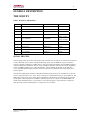
GENERAL DESCRIPTION
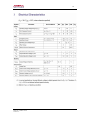
THE SURVEY
Table 1, the main IC and functions
Number Function IC Remark
1 Power supply KA5Q0765RT N611
2 CPU + SIGNAL PROCESSER OM 8370 /TDA9370 N301
3 Field driver STV9302A N401
4 Sound driver AN7522N N161
5 AV SWITCH TC4052BP
N801 (Video)
N161 (sound)
6 Memory AT24C08 N702
7 Photo-coupler PC817B N504
8 IR-receiver HS0038A2 U701
9 8V regulator L7808CV N503
10 5V regulator L7805CV N505
SIGNAL PROCESS
The TV signal enters into tuner (A201) from cable or antenna. Pin 10 and pin 11 of N301 are combined
to select the band. Pin 4 of N301 outputs PWM tuning signal. The 38.9MHz IF signal is coupled to
V308 (pre-amplify) and then to SAWF (Z301). After processed in the SAWF, the 38.9MHz signal gets
to pin 23 and pin 24 of OM8370. The IF circuit in OM8370 includes such unit as the AGC amplifying
circuit, 38.9MHz oscillator, PLL video demodulator, video amplifier, IF identify circuit and AFT
circuit. The demodulated signal (CVBS) comes from the pin 38 of OM8370, the sound signal comes
from the pin 44.
The internal CVBS signal needs norm identification then outputs from pin 38 of OM8370, via the trap
circuit (composed of the V351, Z351, Z354, V352 and so on) feeds back to the pin 40 of OM8370. The
RGB signal comes from pin51, Pin52, Pin53 of OM8370, and outputs to the CRT board. The internal
sound signal comes from pin 44 of OM8370 and then input to pin 1 and pin 12 of HEF4052BP. The
sound signals from RF and AV are selected in it. The selected signal is output from Pin 3 and pin13,
then input AN7522N (sound amplifier) or output from AV terminals.

7
Model No: 21SHS3-CE.doc
Version 1.0
TECHNICAL SPECIFICATION
Test Item Conditional TD171
AC Operating
Range
RF&AV signal input with sound loud speaker
(volume maximum) & Picture set in Dynamic
mode
140Vac ~ 240Vac
Philips or Mono-scope pattern signal with howling
sound Contrast & Brightness set in Maximum,
sound increase maximum
90Watts
Total Power
Consumption
Standby Mode 14 Watts
Brightness & contrast set in Maximum Min: 26.2KVdc
Typical Design value Average: 26.5KVdc
EHT
Brightness &contrast Minimum Max: 27.8KVdc
Anode Current Brightness &contrast Maximum I
ABL
≤ 1.2mA
Heater Voltage TV operate normally V
Heater
= 6.2Vac
B
+
Normal operating VB
+
= 112Vdc
Sound power
output
RF signal input broadcasting at
217.25MHz/BG/DK(1KHz)
Volume is maximum
V = 6.3Vrms
P = 5Watts X 2

8
Model No: 21SHS3-CE.doc
Version 1.0
GENERAL SPECIFICATION
14” 70W MAX
Power consumption
21” 90W MAX
Receive system DK/BG/I
Color system PAL/ SECAM/ NTSC
Vision intermediate frequency 38.9MHz
5.5 MHz(B/G)
Inter-carrier frequency
6.5MHz(D/K)
Chroma if frequency PAL 34.47/ 35.32MHz
Antenna type DIN TYPE 75 Ohm
VHF Low channel (VL) =48.25
to
147.25
MHz
VHF high channel (VH) =154.25
to
463.25
MHz
Channel receiving
UHF channel (U) =471.25
to
863.25
MHz
Tuning system VS tuning
AV IN/ OUT 2 AV STEREO IN + 1 AV STEREO OUT
Component IN 1 YUV-Component IN
VIDEO IN ----1.0 0.2V
p-p
75 Ohm
AUDIO IN ----0-2V (RMS)
VIDEO OUT ----1.0 0.2V
p-p
75 Ohm
AV IN/ OUT specification
AUDIO OUT ---- 0-2V (RMS)
OSD language
English, Russian, Turkish, French, Spanish,
Vietnamese, Indonesian, Arabian, Persian
Audio output power > 8W (1KHz, 0.5V INPUT, 10% THD
Safety authentication standard CB
LED indicator Power ON
Hand set type HS08
Hans set power supply Pin AAx2
Color picture tube 14” 21” 90 degree tube
Remote control distance 5m
Video/Audio (L/R) 2set input
YUV input
S-Video input
External input/output
Video/ Audio (L/R) 1 set output
I
2
C Bus Control
Auto Search
Off/On Timer
Teletext

9
Model No: 21SHS3-CE.doc
Version 1.0
HORIZONTAL AND VERTICAL CIRCUIT
Through Synchronous separating circuit, the video signal is divided into horizontal-Synchronizing
signal and Vertical-Synchronizing signal. The horizontal-Sync pulse coming from pin 33 is transferred
to the horizontal-drive transistor.
The cathode driving voltage 180V vertical drive voltage +15V and –15V are all generated from
FBT.
The vertical sawtooth waveform is generated on the pin 21 and 22, and then enters the vertical
amplifier STV9302A. STV9302A is a 7 pins vertical deflection circuit (2 Amperes) for DC-coupled
90° or 110° deflection systems with frame frequencies from 50 up to 120 Hz. one supply voltage for
the scanning and second voltage supply for the flyback are needed.
The vertical drive currents of OM8370 pins 21 and 22 are connected to input pins 1 and 7 of
STV9302A. The vertical scanning output is coming from pin 5 and feed back to pin 1 by R405. The
supply voltage is ±15V at pin 2 and pin 4. C406 is the pump capacitor.
POWER SUPPLY
The IC of KA5Q0765RT is adapted in this chassis; it is the product of Fairchild. It supplies four DC
voltages, one is the +B=110V, another is Hcc=26V, the third is 13V (the sound drive voltage), the
fourth is +16V. The +16V can generate the +8V, +5V and +3.3V by the special generators.

10
Model No: 21SHS3-CE.doc
Version 1.0
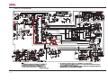
CHASSIS BLOCK DIAGRAM
HEAT
FOCUS
EHT
SCREEN
CRT
+300V
AUDIO AMPLIFIER
(N101) AN7522N
SP161
8Ω5W
SP162
8Ω5W
POWER SUPPLY
CIRCUIT
V1512
、、
V553 V1511
、
T
501
、
N504
Resistance
disturbance
C501
、 L502
AC150-260V
50/60Hz
Bridge
rectification
VD503-VD506
Filter C507
FBT(T402)
BSC25
110V
200V
24V
13V
16V
AV SWITH
N161
()
CD4052
AV SWITH
N801
()
CD4052
Video-out
Audio-out
()
L
Audio-out
()
R
Video-in1
Audio-in1
()
L
Audio-in1
()
R
Y
Cr
Cb
S-video
V-in2 A-in2
()
LA-in2
(
R
)
15
14
13
9
10
1
2 3 4 5
11
15
14
13
12
9
10
12
10
4
2
6
8
9
PHILIPS UOC
TDA9351/61/81
VIDEO
AMPLIFIER
V912
,
V913
V922
,
V923
V932
,
V933
FIELD OUTPUT
POWER AMP
。
N401
()
LA78040
HORIZONTAL
OUTPUT
V451
HORIZONTAL
DRIVE
V450
T450
HF TUNER
A101
IF PRE-AMP
V308
SAWF
Z301
KEY BOARD
REMOTE
RECEIVER
U701
MEMORY
N702
()
ST24C08
11
42
62
63
44
47
48
46
43
38 7
TV AUDIO OUT
SIF TRAPS
Z351,Z352,Z354
V351
V352
40
10
11
BAND2
BAND1
23
24
6
64
2
3
6
5
SCL
SDA
53
52
51
21
22
33
+15V
-15V
15V
R
L

11
Model No: 21SHS3-CE.doc
Version 1.0
FAULT FINDING TREES
A Three-None(no raster, no picture, no sound)
This failure is mainly caused by big-power circuit such as power supply, horizontal scanning, vertical scanning.
The detail checking and repairing steps are as follow.
0V
4.5-5.5V
YES
0V
>
1V
0.6V
300V
N
O
YES
0V
300V
0V
0V
115V
N
o variation
N
ormal
115V
0V
Others
24V
2V
8V
115V
LOW
N
O
variation
<
50V
Test the voltage of C528B
Cut off R458
T
T
T
e
e
e
s
s
s
t
t
t
o
o
o
t
t
t
h
h
h
e
e
e
r
r
r
v
v
v
o
o
o
l
l
l
t
t
t
a
a
a
g
g
g
e
e
e
s
s
s
u
u
u
c
c
c
h
h
h
a
a
a
s
s
s
1
1
1
8
8
8
8
8
8
V
V
V
,
,
,
2
2
2
4
4
4
V
V
V
,
,
,
a
a
a
n
n
n
d
d
d
1
1
1
2
2
2
V
V
V
VD525,VD1561,VR501,V542,
VD1517,V504,V1511
Check VD522,C528B
Recover R458, unplug
XS403 for a While,then
test the voltage of C528B
Check V451,T451,T450,
Deflection coil
Check L452,VD436,C461
Deflection coil
Voltage of C507
Check if V1513 collect-emitter
Was broken down
Check XR502,F501,power
Swich, AC cord and plug
Check the voltage
of V1513 collector
Check V1513,V1512,F501,XR502,VD503
Check T501
Test voltage of V1513 base
Check T501,VD1517,
C1515,C1517,V451,
VD522-VD529
C455,C456,T451
C467
Check if it get right
When cut off V504
Test the voltage of
N
301 pin1
CPU has sent the
Power-off signal
Check if V504
is broken down
Check V1513
Check R539,V1553,VD1561
N
504,V1511,V1512,R556
N
301 pin39voltage
N
301 pin33 voltage
Check N301,N401
V450 pin C voltage
Check VD543,C525,
]R454,C453,T450,
C455,V451
Check R452,V450
Check T451
Check V451 pin C voltage
Check T451,V451,R458
>
130V
Others
115V
0V

12
Model No: 21SHS3-CE.doc
Version 1.0
B Two-None (no picture, no sound)
The failure shows that the set does not display the picture but it has noise wave or blue background or OSD on the screen. This means that the circuits of power supply, horizontal scanning, vertical scanning
and video amplification are normal and they are not considered in the repairing. The failures are mainly in the small signal processing circuits.
Before checking these circuits, a kind of practical test method is introduced. It is called “Signal-input way ”. The detail is described as follow: We can use the resistance function of an analog multimeter,
connect the red pole (negative in ohm scope) on the circuit board ground, then touch softly the test point with another pole (black pole) in ohm scope meanwhile observe the reactivity on the output device.
Note : In the TV test, we mainly observe the noise wave on the CRT and listen to the noise voice liking as “Ka…..Ka” from the loudspeakers.
1. No picture
YES
N
o variatio
n
Out of the “ 0-33V ” range
0V
N
O
No picture
Check the “ +5V ” voltage on A101
Check RF signal input and adaptor
Check N703, A101
Check R301,R302,
N
301,A101
Check the “ VT ” voltage when auto searching
Check R707, C707, A101
The voltage between VL and BH vary from 0V to
5V or not when auto searching
Check R703,N703,C703A
The voltage on the C703
Check the voltage on the C705
Check ,V701,N301, R701, R701A
,R704,R705,C701,C705,C706
Check if A101 has input signal
0V
YES
In the “ 0-33V ” range
5V
<
33V
=
33V
0-33V

13
Model No: 21SHS3-CE.doc
Version 1.0
YES
0V
>
3.8V
<
2V
Exam the voltage of “ AGC ” on A101 without antenna
Check R317, R318, R316,C307,A101,N301
Test the voltage on pin 14, 54, 56of N301
N
O
YES
YES
N
O
≥2V
YES
N
O
0V
YES
Check,L331, C333, L752,C753A, L751, C751
Test the voltage on pin 51, 52, 53, 50 of N301
Check N505, N301
Check N503, N301,C532, R565,C524,
,VD561,V542
Observe if there is snow-noise-wave disturbance on the CRT via using “Signal-input way ” by touching pin 23 and pin 24 of N301
Observe if there is snow-noise-wave disturbance on the CRT via using “Signal-input way ”by touching pin 17 of N301
Check R331,C336,C337
Observe if snow-noise-wave disturbance on the CRT via using “ signal-input way ”by touching pin 40 of N301
Test if there is the sync signal on the pin 39 of N301
Check V351,V352,L351,Z351,C364
Check C323,A101,N301
Observe if there is snow-noise-wave disturbance on the CRT via using “ Signal-input way ” by touching pin 38 of N301
Check if voltage on pin 31 of N301 is 1.7V
Check C361,C362,L361,N301
Observe if these is snow-noise-wave disturbance on the CRT via using “ Signal-input way ” by touching pin 51,52,53 of N301
Check R381,R382,R383,V912,V922,V932,N301
8V
5V
N
O
N
O
N
O

14
Model No: 21SHS3-CE.doc
Version 1.0
5. No sound
In this kind of failure, first of all we should observe if there is the picture on the CRT. It proves the small signal circuit to work correctly with the picture on the CRT and we only check the sound signal
processing and sound amplification circuit. The repairing method(B1) may be referred without picture. The detail checking and repairing steps are as follow.
Note:
Before repairing, assure that the volume is on and the state of set is in “TV” .
<
5V
YES
YES
N
O
N
O
<
8V
YES
N
O
YES
YES
YES
N
O
Hear if there is the voice liking “Ka…Ka ” in the loudspeaker via using “ Signal-input way ” by touching pin 7 of N301
Check C367,R369,V395,N301
Hear if there is the voice liking “Ka…Ka ” in the loudspeaker via using “ Signal-input way ” by touching pin 3 of N121
Hear if there is the voice liking “Ka…Ka ” in the loudspeaker via using “ Signal-input way ” by touching pin 44 of N301
Check R733, C732, N301
Check R126,N505, N121
The voltage on pin 9,10of N121
Check 8V-power supply
Hear if there is the voice liking “Ka…Ka ” in the loudspeaker via using “ Signal-input way ” by touching pin 2,10 of N701
Check VD521,R165,C522,T501,N161
The voltage on pin 16 of N121
Hear if there is the voice liking “Ka…Ka ” in the loudspeaker via using “ Signal-input way ” by touching pin 13 of N121
Check R157,C157,N161
Hear if there is the voice liking “Ka…Ka ” in the loudspeaker via using “ Signal-input way ” by touching pin 6,8of N161
The voltage on pin 1 of N701
Check R153,C153,R154,C154,N121
Check C157,C153, N101
Check SP161, SP162, N161
N
O
8V
8V
12.5V
N
O

15
Model No: 21SHS3-CE.doc
Version 1.0
C Only horizontal line in the middle of the screen:
If vertical deflection circuit does not work, this kind of failure will happen. In deflection yoke, there only has horizontal sweeping , the electron beam in the CRT only moves in the horizontal orientation , so
form this failure.
(While checking horizontal and vertical deflection circuit’ s failure , we have better to use an oscilloscope.)
Abnormal
N
ormal
N
ormal
Abnormal
24V
0V
Abnormal
N
ormal
The waveform on the pin 21,22 of N301
Measuring the waveform on the deflection yoke
Check C401,C402,R401,R402,N301
The voltage on pin 2 of N401
Check VD470, R470,VD401,N401
Check N402
Measuring the waveform on pin 1 of N401
Check R405, C408, N401, N301
Measuring the waveform on pin 5 of N401
Check R407,C408,R406,XS403, deflection yoke
Abnormal
The deflection yoke on the CRT

16
Model No: 21SHS3-CE.doc
Version 1.0
D Only vertical line in the middle of the screen
This is a dangerous failure. It probable causes flashover and smoking inside the set. Don’ t let your TV work for a long time as this failure appears. Because the electron beam can not move in the horizontal
orientation, the failure should be in the horizontal deflection circuit. We mainly check the open-circuit fault in horizontal deflection circuit. The detail checking and repairing steps are as follow:
E UOC does not work
In television, remote-control system is similar with the computer system. In theory , it can work if it holds two conditions as follow:
1) The power supply: In general, it is 5V, the error is not above 10% and the disturbance pulse is as small as possible.
2) The clock pulse: In TDA93XX circuit, the clock pulse is generated by pin58 / pin59 of N301 and 12M crystal oscillator.
Television’ s remote-control system also needs reset circuit that can preset the values in internal register. The circuit around pin57
of N204 is called auto-reset circuit. If UOC detects errors in resetting, it will come to the state of programme protected.
YES
YES
N
O
Vertical line
Repair CRT
The horizontal yoke is opened or not
Whether “ XS403” is opened
Check if there is bad solder between XS403, and the main board
Check L452, VD436, C467,C455,especial in inductive components and connector
N
O

17
Model No: 21SHS3-CE.doc
Version 1.0
The detail checking and repairing steps are as follow:
F No OSD (On Screen Display)
This failure is usually cause by the circuit of character generated and located. Most of reasons are that the horizontal and vertical flyback pulse signals do not come to UOC.
We can judge this failure by measuring the wave of the character in an oscilloscope.
The detail checking and repairing steps are as follow:
3V
<
3.3V
=14V
<
3.3V
YES
=3.3V
N
O
<
3.3V 3.3V
N
301 does not work
The voltage on the pin 56 of N301
Observe if there is sine wave on the pin 58 or pin 59
of N301 with an oscilloscope
Check the voltage on the positive pole of C548
N
O
YES
3.3V
3.3V
Check alternant voltage on secondary coil of N505,
Check X761, N301
Check R561,VD564
Check the voltage on the pin 54 of N301
Check T501, VD522,R565
Check N301
Check the voltage on the emitter of VD564
Check the voltage on the positive pole of VD522
Check VD522, T501
Check R565,R546,N505
Check L752,L753
YES
N
O
Check FBT T451
No OSD
Check the wave on the pin 7 of FBT
Check C482, R485, VD483, R487, N301

18
Model No: 21SHS3-CE.doc
Version 1.0
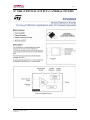
IC BLOCK DIAGRAM
Fig 1: OM8370 Illustration

19
Model No: 21SHS3-CE.doc
Version 1.0
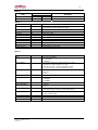
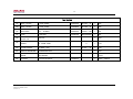
MAIN CHIP INSTRUCTION
Pin 1 Standby control, “1” is on, “0” is off.
Pin 2 SCL
Pin 3 SDA
Pin 4 Tuning PWM output
Pin 5 Auto AV control SW, connected with the SCART 8
th
pin. Input. The rising edge or
the falling edge operates.
Pin 6 Key board input.
Pin 7 Volume
Pin 8 Mute control, “1” is mute, “0” is off.
Pin 9, Pin 12,
Pin 18, Pin 30,
Pin 35, Pin 41,
Pin 55
GND
Pin 10 BAND 1 control output.
Pin 11 BAND 2
Pin 13 SECAM PLL, connected with a capacitance (no use in this type).
Pin 14 +8V power source supply
Pin 15 Using a capacitor of 220n in series to GND. This pin decouples the internal digital
supply voltage of the video process and minimizes the disturbance to the sensitive
analogue parts.
Pin 16 Phase-2 control loop, this pin requires a capacitor at 2.2nF © in series to GND.
Pin 17 Phase-1 control loop filter connected to pin 17 is suitable for various signal
conditions like strong /weak and VCR signal. This is achieved by switching of the
loop filter time constant by changing the Phase-1 output current.
Pin 18 GND
Pin 19 Bandgap decoupling, the bandgap circuit provides a very stable and temperature
independent reference voltage. This reference voltage (4.0V) ensures optimal
performance of the analogue video processor part of the OM8370 and is used in
almost all functional circuit blocks.
Pin 20 East-west pillow signal output.
Pin 21, Pin 22 Vertical drive output.
Pin 23, Pin 24 IF input.
Pin 25 Reference current/ This pin requires a resistor to ground. The optimal reference
current is 100mA which is determined by this resistor. The 100mA reference
current should not be changed because the geometry processor is optimized for this
current. Furthermore the output current of vertical drive and EW are proportional to
this current.
Pin 26 Vertical sawtooth. This pin requires a capacitor to ground of 100nF.
Pin 27 AGC output. This output is used to control (reduce) the tuner gain for strong RF
signals.
Pin 28 Audio de-emphasis.
Pin 29 Sound decoupling. This pin requires a capacitor connected to ground. The pin acts
as a low pass filter needed for the DC feedback loop.
Pin 30 GND
Pin 31 Sound loop filter.
Pin 32 AVL filter
Pin 33 Horizontal drive signal output, needs a resistor in series to +8V.
Pin 34 Sandcastle output /flyback input.
Pin 35 External audio input, this pin should be grounded in this chassis.

20
Model No: 21SHS3-CE.doc
Version 1.0
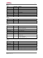
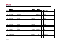
Pin 36 EHT tracking /over voltage protection. If something is wrong, the anode high
voltage rise the heater voltage will rise too. When the rising voltage arrive some
limit, the V406 works, the voltage of pin 36 will exceed 3.9V. The OM8370 will
stop working.
Pin 37 PLL loop filter.
Pin 38 CVBS output. Monitor or RF videos can be selected.
Pin 39 +8V supply source
Pin 40 CVBS input
Pin 42 Y signal input
Pin 43 C signal input
Pin 44 Main audio output. This pin is connected to the TDA9859.
Pin 45 RGB signal input blanking.
Pin 46, Pin 47,
Pin 48
RGB signal input.
Pin 49 ABL. It means been current limiter input. R410 is the control resistor.
Pin 50 Black current input from the CRT board.
Pin 51, Pin 52,
Pin 53
RGB drive signal output to the CRT board.
Pin 54 +3.3V
Pin 55 GND
Pin 56 +3.3V
Pin 57, Pin 58,
Pin 59
12MHz crystal
Pin 60 Reset. NC in this chassis
Pin 61 +3.3V
Pin 62 NC
Pin 63 This pin is connected to the HEF4094. Functions expending.
Pin 64 IR signal input.
Page is loading ...
Page is loading ...
Page is loading ...
Page is loading ...
Page is loading ...
Page is loading ...
Page is loading ...
Page is loading ...
Page is loading ...
Page is loading ...
Page is loading ...
Page is loading ...
Page is loading ...
Page is loading ...
Page is loading ...
Page is loading ...
Page is loading ...
Page is loading ...
Page is loading ...
Page is loading ...
Page is loading ...
Page is loading ...
Page is loading ...
Page is loading ...
Page is loading ...
Page is loading ...
Page is loading ...
Page is loading ...
Page is loading ...
Page is loading ...
Page is loading ...
Page is loading ...
Page is loading ...
Page is loading ...
Page is loading ...
Page is loading ...
Page is loading ...
Page is loading ...
Page is loading ...
Page is loading ...
Page is loading ...
-
 1
1
-
 2
2
-
 3
3
-
 4
4
-
 5
5
-
 6
6
-
 7
7
-
 8
8
-
 9
9
-
 10
10
-
 11
11
-
 12
12
-
 13
13
-
 14
14
-
 15
15
-
 16
16
-
 17
17
-
 18
18
-
 19
19
-
 20
20
-
 21
21
-
 22
22
-
 23
23
-
 24
24
-
 25
25
-
 26
26
-
 27
27
-
 28
28
-
 29
29
-
 30
30
-
 31
31
-
 32
32
-
 33
33
-
 34
34
-
 35
35
-
 36
36
-
 37
37
-
 38
38
-
 39
39
-
 40
40
-
 41
41
-
 42
42
-
 43
43
-
 44
44
-
 45
45
-
 46
46
-
 47
47
-
 48
48
-
 49
49
-
 50
50
-
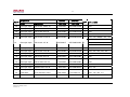 51
51
-
 52
52
-
 53
53
-
 54
54
-
 55
55
-
 56
56
-
 57
57
-
 58
58
-
 59
59
-
 60
60
-
 61
61


Ask a question and I''ll find the answer in the document
Finding information in a document is now easier with AI