
ELECTRONIC DEVICES DIVISION
PWM STEP-UP DC/DC CONVERTER
RH5RH××1A/××2B/××3B SERIES
APPLICATION MANUAL
NO.EA-023-9803

NOTICE
1. The products and the product specifications described in this application manual are subject to change or dis-
continuation of production without notice for reasons such as improvement. Therefore, before deciding to use
the products, please refer to Ricoh sales representatives for the latest information thereon.
2. This application manual may not be copied or otherwise reproduced in whole or in part without prior written con-
sent of Ricoh.
3. Please be sure to take any necessary formalities under relevant laws or regulations before exporting or other-
wise taking out of your country the products or the technical information described herein.
4. The technical information described in this application manual shows typical characteristics of and example
application circuits for the products. The release of such information is not to be construed as a warranty of or a
grant of license under Ricoh's or any third party's intellectual property rights or any other rights.
5. The products listed in this document are intended and designed for use as general electronic components in
standard applications (office equipment, computer equipment, measuring instruments, consumer electronic
products, amusement equipment etc.). Those customers intending to use a product in an application requiring
extreme quality and reliability, for example, in a highly specific application where the failure or misoperation of
the product could result in human injury or death (aircraft, spacevehicle, nuclear reactor control system, traffic
control system, automotive and transportation equipment, combustion equipment, safety devices, life support
system etc.) should first contact us.
6. We are making our continuous effort to improve the quality and reliability of our products, but semiconductor
products are likely to fail with certain probability. In order prevent any injury to persons or damages to property
resulting from such failure, customers should be careful enough to incorporate safety measures in their design,
such as redundancy feature, fire-containment feature and fail-safe feature. We do not assume any liability or
responsibility for any loss or damage arising from misuse or inappropriate use of the products.
7. Anti-radiation design is not implemented in the products described in this application manual.
8. Please contact Ricoh sales representatives should you have any questions or comments concerning the prod-
ucts or the technical information.
June 1995

OUTLINE
......................................................................................................
1
FEATURES
....................................................................................................
1
APPLICATIONS
.............................................................................................
1
BLOCK DIAGRAM
.........................................................................................
2
SELECTION GUIDE
.......................................................................................
2
PIN CONFIGURATION
...................................................................................
3
PIN DESCRIPTION
........................................................................................
3
ABSOLUTE MAXIMUM RATINGS
...................................................................
4
ELECTRICAL CHARACTERITICS
...................................................................
5
OPERATION OF STEP-UP DC/DC CONVERTER
...........................................
10
TYPICAL CHARACTERISTICS
......................................................................
13
1) Output Voltage vs. Output Current
.......................................................................
13
2) Efficiency vs. Output Current
.............................................................................
14
3) Supply Current (No Load) vs. Input Voltage
..............................................................
15
4) Output Current vs. Ripple Voltage
........................................................................
15
5) Start-up/Hold-on Voltage vs. Output Current (Topt=25˚C)
...............................................
16
6) Output Voltage vs. Temperature
.........................................................................
17
7) Start-up Voltage vs. Temperature
........................................................................
18
8) Hold-on Voltage vs. Temperature
........................................................................
18
9) Supply Current 1 vs. Temperature
.......................................................................
18
10) Supply Current 2 vs. Temperature
.......................................................................
18
11) Lx Switching Current vs. Temperature
...................................................................
18
12) Lx Leakage Current vs. Temperature
....................................................................
18
13) Oscillator Frequency vs. Temperature
....................................................................
19
14) Oscillator Duty Cycle vs. Temperature
...................................................................
19
15) Vlx Voltage Limit vs. Temperature
........................................................................
20
16) EXT “H” Output Current vs. Temperature
................................................................
20
17) EXT “L” Output Current vs. Temperature
.................................................................
20
18) Load Transient Response
................................................................................
21
19) Distribution of Output Voltage
............................................................................
22
20) Distribution of Oscillator Frequency
......................................................................
22
RH5RH SERIES
APPLICATION MANUAL
CONTENTS

TYPICAL APPLICATIONS
............................................................................
23
• RH5RH××1A
.................................................................................................
23
• RH5RH××2B
..................................................................................................
23
• RH5RH××3B
..................................................................................................
24
• CE pin Drive Circuit
............................................................................................
22
APPLICATION CIRCUITS
.............................................................................
26
• 12V Step-up Circuit
............................................................................................
26
• Step-down Circuit
..............................................................................................
26
• Step-up/Step-down Circuit with Flyback
.......................................................................
27
PACKAGE DIMENSIONS
..............................................................................
28
TAPING SPECIFICATIONS
...........................................................................
28

PWM STEP-UP DC/DC CONVERTER
1
RH5RH
××
1A/
××
2B/
××
3B SERIES
OUTLINE
The RH5RH××1A/××2B/××3B Series are PWM Step-up DC/DC converter ICs by CMOS process.
The RH5RH
××1A IC consists of an oscillator, a PWM control circuit, a driver transistor (Lx switch), a refer-
ence voltage unit, an error amplifier, a phase compensation circuit, resistors for voltage detection, a soft-start cir-
cuit, and an Lx switch protection circuit. A low ripple, high efficiency step-up DC/DC converter can be constructed
of this RH5RH
××1A IC with only three external components, that is, an inductor, a diode and a capacitor.
These RH5RH
××1A/××2B/××3B ICs can achieve ultra-low supply current (no load) –TYP. 15µA –by a new-
ly developed PWM control circuit, equivalent to the low supply current of a VFM (chopper) Step-up DC/DC con-
verter.
Furthermore, these ICs can hold down the supply current to TYP. 2µA by stopping the operation of the oscil-
lator when the input voltage > (the output voltage set value + the dropout voltage by the diode and the inductor).
These RH5RH
××1A/××2B/××3B Series ICs are recommendable to the user who desires a low ripple PWM
DC/DC converter, but cannot adopt a conventional PWM DC/DC converter because of its too large supply current.
The RH5RH
××2B/××3B Series ICs use the same chip as that employed in the RH5RH××1A IC and are pro-
vided with a drive pin (EXT) for an external transistor. Because of the use of the drive pin (EXT), an external
transistor with a low saturation voltage can be used so that a large current can be caused to flow through the
inductor and accordingly a large output current can be obtained. Therefore, these RH5RH
××2B/××3B Series ICs
are recommendable to the user who need a current as large as several tens mA to several hundreds mA.
The RH5RH
××3B IC also includes an internal chip enable circuit so that it is possible to set the standby sup-
ply current at MAX. 0.5µA.
These RH5RH
××1A/××2B/××3B ICs are suitable for use with battery-powered instruments with low noise
and low supply current.
•
Small Number of External Components
..........
Only an inductor, a diode and a capacitor (RH5RH
××
1A)
•
Low Supply Current
...........................................
TYP. 15µA (RH5RH301A)
•
Low Ripple and Low Noise
•
Low Start-up Voltage (when the output current is 1mA)
..................
MAX. 0.9V
•
High Output Voltage Accuracy
..........................
±2.5%
•
High Efficiency
...................................................
TYP. 85%
•
Low Temperature-Drift Coefficient of Output Voltage
......................
TYP. ±50 ppm/˚C
•
Soft-Start
.............................................................
MIN. 500µs
•
Small Packages
...................................................
SOT-89 (RH5RH
××
1A, RH5RH
××
2B),
SOT-89-5 (RH5RH
××
3B)
FEATURES
APPLICATIONS
•
Power source for battery-powered equipment.
•
Power source for cameras, camcorders, VCRs, PDAs, electronic data banks,and hand-held communication
equipment.
•
Power source for instruments which require low noise and low supply current, such as hand-held audio equip-
ment.
•
Power source for appliances which require higher cell voltage than that of batteries used in the appliances.

2
RH5RH
×××× – ×× ← Part Number
↑ ↑ ↑
a b c
SELECTION GUIDE
In RH5RH Series, the output voltage, the driver, and the taping type for the ICs can be selected at the user's
request. The selection can be made by designating the part number as shown below :
For example, the product with Output Voltage 5.0V, the External Driver (the Oscillator Frequency 100kHz)
and Taping Type T1, is designated by Part Number RH5RH502B-T1.
Code Description
Setting Output Voltage (VOUT):
a
Stepwise setting with a step of 0.1V in the range of 2.7V to 7.5V is possible.
Designation of Driver:
1A: Internal Lx Tr. Driver (Oscillator Frequency 50kHz)
b 2B: External Tr. Driver (Oscillator Frequency 100kHz)
3B: Internal Tr./External Tr. (selectively available) (Oscillator Frequency 100kHz, with chip
enable function)
Designation of Taping Type :
c
Ex. SOT-89
:
T1, T2
SOT-89-5
:
T1, T2
(refer to Taping Specifications)
“T1” is prescribed as a standard.
RH5RH
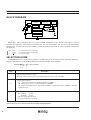
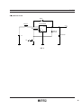
BLOCK DIAGRAM
Lx
Vss
EXT
LxSW
CE
Error Amp.
OUT
V
LX limiter
Buffer
PWM control
OSC
Chip Enable
Slow start
Phase Comp.
Vref
+
–
Error Amp. (Error Amplifier) has a DC gain of 80dB, and Phase Comp. (Phase Compensation Circuit)
provides the frequency characteristics including the 1st pole (fp=0.25Hz) and the zero point (fz=2.5kHz).
Furthermore, another zero point (fz=1.0kHz) is also obtained by the resistors and a capacitor connected to
the OUT pin.
(Note) Lx Pin
............
only for RH5RH××1A and RH5RH××3B
EXT Pin
.........
only for RH5RH
××2B and RH5RH××3B
CE Pin
...........
only for RH5RH
××3B
}
}
}

3
•
SOT-89-5
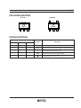
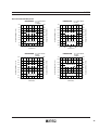
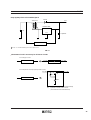
PIN CONFIGURATION
•
SOT-89
PIN DESCRIPTION
Pin No.
××1B ××2B ××3B
1 1 5
2 2 2
3 — 4
— 3 3
— — 1
1 2
3
(mark side)
1 2
3
(mark side)
5
4
RH5RH
Symbol Description
VSS Ground Pin
OUT Step-up Output Pin, Power Supply (for device itself)
Lx Switching Pin (Nch Open Drain)
EXT External Tr. Drive Pin (CMOS Output)
CE Chip Enable Pin (Active Low)

4
RH5RH
ABSOLUTE MAXIMUM RATINGS
Symbol Item
VOUT Output Pin Voltage
VLX Lx Pin Voltage
VEXT EXT Pin Voltage
VCE CE Pin Voltage
ILX Lx Pin Output Current
IEXT EXT Pin Current
PD Power Dissipation
Topt Operating Temperature Range
Tstg Storage Temperature Range
Tsolder Lead Temperature(Soldering)
Rating Unit Note
+12 V
+12 V Note1
– 0.3 to VOUT+0.3 V Note2
–0.3 to VOUT+0.3 V Note3
250 mA Note1
±50 mA Note2
500 mW
–30 to +80 ˚C
–55 to +125 ˚C
260˚C,10s
(Note 1) Applicable to RH5RH××1A and RH5RH××3B. (Note 2) Applicable to RH5RH××2B and RH5RH××3B.
(Note 3) Applicable to RH5RH
××3B.
Vss=0V
Absolute Maximum ratings are threshold limit values that must not be exceeded even for an instant under any
conditions. Moreover, such values for any two items must not be reached simultaneously. Operation above
these absolute maximum ratings may cause degradation or permanent damage to the device. These are stress
ratings only and do not necessarily imply functional operation below these limits.
ABSOLUTE MAXIMUM RATINGS

5
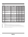
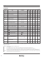
ELECTRICAL CHARACTERISTICS
• RH5RH301A
Symbol Item
VOUT Output Voltage
VIN Input Voltage
Vstart Start-up Voltage
Vhold Hold-on Voltage
I
DD1 Supply Current 1
IDD2 Supply Current 2
ILX Lx Switching Current
ILXleak Lx Leakage Current
fosc Oscillator Frequency
Maxdty
Oscillator Maximum Duty
Cycle
η
Efficiency
tstart Soft-Start Time
VLXlim VLX Voltage Limit
Conditions MIN. TYP. MAX. Unit Note
2.925 3.000 3.075 V
8 V
IOUT=1mA,V
IN : 0→2V 0.8 0.9 V
IOUT=1mA,VIN : 2→0V 0.7 V
To be measured at OUT Pin
(excluding Switching Current)
15 25 µA
To be measured at OUT Pin
(excluding Switching Current) 2 5 µA
VIN=3.5V
VLX=0.4V 60 mA
VLX=6V,VIN=3.5V 0.5 µA
40 50 60 kHz
on (VLX “L” ) side 70 80 90 %
70 85 %
Time required for the rising
0.5 2.0 ms Note1
of VOUT up to 3V.
Lx Switch ON 0.65 0.8 1.0 V Note2
VOUT=3.0V
RH5RH
Unless otherwise provided, VIN=1.8V, VSS=0V, IOUT=10mA, Topt=25˚C, and use External Circuit of Typical
Application (FIG. 1).
(Note 1) Soft-Start Circuit is operated in the following sequence :
(1) V
IN is applied.
(2) The voltage (Vref) of the reference voltage unit is maintained at 0V for about 200µs after the application of V
IN.
(3) The output of Error Amp. is raised to “H” level during the maintenance of the voltage (Vref) of the reference voltage unit.
(4) After the rise of Vref, the output of Internal Error Amp. is gradually decreased to an appropriate value by the function of Internal Phase
Compensation Circuit, and the Output Voltage is gradually increased in accordance with the gradual decrease of the output of Internal Error
Amp.
(Note 2) I
LX is gradually increased after Lx Switch is turned ON. In accordance with the increase of ILX, VLX is also increased. When VLX reaches VLXlim,
Lx Switch is turned OFF by an Lx Switch Protection Circuit.

6
RH5RH
• RH5RH501A
VOUT=5.0V
Unless otherwise provided, VIN=3V, Vss=0V, IOUT=10mA, Topt=25˚C, and use External Circuit of Typical
Application (FIG. 1).
(Note 1) Soft-Start Circuit is operated in the following sequence :
(1) V
IN is applied.
(2) The voltage (Vref) of the reference voltage unit is maintained at 0V for about 200µs after the application of V
IN.
(3) The output of Error Amp. is raised to “H” level during the maintenance of the voltage (Vref) of the reference voltage unit.
(4) After the rise of Vref, the output of Internal Error Amp. is gradually decreased to an appropriate value by the function of Internal Phase
Compensation Circuit, and the Output Voltage is gradually increased in accordance with the gradual decrease of the output of Internal Error
Amp.
(Note 2) I
LX is gradually increased after Lx Switch is turned ON. In accordance with the increase of ILX, VLX is also increased. When VLX reaches VLXlim,
Lx Switch is turned OFF by an Lx Switch Protection Circuit.
Symbol Item
VOUT Output Voltage
VIN Input Voltage
Vstart Start-up Voltage
Vhold Hold-on Voltage
I
DD
1 Supply Current 1
IDD2 Supply Current 2
ILX Lx Switching Current
ILXleak Lx Leakage Current
fosc Oscillator Frequency
Maxdty
Oscillator Maximum Duty
Cycle
η
Efficiency
tstart Soft-Start Time
VLXlim VLX Voltage Limit
Conditions MIN. TYP. MAX. Unit Note
4.875 5.000 5.125 V
8 V
Iout=1mA,Vin:0→2V 0.8 0.9 V
Iout=1mA,Vin:2→0V 0.7 V
To be measured at OUT Pin
(excluding Switching Current)
30 45 µA
To be measured at OUT Pin
(excluding Switching Current) 2 5 µA
VIN=5.5V
VLX=0.4V 80 mA
VLX=6V,VIN=5.5V 0.5 µA
40 50 60 kHz
on (VLX “L” ) side 70 80 90 %
70 85 %
Time required for the rising
0.5
2.0
ms Note1
of VOUT up to 5V.
Lx Switch ON 0.65 0.8 1.0 V Note2

7
RH5RH
• RH5RH302B
Symbol Item
VOUT Output Voltage
VIN Input Voltage
Vstart Oscillator Start-up Voltage
IDD
1
Supply Current 1
IDD
2
Supply Current 2
IEXTH EXT “H” Output Current
IEXTL EXT “L” Output Current
fosc Oscillator Frequency
Maxdty
Oscillator Maximum Duty
Cycle
tstart Soft-Start Time
Conditions MIN. TYP. MAX. Unit Note
2.925 3.000 3.075 V
8 V
EXT no load,VOUT :0→2V 0.7 0.8 V
EXT no load,VOUT=2.88V 30 50 µA
EXT no load,VOUT=3.5V 2 5 µA
VEXT=V
OUT–0.4V –1.5 mA
VEXT=0.4V 1.5 mA
80 100 120 kHz
VEXT “H” side
70 80 90
%
Time required for the rising
0.5
2.0
ms Note1
of V
OUT up to 3V
VOUT=3.0V
Unless otherwise provided, VIN=1.8V, Vss=0V, IOUT=10mA, Topt=25˚C, and use External Circuit of Typical
Application (FIG. 2).
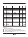
• RH5RH502B
VOUT=5.0V
Unless otherwise provided, VIN=3V, Vss=0V, IOUT=10mA, Topt=25˚C and use External Circuit of Typical
Application (FIG. 2).
(Note 1) refer to page 5 (Note 1)
Symbol Item
VOUT Output Voltage
VIN Input Voltage
Vstart Oscillator Start-up Voltage
IDD
1
Supply Current 1
IDD
2
Supply Current 2
IEXTH EXT “H” Output Current
IEXTL EXT “L” Output Current
fosc Oscillator Frequency
Maxdty
Oscillator Maximum Duty
Cycle
t
start Soft-Start Time
Conditions MIN. TYP. MAX. Unit Note
4.875 5.000 5.125 V
8 V
EXT no load,VOUT :0→2V 0.7 0.8 V
EXT no load,VOUT=4.8V 60 90 µA
EXT no load,VOUT=5.5V 2 5 µA
VEXT=VOUT–0.4V –2 mA
VEXT=0.4V 2 mA
80 100 120 kHz
VEXT “H” side
70 80 90 %
Time required for the rising
0.5 2.0 ms Note1
of V
OUT up to 5V

8
• RH5RH303B
Symbol Item
V
OUT Output Voltage
VIN Input Voltage
Vstart Start-up Voltage
Vhold Hold-on Voltage
η
Efficiency
IDD1 Supply Current 1
IDD2 Supply Current 2
ILX Lx Switching Current
ILXleak Lx Leakage Current
IEXTH EXT “H” Output Current
IEXTL EXT “L” Output Current
VCEH1 CE “H” Level 1
VCEL1 CE “L” Level 1
VCEH2 CE “H” Level 2
VCEL2 CE “L” Level 2
ICEH CE “H” Input Current
ICEL CE “L” Input Current
fosc Oscillator Frequency
Maxdty
Oscillator Maximum Duty
Cycle
tstart Soft-Start Time
VLXlim VLX Voltage Limit
Conditions MIN. TYP. MAX. Unit Note
2.925 3.000 3.075 V
8 V
IOUT=1mA,V
IN : 0
→
2V 0.8 0.9 V
IOUT=1mA,VIN : 2
→
0V 0.7 V
70 85 %
To be measured at OUT pin 30 50 µA
To be measured at OUT pin
2 5 µA
VIN=3.5V
VLX=0.4V 60 mA
VLX=6V,VIN=3.5V 0.5 µA
VEXT=VOUT–0.4V –1.5 mA
VEXT=0.4V 1.5 mA
VOUT≥1.5V
VOUT–0.4
V
VOUT≥1.5V 0.4 V
0.8V≤VOUT<1.5V
VOUT–0.1
V
0.8V≤VOUT<1.5V 0.1 V
CE=3V 0.5 µA
CE=0V –0.5 µA
80 100 120 kHz
on (V
LX “L” )side 70 80 90 %
Time required for the rising
0.5 2.0 ms Note1
of VOUT up to 3V.
Lx Switch ON 0.65 0.8 1.0 V Note2
VOUT=3.0V
Unless otherwise provided, VIN=1.8V, VSS=0V, IOUT=10mA, Topt=25˚C, and use External Circuit of Typical
Application (FIG. 3).
(Note 1) Soft-Start Circuit is operated in the following sequence :
(1) V
IN is applied.
(2) The voltage (Vref) of the reference voltage unit is maintained at 0V for about 200µs after the application of V
IN.
(3) The output of Error Amp. is raised to “H” level during the maintenance of the voltage (Vref) of the reference voltage unit.
(4) After the rise of Vref, the output of Internal Error Amp. is gradually decreased to an appropriate value by the function of Internal Phase Com
pensation Circuit, and the Output Voltage is gradually increased in accordance with the gradual decrease of the output of Internal Error Amp.
(Note 2) I
LX is gradually increased after Lx Switch is turned ON. In accordance with the increase of ILX, VLX is also increased. When VLX reaches VLXlim,
Lx Switch is turned OFF by an Lx Switch Protection Circuit.
RH5RH

9
• RH5RH503B
VOUT=5.0V
RH5RH
Unless otherwise provided, VIN=3V, VSS=0V, IOUT=10mA, Topt=25˚C, and use External Circuit of Typical
Application (FIG. 3).
(Note 1) Soft-Start Circuit is operated in the following sequence :
(1) V
IN is applied.
(2) The voltage (Vref) of the reference voltage unit is maintained at 0V for about 200µs after the application of V
IN.
(3) The output of Error Amp. is raised to “H” level during the maintenance of the voltage (Vref) of the reference voltage unit.
(4) After the rise of Vref, the output of Internal Error Amp. is gradually decreased to an appropriate value by the function of Internal Phase Com
pensation Circuit, and the Output Voltage is gradually increased in accordance with the gradual decrease of the output of Internal Error Amp.
(Note 2) I
LX is gradually increased after Lx Switch is turned ON. In accordance with the increase of ILX, VLX is also increased. When VLX reaches VLXlim,
Lx Switch is turned OFF by an Lx Switch Protection Circuit.
Symbol Item
VOUT Output Voltage
VIN Input Voltage
Vstart Start-up Voltage
Vhold Hold-on Voltage
η
Efficiency
IDD1 Supply Current 1
IDD2 Supply Current 2
ILX Lx Switching Current
ILXleak Lx Leakage Current
IEXTH EXT “H” Output Current
IEXTL EXT “L” Output Current
VCEH1 CE “H” Level 1
VCEL1 CE “L” Level 1
VCEH2 CE “H” Level 2
VCEL2 CE “L” Level 2
ICEH CE “H” Input Current
ICEL CE “L” Input Current
fosc Oscillator Frequency
Maxdty
Oscillator Maximum Duty
Cycle
tstart Soft-Start Time
VLXlim VLX Voltage Limit
Conditions MIN. TYP. MAX. Unit Note
4.875 5.000 5.125 V
8 V
IOUT=1mA,VIN : 0
→
2V 0.8 0.9 V
IOUT=1mA,VIN : 2
→
0V 0.7 V
70 85 %
To be measured at OUT pin 60 90 µA
To be measured at OUT pin
2 5 µA
VIN=5.5V
V
LX=0.4V 80 mA
VLX=6V,VIN=5.5V 0.5 µA
VEXT=VOUT–0.4V –2.0 mA
VEXT=0.4V 2.0 mA
VOUT≥1.5V
VOUT–0.4
V
VOUT≥1.5V 0.4 V
0.8V≤VOUT<1.5V
VOUT–0.1
V
0.8V≤VOUT<1.5V 0.1 V
CE=5V 0.5 µA
CE=0V –0.5 µA
80 100 120 kHz
on (V
LX “L” )side 70 80 90 %
Time required for the rising
0.5 2.0 ms Note1
of VOUT up to 5V.
Lx Switch ON 0.65 0.8 1.0 V Note2

10
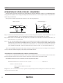
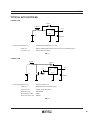
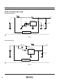
OPERATION OF STEP-UP DC/DC CONVERTER
Step-up DC/DC Converter charges energy in the inductor when Lx Transistor (LxTr) is on, and discharges the
energy with the addition of the energy from Input Power Source thereto, so that a higher output voltage than the
input voltage is obtained.
The operation will be explained with reference to the following diagrams :
< Current through L >< Basic Circuits >
RH5RH
i2
L
SD
I
OUT
VOUT
CLLx Tr
i1
V
IN
IL
ILmin
ILmax
topen
t
ton
toff
T=1/fosc
Step 1 : LxTr is turned ON and current IL (= i1 ) flows, so that energy is charged in L. At this moment, IL(=i1 ) is
increased from ILmin (= 0) to reach ILmax in proportion to the on-time period (ton) of LxTr.
Step 2 : When LxTr is turned OFF, Schottky diode (SD) is turned ON in order that L maintains IL at ILmax, so
that current IL (= i2) is released.
Step 3 : IL (=i2) is gradually decreased, and in the case of discontinuous mode, IL reaches ILmin (=0) after a time
period of topen, so that SD is turned OFF. However, in the case of a continuous mode which will be mentioned
later,the time period (toff) runs out before IL reaches ILmin (=0), so that LxTr is turned ON in the next
cycle, and SD is turned OFF. In this case, ILmin does not reach zero, and IL (=i1) increases from ILmin (> 0).
In the case of PWM control system, the output voltage is maintained constant by controlling the on-time peri-
od (ton), with the oscillator frequency (fosc) being maintained constant.
•
Discontinuous Conduction Mode and Continuous Conduction Mode
In the above two diagrams, the maximum value (ILmax) and the minimum value (ILmin) of the current which
flows through the inductor are the same as those when LxTr is ON and also when LxTr is OFF.
The difference between ILmax and ILmin, which is represented by ∆I, is :
∆I=ILmax–ILmin=V
IN · ton/L=(VOUT–VIN) · topen/L
.........................................
Equation 1
wherein T=1/fosc=ton+toff
duty (%)=ton/T · 100=ton · fosc · 100
topen≤toff
In Equation 1, V
IN · ton/L and (VOUT–VIN) · topen/L are respectively show the change in the current at ON, and the
change in the current at OFF.

11
RH5RH
When the output current (IOUT) is relatively small, topen<toff as illustrated in the above diagram. In this case,
the energy charged in the inductor during the time period of ton is discharged in its entirely during the time peri-
od of toff, so that ILmin becomes zero (ILmin=0). When I
OUT is gradually increased, topen eventually becomes
equal to toff (topen=toff), and when I
OUT is further increased. ILmin becomes larger than zero (ILmin>0). The
former mode is referred to as the discontinuous mode and the latter mode is referred to as the continuous mode.
In the continuous mode, when Equation 1 is solved for ton and the solution is tonc,
tonc =T · (1–V
IN/VOUT)
................................................................................................
Equation 2
When ton<tonc, the mode is the discontinuous mode, and when ton=tonc, the mode is the continuous mode.
•
Output Current in Discontinuous Mode
In the discontinuous mode, when LxTr is on, the energy P
ON charged in the inductor is provided by Equation 3
as follows :
P
ON=∫
0
ton
VIN · IL (t) dt =∫
0
ton
(VIN
2
· t/L) dt
=V
IN
2
· ton
2
/(2 · L)
.................................................................................................
Equation 3
In the case of the step-up DC/DC converter, the energy is also supplied from the input power source at the time
of OFF.
Thus, P
OFF=∫
0
topen
VIN · IL (t) dt =∫
0
topen
((VOUT–VIN) · t/L)dt
=V
IN · (VOUT–VIN) · topen
2
/(2 · L)
Here, topen=V
IN · ton/(VOUT–VIN) from Equation 1, and when this is substituted into the above equation.
=V
IN
3
· ton
2
/(2 · L · (V
OUT–VIN)
..........................................................................
Equation 4
Input power is (P
ON+POFF)/T. When this is converted in its entirely to the output.
P
IN=(PON+POFF)/T=VOUT · IOUT=POUT
.....................................................................
Equation 5
Equation 6 can be obtained as follows by solving Equation 5 for I
OUT by substituting Equations 3 and 4 into
Equation 5 :
I
OUT=VIN
2
· ton
2
/(2 · L · T · (VOUT–VIN))
.....................................................................
Equation 6
The peak current which flows through L · LxTr · SD is
ILmax=V
IN · ton/L
......................................................................................................
Equation 7

12
RH5RH
Therefore it is necessary that the setting of the input/output conditions and the selection of peripheral compo-
nents should be made with ILmax taken into consideration.
•
Output Current in Continuous Conduction Mode
When the operation enters into the continuous conduction mode by increasing the I
OUT, ILmin becomes equal
to Iconst (> 0), and this current always flows through the inductor. Therefore, V
IN · Iconst is added to PIN in
Equation 5.
Thus, P
IN=VIN · Iconst+(PON+POFF)/T=VOUT · IOUT=POUT
When the above Equation is solved for IOUT,
I
OUT=VIN
2
· tonc
2
/(2 · L · T · (VOUT–VIN))+VIN · Iconst/VOUT
............................................
Equation 8
The peak current which flows through L · LxTr · SD is
ILmax=V
IN · ton/L+Iconst
...................................................................................................
Equation 9
From Equations 6 and 9, the larger the value of L, the smaller the load current at which the operation enters
into the continuous mode, and the smaller the difference between ILmax and ILmin, and the smaller the value of
ILmax.
Therefore, when the load current is the same, the larger the value of L, the easier the selection of peripheral
components with a small allowable current becomes, and the smaller the ripple of the peripheral components can
be made. In this case, however, it must be noted from Equation 6 that I
OUT becomes small when the allowable cur-
rent of the inductor is small or when V
IN is so small that the operation cannot enter into the continuous mode.
The above explanation is directed to the calculation in an ideal case where there is no energy loss caused by the
resistance in the external components and LxSW. In an actual case, the maximum output current will be 50
to 80% of the above calculated maximum output current. In particular, care must be taken because V
IN is
decreased in an amount corresponding to the voltage drop caused by LxSW when IL is large or V
IN is low.
Furthermore, it is required that with respect to V
OUT, Vf of the diode (about 0.3V in the case of a Schottky type
diode) be taken into consideration.
HINTS

13
RH5RH
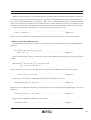
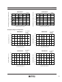
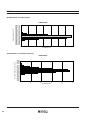
TYPICAL CHARACTERISTICS
1) Output Voltage vs. Output Current
RH5RH301A
L=120µH
V
IN=1.0V
1.5V
2.0V
0 20
40
60
3.1
3.0
2.9
2.8
2.7
2.6
2.5
Output Current I
OUT(mA)
Output Voltage VOUT(V)
L=270µH
1.5V
3.1
3.0
2.9
2.8
2.7
2.6
2.5
Output Current I
OUT(mA)
Output Voltage VOUT(V)
0
10 20 30
40
50 60
VIN=1.0V
2.0V
RH5RH501A
L=120µH
V
IN=
1.0V
Output Current I
OUT(mA)
Output Voltage VOUT(V)
3.0V
4.0V
0 50 100 150
4.0
4.2
4.4
4.6
4.8
5.0
5.2
2.0V
RH5RH302B
L=28µH
Output Current I
OUT(mA)
Output Voltage VOUT(V)
2.5V2.0V
1.5V
0 200 400 600
2.8
2.9
3.0
3.1
VIN=0.9V
RH5RH301A
RH5RH501A
L=270µH
V
IN=1.0V
Output Current I
OUT(mA)
Output Voltage VOUT(V)
2.0V
3.0V
4.0V
0
50 100 150
4.0
4.2
4.4
4.6
4.8
5.0
5.2
RH5RH502B
L=28µH
V
IN=1.5V
Output Current I
OUT(mA)
Output Voltage VOUT(V)
2.0V
3.0V
4.0V
0 500 1000
4.4
4.6
4.8
5.0
5.2

14
RH5RH
2) Efficiency vs. Output Current
RH5RH301A
L=120µH
V
IN=1.0V
1.5V
2.0V
0 10
20
30
90
80
70
60
50
40
Output Current I
OUT(mA)
Efficiency η (%)
L=270µH
1.5V
2.0V
0 10
20
30 40
90
100
80
70
60
50
40
Output Current I
OUT(mA)
Efficiency η (%)
VIN=1.0V
RH5RH501A
L=120µH
V
IN=1.0V
3.0V
4.0V
0 50
100
150
90
100
80
70
60
50
40
Output Current I
OUT(mA)
Efficiency η (%)
2.0V
RH5RH302B
L=28µH
V
IN=0.9V
2.0V
2.5V
0
200
400
600
80
100
60
40
20
0
Output Current I
OUT(mA)
Efficiency η (%)
1.5V
RH5RH301A
RH5RH501A
L=270µH
V
IN=
1.0V
3.0V
4.0V
2.0V
0 50
100
150
90
100
80
70
60
50
40
Output Current I
OUT(mA)
Efficiency η (%)
RH5RH502B
L=28µH
V
IN=1.5V
3.0V
4.0V
2.0V
0
500
1000
80
100
60
40
20
0
Output Current I
OUT(mA)
Efficiency η (%)

15
RH5RH
3) Supply Curret (No Load) vs. Input Voltage
4) Output Current vs.Ripple Voltage
RH5RH301A
L=120µH
1.0 1.2
1.4
1.6 1.8 2.0
50
60
70
40
30
20
10
0
Input Voltage V
IN(V)
Supply Current IIN (µA)
L=270µH
1.0 1.2
1.4
1.6 1.8 2.0
50
60
70
40
30
20
10
0
Input Voltage V
IN(V)
Supply Current IIN (µA)
RH5RH501A
L=120µH
1 2
3
4
200
150
100
50
0
Input Voltage V
IN(V)
Supply Current IIN (µA)
RH5RH301A
L=120µH
1
5
10
20 30 40
50
60
70
80
90 100
50
60
70
80
40
30
20
10
0
Output Current I
OUT(mA)
Ripple Voltage Vr (mV p-p)
VIN=0.9V
2.0V
3.0V
RH5RH301A
RH5RH501A
L=270µH
1 2
3
4
200
150
100
50
0
Input Voltage V
IN(V)
Supply Current IIN (µA)
RH5RH501A
L=120µH
1
5
10
20 30 40
50 60 70 80 90 100
50
60
70
80
90
100
40
30
20
10
0
Output Current I
OUT(mA)
Ripple Voltage Vr (mV p-p)
4.0V
3.0V
2.0V
VIN=0.9V

16
5) Start-up/Hold-on Voltage vs. Output Current (Topt=25˚C)
RH5RH
RH5RH301A
L=270µH
1
10
20 30
40 50 60 70 80
50
60
70
40
30
20
10
0
Output Current I
OUT(mA)
Ripple Voltage Vr (mV p-p)
2.0V
3.0V
VIN=0.9V
L=270µH
1
10
90
20 30 40 50
60 70 80
50
60
70
80
40
30
20
10
0
Output Current I
OUT(mA)
Ripple Voltage Vr (mV p-p)
2.0V
3.0V
4.0V
VIN=0.9V
RH5RH302B
L=28µH
1
50
100 150 200
50
60
70
40
30
20
10
0
Output Current I
OUT(mA)
Ripple Voltage Vr (mV p-p)
VIN=0.9V
2.0V
3.0V
RH5RH301A
L=120µH
0
10
20
30
1.0
1.2
1.4
0.8
0.6
0.4
0.2
0
Output Current I
OUT(mA)
Start-up/Hold-on Voltage Vstart/Vhold (V)
Vstart
Vhold
RH5RH501A
RH5RH502B
L=28µH
1
50
100 150
250
200
100
120
80
60
40
20
0
Output Current I
OUT(mA)
Ripple Voltage Vr (mV p-p)
VIN=0.9V
2.0V
3.0V
4.0V
RH5RH501A
L=120µH
0
10
20
30
1.0
1.2
1.4
1.6
0.8
0.6
0.4
0.2
0
Output Current I
OUT(mA)
Start-up/Hold-on Voltage Vstart/Vhold (V)
Vstart
Vhold
Page is loading ...
Page is loading ...
Page is loading ...
Page is loading ...
Page is loading ...
Page is loading ...
Page is loading ...
Page is loading ...
Page is loading ...
Page is loading ...
Page is loading ...
Page is loading ...
Page is loading ...
Page is loading ...
-
 1
1
-
 2
2
-
 3
3
-
 4
4
-
 5
5
-
 6
6
-
 7
7
-
 8
8
-
 9
9
-
 10
10
-
 11
11
-
 12
12
-
 13
13
-
 14
14
-
 15
15
-
 16
16
-
 17
17
-
 18
18
-
 19
19
-
 20
20
-
 21
21
-
 22
22
-
 23
23
-
 24
24
-
 25
25
-
 26
26
-
 27
27
-
 28
28
-
 29
29
-
 30
30
-
 31
31
-
 32
32
-
 33
33
-
 34
34


Ricoh RH5RH13B User manual
- Type
- User manual
- This manual is also suitable for
Ask a question and I''ll find the answer in the document
Finding information in a document is now easier with AI
Related papers
Other documents
-
Sanyo Battery Charger CR17450E-R User manual
-
-
-
Microchip Technology TC7660SEOA User manual
-
Sanyo ML414 Lithium User manual
-
Microchip Technology MCP1630V User manual
-
Airflow iCONstant HT Operating instructions
-
Carl Valentin ILX + Wipe-on applicators WMX Operating instructions
-
-