Page is loading ...

All Rights Reserved.
Attention please!
The information herein is given to describe certain components and shall not be considered
as a guarantee of characteristics. Terms of delivery and rights to technical change reserved.
We hereby disclaim any and all warranties, including but not limited to warranties of non-
infringement, regarding circuits, descriptions and charts stated herein.
Warnings
Under no circumstances may Infineon Technologies products of the brand AENEON
("Aeneon Product(s)") be used in any applications, devices or systems that are safety critical
or serve the purpose of supporting, maintaining, sustaining or protecting human life (such
applications, devices and systems collectively referred to as "Critical Systems"), if
1. A failure of the AENEON Products can reasonable be expected to –directly or indirectly–
a. Have a detrimental effect on such Critical Systems in terms of reliability, effectiveness
or safety; or
b. Cause the failure of such Critical Systems; or
2. A failure or malfunction of such Critical Systems can reasonably be expected to
–directly or indirectly–
a. Endanger the health or the life of the user of such Critical Systems or any other
person; or
b. Otherwise cause material damages (including but not limited to damages or serious
injury to life or property, whether tangible or intangible).
AENEON Data Sheet Revision Rev. 1.01, 2005-10
An Infineon Technologies Brand Doc. # 11162004-23IK-Z783
Simply advanced
Unbuffered Memory Module
Data Sheet
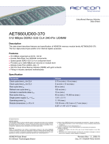
AET760UD00-370
1 GByte DDR2–533 CL4 240-Pin UDIMM
Description
This data sheet describes features and specification of AENEON memory module family AET760UD00-370.
The four digit product type postfix is for internal logistic purposes.
Features
1 GByte organized as 128 M × 64 bit
Double Data Rate Two SDRAM components
Speed grade DDR2–533 CL4 on component level
Provides up to 4264 MByte per second on module level
Module Code PC2–4200U–444–11
240-Pin Dual Inline Memory Module (DIMM) with gold contacts
Fitting in industry standard motherboards
Specification
Parameter Values
Clock cycle time t
CK
for CL4 3.75 ns (min.) / 8 ns (max.)
Clock cycle time t
CK
for CL3 5 ns (min.) / 8 ns (max.)
Row cycle time t
RC
60 ns (min.)
Refresh row cycle time t
RFC
127.5 ns (min.)
Activate to read/write delay t
RCD
15 ns (min.)
Row active time t
RAS
45 ns (min.) / 70.000 ns (max.)
Single power supply V
DD
= V
DDQ
1.8 V ± 0.1 V
Operating power I
DD0
2.3 W (max.)
Module dimensions L x W x H 133.35 mm x 30.0 mm x 4.0 mm (max.)
5.25" x 1.18" x 0.16" (max.)
/

