
FCC Information and Copyright
This equipment has been tested and found to comply with the limits of
a Class B digital device, pursuant to Part 15 of the FCC Rules. These
limits are designed to provide reasonable protection against harmful
interference in a residential installation. This equipment generates, uses
and can radiate radio frequency energy and, if not installed and used in
accordance with the instructions, may cause harmful interference to
radio communications. There is no guarantee that interference will not
occur in a particular installation.
The vendor makes no representations or warranties with respect to the
contents here of and specially disclaims any implied
warranties of
merchantability or fitness for any purpose. Further the vendor reserves
the right to revise this publication and to make changes to the contents
here of without obligation to notify any party beforehand.
Duplication of this publication, in part or in whole, is not allowed
without first obtaining the vendor’s approval in writing.
The content of this user’s manual is subject to be changed without
notice and we will not be responsible for any mistakes found in this
user’s manual. All the brand and product names are trademarks of their
respective companies.

Table of Contents
i
English .......................................................................................................1
1. Feature Introduction........................................................................... 1
1-1. U8598 Features (for V3.0) .......................................................................1
1-2. Package Contents.......................................................................................... 2
2. Mainboard Configuration................................................................... 3
2-1. Layout of U8598............................................................................................. 3
2-2. Component Index.......................................................................................... 4
3. CPU Configuration................................................................................ 5
3-1. CPU Socket 478 Configuration Steps:............................................... 5
3-2. CPU Fan Header: JCFAN1 .........................................................................7
3-3. System Fan Header: JSFAN1..................................................................7
4. Jumpers, Headers & Connectors.................................................... 8
4-1. Front Panel Connector: JPANEL1.......................................................... 9
4-2. ATX 20-pin Power Connector: JATXPWR1 ....................................11
4-3. ATX 12V Power Connector: JATXPWR2..........................................11
4-4. Hard Disk Connectors: IDE1/IDE2/IDE3 .......................................12
4-5. Floppy Disk Connector: FDD1 ..............................................................12
4-6. Wake On LAN Header: JWOL1.............................................................12
4-7. Clear CMOS Jumper: JCMOS1 .............................................................13
4-8. Front USB Header: JUSB3......................................................................13
4-9. Front USB Header: JUSB2......................................................................14
4-10. DDR DIMM Voltage: JDIMMVOLT (Optional) ............................14
4-11. AUX Power Connector: JAUXPWR1 ................................................14
4-12. Front 1394 Header: J1394A1(Optional)......................................14
4-13. Front 1394 Header: J1394B1(Optional)......................................15
4-14. Front 1394 Header: J1394C1(Optional)......................................15
4-15. Aux Audio in Connector: JAUX1 (Optional) ...............................15

Table of Contents
ii
4-16. Serial ATA Connector: JSATA1/ JSATA2 (Optional)..............15
5. RAM Module Configuration ............................................................. 16
5-1. DDR SDRAM....................................................................................................16
5-2. DIMM Module Configuration..................................................................17
6. Peripheral Port Features.................................................................. 18
6-1. PS/2 Mouse / Keyboard Connector: JKBMS1..............................18
6-2. USB & LAN Port Connectors: JUSBLAN1........................................19
6-3. Serial and Parallel Interface Ports......................................................21
6-4. Game (Joystick/MIDI) Port Connector: JGAME1.......................23
6-5. Audio Port Connectors: JSPKR1/JLIN1/JMIC1 ............................23
6-6. Audio Subsystem .........................................................................................25
Français ...................................................................................................27
1. U8598 Particularités (pour V3.0) : ................................................27
2. Dessin d’U8598 .............................................................................................29
Serial ATA Chip - FastTrak 376 ............................................................30
Step 1: Installing the Hard Drives................................................................30
Step 2: Auto Setup FastBuild™ Configuration Utility ........................31
Step 3: Installing Software Drivers..............................................................35
Step 4: Install PAM Utility..................................................................................40
Using FastBuild™ Configuration Utility.......................................................45

Mainboard Features
1
English
1. Feature Introduction
1-1. U8598 Features (for V3.0)
CPU
- Provides Socket-478.
- Supports the Intel Pentium 4 processor up to 3.06GHz.
- Running at 400/533MHz Front Side Bus.
Chipset
- North Bridge: VIA VT 8754(P4X400).
- South Bridge: VT8235.
Main Memory
- Supports up to 3 Double-Sided DDR devices.
- Supports 200/266/333MHz DDR devices.
- The largest memory capacity is 12GB.
Slots
- Five 32-bit PCI bus master slots.
- One CNR slot.
- One AGP slot.
On Board IDE
- Supports four IDE disk drives.
- Supports PIO Mode 4, Master Mode and Ultra DMA 33/66/100/133
Bus Master Mode.
1394 Chip (Optional)
- Support 3 ports (via external bracket) with transfer rate up to 400
Mbps.
Serial ATA (Optional)
- Built in 2 channels SATA PHY, which satisfy SATA 1.0 specification
and can transfer data with 1.5GHz speed.
- Additional one parallel ATA interface which satisfy ATA 133
specification.

Mainboard Features
2
Auto Negotiation
- Dual Speed: 10/100Mbps.
- Full/Half Duplex.
On Board AC’97 Sound Codec
- Compliant with AC’97 specification.
- Support 6-CH speaker mode.
On Board Peripherals
- Supports 360K, 720K, 1.2MB, 1.44MB and 2.88MB floppy disk
drivers.
- Supports 2 serial ports.
- Supports 1 multi-mode parallel port. (SPP/EPP/ECP mode)
- Supports PS/2 mouse and PS/2 keyboard.
- Supports 2 back USB2.0 ports and 4 front USB2.0 ports.
BIOS
- AWARD legal Bios.
- Supports APM1.2.
- Supports ACPI.
- Supports USB Function.
Operating System
- Offers the highest performance for MS-DOS, Windows 2000,
Windows Me, Windows XP, SCO UNIX etc.
Dimensions
- Micro ATX Form Factor: 24.5cm X 30.5cm (W X L)
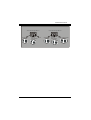
1-2. Package Contents
1.HDD Cable.
2.FDD Cable.
3.Flash Memory Writer for BIOS Update.
4.USB Cable (Optional).
5.Rear I/O Panel for ATX Case (Optional).
6.Fully Setup Driver CD.
7.IEEE1394 Cable (Optional).
8.Serial ATA Cable (Optional).

Mainboard Features
3
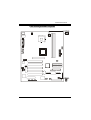
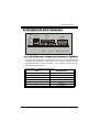
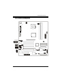
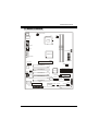
2. Mainboard Configuration
2-1. Layout of U8598
CPU
PCI1
PCI2
AGP SLOT
PCI SLOT
PCI SLOT
PCI SLOT
DIMM1
DIMM2
DIMM3
Socket 478
CPU1
JATXPWR1
VT8754
VT8235
JSFAN1
1
JPANEL1
12
2324
JKBMS1
Mouse &
KB
JUSBLAN1
USB & LAN
JCOM1
JPRNT1
JATXPWR2
JCOM2
JCDIN1
1
1
1
JTAD1
JCDIN2
BIOS
Winbond
W83697HF
PCI4
PCI SLOT
PCI SLOT
CNR SLOT
PCI5
CNR1
JDIMMVOLT
1
27
PRIMARY IDE CONN.
SECONDARY IDE CONN.
Parallel Port
JAUX1
1
8
PCI3
JAUXPWR1
Sp-Out
Line-InMic-In
Game Port
JGAME1
2
9
10
1
2
9
10
1
2
9
10
1
J1394A1
J1394B1
J1394C1
JWOL1
1
FLOPPY DISK CONN.
JUSB2
2
9
10
1
JUSB3
2
91
10
1394
CHIP
IDE3
BAT1
JCMOS1
1
Serials
ATA
Controller
JSATA2JSATA1
Codec
JAUDIO1
1
2
13
14
17
2
3
4
5
6
17
2
3
4
5
6

Mainboard Features
4
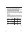
2-2. Component Index
Codec

Mainboard Features
5
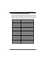
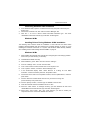
3. CPU Configuration
3-1. CPU Socket 478 Configuration Steps:
1. Pull the lever sideways away from the socket then raise the lever
up to a 90-degree angle.
2. Locate Pin A in the socket and look for the white dot or cut edge in
the CPU. Match Pin A with the white dot/cut edge then insert the
CPU.
3. Press the lever down. Then Put the fan on the CPU and buckle it
and put the fan’s power port into the JCFAN1, then to complete the
installation.
CPU Fan
CPU

Mainboard Features
6
CPU Configuration Layout
Codec

Mainboard Features
7
3-2. CPU Fan Header: JCFAN1
Pin No. Assignment
1 Ground
2 +12V
3 Sense
3-3. System Fan Header: JSFAN1
Pin No. Assignment
1
Ground
2 +12V
3
Sense

Mainboard Features
8
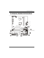
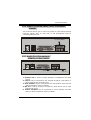
4. Jumpers, Headers & Connectors
JATXPWR1
JATXPWR2
JAUXPWR1
JAUX1
1
JWOL1
1
JUSB2
2
9
10
1
JPANEL1
JUSB3
2
9
10
1
JCMOS1
1
FDD1
IDE1-2
JDIMMVOLT
1
2
7
8
J1394C1
2
9
10
1
J1394A1
J1394B1
2
9
10
1
2
9
10
1
IDE3
Serial ATA Connector (JSATA1)
Serial ATA Connector (JSATA2)

Mainboard Features
9
4-1. Front Panel Connector: JPANEL1
Pin
Assignment
Function Pin
Assignment
Function
No.
No.
1 +5V 2 Sleep Control Sleep
3 NA Speaker 4 Ground Button
5 NA Connector 6 NA
NA
7 Speaker 8 Power LED (+)
9 HDD LED (+) Hard Drive 10 Power LED (+)
POWER
11 HDD LED (-) LED 12 Power LED (-) LED
13 Ground Reset 14 Power Button Power-on
15 Reset Control Button 16 Ground Button
17 NA 18 KEY
19 NA IrDA 20 KEY IrDA
21 +5V Connector 22 Ground Connector
23 IRTX 24 IRRX
SPK (Speaker Connector)
An offboard speaker can be installed on the motherboard as a
manufacturing option. An offboard speaker can be connected to the
motherboard at the front panel connector. The speaker (onboard or
offboard) provides error beep code information during the Power On
Self-Test when the computer cannot use the video interface. The
speaker is not connected to the audio subsystem and does not receive
output from the audio subsystem.
RST (Reset Button)
This connector can be attached to a momentary SPST switch. This
switch is usually open and when closed will cause the motherboard to
reset and run the POST (Power On Self Test).

Mainboard Features
10
POW-LED (Power LED Connector)
This connector can be attached to an LED on the front panel of a
computer case. The LED will illuminate while the computer is powered
on.
HLED (Hard Drive LED Connector)
This connector can be attached to an LED on the front panel of a
computer case. The LED will flicker during disk activity. This disk
activity only applies to those IDE drives directly attached to the system
board.
IR (Infrared Connector)
This connector is used to attach to an infrared sensing device. After the
IrDA interface is configured, connectionless data transfer to and from
portable devices such as laptops, PDAs is possible.
SLP (Sleep/Green Button)
This connector is used to conserve energy by powering down the
monitor and the hard disk when not in use. To configure this option,
you need to connect a button from the front panel to this connector.
Depressing the button will power down the monitor and hard drives
until the system is invoked by any keyboard activity, mouse activity,
modem activity or when the sleep button is depressed again. APM
(Advanced Power Management) must be enabled in the system BIOS
and the APM driver must be loaded.
ON/OFF (Power Button)
This connector can be attached to a front panel power switch. The
switch must pull the Power Button pin to ground for at least 50 ms to
signal the power supply to switch on or off. (The time required is due to
internal debounce circuitry on the system board). At least two seconds
must pass before the power supply will recognize another on/off signal.

Mainboard Features
11
4-2. ATX 20-pin Power Connector: JATXPWR1
PIN Assignment PIN Assignment
1 +3.3V 11 +3.3V
2 +3.3V 12 -12V
3 Ground 13 Ground
4 +5V 14 PS_ON
5 Ground 15 Ground
6 +5V 16 Ground
7 Ground 17 Ground
8 PW_OK 18 -5V
9 +5V_SB 19 +5V
10 +12V 20 +5V
4-3. ATX 12V Power Connector: JATXPWR2
PIN Assignment
PIN Assignment
1 +12V 3 Ground
2 +12V 4 Ground

Mainboard Features
12
4-4. Hard Disk Connectors: IDE1/IDE2/IDE3
This mainboard has a 32-bit Enhanced PCI IDE Controller that provides
PIO Mode 0~4, Bus Master, and Ultra DMA 33, Ultra DMA 66,Ultra DMA
100, Ultra DMA 133 (only for IDE1 and IDE2) functionality. It has two
HDD connectors IDE1 (primary) and IDE2 (secondary).
• IDE1 (Primary IDE Connector)
The first hard drive should always be connected to IDE1. IDE1 can
connect a Master and a Slave drive. You must configure the second
hard drive on IDE1 to Slave mode by setting the jumper accordingly.
• IDE2 (Secondary IDE Connector)
The IDE2 controller can also support a Master and a Slave drive. The
configuration is similar to IDE1. The second drive on this controller
must be set to slave mode.
• IDE3 (Optional)
This connector supports IDE3 cofiguration through the onboard Serial
ATA controler chip. You can use the IDE feature to set up a disk array
cofiguration and to support additional IDE devices. You can install a
hard disk (only in master mode) with this connector.
4-5. Floppy Disk Connector: FDD1
The motherboard provides a standard floppy disk connector (FDC) that
supports 360K, 720K, 1.2M, 1.44M and 2.88M floppy disk types. This
connector supports the provided floppy drive ribbon cables.
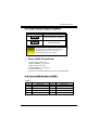
4-6. Wake On LAN Header: JWOL1
Pin No. Assignment
1
+5V_SB
2 Ground
3
Wake up

Mainboard Features
13
4-7. Clear CMOS Jumper: JCMOS1
JCMOS1 Assignment
1 3
1-2 Closed
Normal Operation (default)
1 3
2-3 Closed
Clear CMOS Data
※ Clear CMOS Procedures:
1. Remove AC power line.
2. Make JCMOS1 (2-3) closed.
3. Wait for five seconds.
4. Make JCMOS1 (1-2) closed.
5. Let AC power on.
6. Reset your desired password or clear the CMOS data.
4-8. Front USB Header: JUSB3
(JUSB3)
Pin Assignment Pin Assignment
1 +5V(fused) 2 +5V(fused)
3 USBP2- 4 USBP3-
5 USBP2+ 6 USBP3+
7 Ground 8 Ground
9 KEY 10 NC
The following procedures are for resetting
the BIOS password. It is important to
follow these instructions closely.

Mainboard Features
14
4-9. Front USB Header: JUSB2
(JUSB2)
Pin Assignment Pin Assignment
1 +5V(fused) 2 +5V(fused)
3 USBP2- 4 USBP3-
5 USBP2+ 6 USBP3+
7 Ground 8 Ground
9 KEY 10 NC
4-10. DDR DIMM Voltage: JDIMMVOLT
(Optional)
Pin DDR DIMM Voltage
1-2 2.5V
3-4 2.6V
5-6 2.7V
7-8 2.8V
If you meet the DDR DIMM compatible program, try to adjust the DDR
Voltage to fix the compatible program.
4-11. AUX Power Connector: JAUXPWR1
PIN Assignment
PIN Assignment
1 +12V 3 Ground
2 Ground 4 +5V
4-12. Front 1394 Header: J1394A1(Optional)
Pin Assignment Pin Assignment
1 A+ 2 A-
3 Ground 4 Ground
5 B+ 6 B-
7 +12V 8 +12V
9 KEY 10 NA

Mainboard Features
15
4-13. Front 1394 Header: J1394B1(Optional)
Pin Assignment Pin Assignment
1 A+ 2 A-
3 Ground 4 Ground
5 B+ 6 B-
7 +12V 8 +12V
9 KEY 10 NA
4-14. Front 1394 Header: J1394C1(Optional)
Pin Assignment Pin Assignment
1 A+ 2 A-
3 Ground 4 Ground
5 B+ 6 B-
7 +12V 8 +12V
9 KEY 10 NA
4-15. Aux Audio in Connector: JAUX1 (Optional)
Pin Assignment
1 Right channel AUX-in
2 Ground
3 Ground
4 Left channel AUX-in
4-16. Serial ATA Connector: JSATA1/ JSATA2
(Optional)
The motherboard has a PCI to SATA Controller with 2 channels SATA
interface, it satisfies the SATA 1.0 spec and can transfer data with
1.5GHz speed. For more details, please refer to page 35 (FastTrak
376).
Pin Assignment Pin Assignment
1 Ground 2 TXP+
3 TXN+ 4 Ground
5 RXN- 6 RXP+
7 Ground

Mainboard Features
16
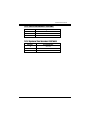
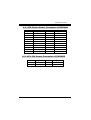
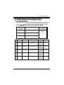
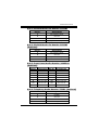
5. RAM Module Configuration
5-1. DDR SDRAM
DRAM Access Time: 2.5V Unbuffered DDR SDRAM (without ECC)
PC1600/ PC2100/ PC2700 Type required.
DRAM Type:128MB/256MB/512MB/1GBDIMM Module(184pin)
Total Memory Size with unbuffer DIMMs
(Only for reference)
DIMM Socket
Location
DDR Module Total Memory
Size (MB)
DIMM 1 64MB/128MB/256MB/512MB/1GB
*1
DIMM 2 64MB/128MB/256MB/512MB/1GB
*1
Max is
3GB
DIMM 3 64MB/128MB/256MB/512MB/1GB
*1
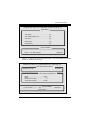
List of the status of DDR 400 already passed
Clock Vender Serial No. (Chip) Module
Size
MEMTEST
1 DDR400 KINGMAX KDL684T4AA-50 Double
Size
256M x2
Pass
2 DDR400 SAMSUNG K4H560838D-TCC4 Single
Size
256M x3
Pass
3 DDR400 TwinMOS TMD7608F8E50B Single
Size
256M x3
Pass
4 DDR400 Winbond W942508BH-5 Single
Size
256M x3
Pass
5 DDR400 Winbond W942508BH-5 Double
Size
512M x3
Pass

Mainboard Features
17
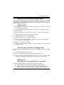
5-2. DIMM Module Configuration
1. The DIMM socket has a “Plastic Safety Tab” and the DIMM
memory module has an asymmetrical notch”, so the DIMM memory
module can only fit into the slot in one direction.
2. Push the tabs out. Insert the DIMM memory modules into the socket
at a 90-degree angle then push down vertically so that it will fit into
place.
3. The Mounting Holes and plastic tabs should fit over the edge and
hold the DIMM memory modules in place.
Page is loading ...
Page is loading ...
Page is loading ...
Page is loading ...
Page is loading ...
Page is loading ...
Page is loading ...
Page is loading ...
Page is loading ...
Page is loading ...
Page is loading ...
Page is loading ...
Page is loading ...
Page is loading ...
Page is loading ...
Page is loading ...
Page is loading ...
Page is loading ...
Page is loading ...
Page is loading ...
Page is loading ...
Page is loading ...
Page is loading ...
Page is loading ...
Page is loading ...
Page is loading ...
Page is loading ...
Page is loading ...
Page is loading ...
Page is loading ...
Page is loading ...
Page is loading ...
Page is loading ...
Page is loading ...
Page is loading ...
-
 1
1
-
 2
2
-
 3
3
-
 4
4
-
 5
5
-
 6
6
-
 7
7
-
 8
8
-
 9
9
-
 10
10
-
 11
11
-
 12
12
-
 13
13
-
 14
14
-
 15
15
-
 16
16
-
 17
17
-
 18
18
-
 19
19
-
 20
20
-
 21
21
-
 22
22
-
 23
23
-
 24
24
-
 25
25
-
 26
26
-
 27
27
-
 28
28
-
 29
29
-
 30
30
-
 31
31
-
 32
32
-
 33
33
-
 34
34
-
 35
35
-
 36
36
-
 37
37
-
 38
38
-
 39
39
-
 40
40
-
 41
41
-
 42
42
-
 43
43
-
 44
44
-
 45
45
-
 46
46
-
 47
47
-
 48
48
-
 49
49
-
 50
50
-
 51
51
-
 52
52
-
 53
53
-
 54
54
-
 55
55


Ask a question and I''ll find the answer in the document
Finding information in a document is now easier with AI
Related papers
Other documents
-
Gigabyte Promise RAID Function User manual
-
Albatron PM945GZ User manual
-
Promise Technology FastTrak SX8300 User manual
-
MATSONIC MS9127C User manual
-
Lindy 20689 User manual
-
 IWILL FB24624100 User manual
-
SIIG UltraATA 133 PCI RAID Installation guide
-
-
-
