
© 2018 NXP B.V.
FRDM-KW36 Minimum BoM Development
Board User’s Guide
1. Introduction
This guide describes the hardware of KW36 Minimum Bill
of Material development board (reference X-UBluetooth
LEKWZ0-31417). The board is configurable, low-power,
and cost-effective. It is an evaluation and development
board for application prototyping and demonstration of the
KW36A/35A and KW36Z/35Z family of devices.
The KW36 is an ultra-low-power, highly integrated single-
chip device that enables Bluetooth® Low Energy
(Bluetooth LE) or Generic FSK (at 250, 500 and 1000
kbps) for portable, extremely low-power embedded
systems.
The KW36 integrates a radio transceiver operating in
2.36 GHz to 2.48 GHz range supporting a range of GFSK,
an Arm® Cortex®-M0+ CPU, up to 512 KB Flash and up
to 64 KB SRAM. Bluetooth LE Link Layer hardware and
peripherals optimized to meet the requirements of the target
applications.
KW36 device is also available on the FRDM-KW36
Freedom Development Board. For more information about
the FRDM-KW36 Freedom Development Board, see the
NXP Semiconductor
Document Number: MiniBoMKW36UG
User’s Guide
Rev. 0
,
09/20187
Contents
1. Introduction ....................................................................... 1
2 Overview and description .................................................. 2
2.1 Overview .................................................................2
2.2 Feature description ..................................................3
3 Functional description........................................................ 5
3.1 Block diagram .........................................................5
3.2 Generic application schematic .................................6
3.3 RF Circuit ................................................................9
3.4 Clocks ......................................................................9
3.5 Power management ................................................ 10
3.6 User Application LEDs .......................................... 15
4 I/O .................................................................................... 16
4.1 I/O pin accessibility ............................................... 16
5 Schematic......................................................................... 18
6 Layout .............................................................................. 19
7 PCB ................................................................................. 20
8 Mounted PCB .................................................................. 20
9 Component positioning .................................................... 21
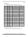
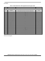
10 Bill of material ................................................................. 23
Buck mode ............................................................. 23
Bypass mode .......................................................... 25
11 References ....................................................................... 27
12 Revision history ............................................................... 27

Overview and description
FRDM-KW36 Minimum BoM Development Board User’s Guide, User’s Guide, Rev. 0, 09/20187
2 NXP Semiconductos.
FRDM-KW36 Freedom Development Board User's Guide (document FRDMKW36ZUG). Find the
schematic and design files at this link (NXP web page).
2 Overview and description
The KW36 minimum BoM development board is an evaluation environment supporting NXP
KW35Z/36Z/35A/36A (KW36) Wireless Microcontrollers (MCU). The KW36 integrates a radio
transceiver operating in the 2.4 GHz band (supporting a range of GFSK and Bluetooth LE) and an Arm
Cortex-M0+ MCU into a single package. NXP supports the KW36 with tools and software that include
hardware evaluation and development boards, software development IDE, applications, drivers, and a
custom PHY with a Bluetooth LE Link Layer. The KW36 minimum BoM development board (31417)
consists of the KW36Z device with a 32 MHz reference oscillator crystal, RF circuitry (including antenna),
supplied with a coin cell CR2032 or an external power supply. The board is a standalone PCB and supports
application development with NXP’s Bluetooth Low Energy and Generic FSK libraries.
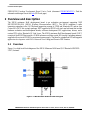
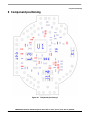
2.1 Overview
Figure 1 is a high-level block diagram of the KW36 Minimum BoM board (X-UBluetooth LEKWZ0-
31417) features:
Figure 1. KW36 Minimum BoM board block diagram

Overview and description
FRDM-KW36 Minimum BoM Development Board User’s Guide, User’s Guide, Rev. 0, 09/20187
NXP Semiconductors 3
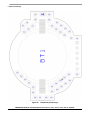
2.2 Feature description
The KW36 Minimum BoM development board is based on TPMS development platform. It is the most
diverse reference design containing the KW36Z device and all necessary I/O connections to use as a stand-
alone board. Figure 2 shows the KW36 Minimum BoM development board.
Figure 2. KW36 Minimum BoM development board
The KW36 Minimum BoM development board includes following features:
• NXP’s ultra-low-power KW36Z Wireless MCU supporting Bluetooth LE and Generic FSK
• Reference design area with small-footprint, low-cost RF node:
o Single-ended input/output port
o Very low count of external components (minimum BoM)
• Ceramic antenna
• Selectable power sources (coin cell or external output power)
• DC-DC converter with Buck, and Bypass operation modes
• 32 MHz reference oscillator for RF operation
• 32.768 kHz reference oscillator mainly use for RTC operation and RF low-power operation
• 2.4 GHz frequency operation (ISM and MBAN)
• Coin cell connector to be able to work using a CR2032 coin cell
• Cortex 10-pin (0.05) SWD debug port for target MCU
• 1x6 Connector 6-pin UART port
• Three orange LED indicator for power and communication
• 20 available GPIOs


Functional description
FRDM-KW36 Minimum BoM Development Board User’s Guide, User’s Guide, Rev. 0, 09/20187
NXP Semiconductors 5
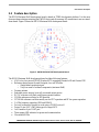
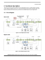
3 Functional description
The four-layer board provides the KW36 with its required RF circuitry, 32 MHz reference oscillator
crystal, and power supply with a DC-DC converter including Bypass and Buck (default) modes. The
layout for this base-level functionality can be used as a reference layout for your target board.
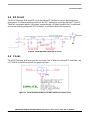
3.1 Block diagram
Figure 4. Block diagram (Buck mode)
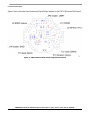
Figure 5. Block diagram (Bypass mode)

Functional description
FRDM-KW36 Minimum BoM Development Board User’s Guide, User’s Guide, Rev. 0, 09/20187
6 NXP Semiconductos.
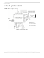
3.2 Generic application schematic
3.2.1 Buck mode (auto-start)
Figure 6. Buck mode (auto start)

Functional description
FRDM-KW36 Minimum BoM Development Board User’s Guide, User’s Guide, Rev. 0, 09/20187
NXP Semiconductors 7
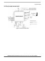
3.2.2 Buck mode (manual-start)
Figure 7. Buck mode (manual start)

Functional description
FRDM-KW36 Minimum BoM Development Board User’s Guide, User’s Guide, Rev. 0, 09/20187
8 NXP Semiconductos.
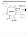
3.2.3 Bypass mode
Figure 8. Bypass mode

Functional description
FRDM-KW36 Minimum BoM Development Board User’s Guide, User’s Guide, Rev. 0, 09/20187
NXP Semiconductors 9
3.3 RF Circuit
The KW36 Minimum BoM board RF circuit provides an RF interface for users to begin application
development. A minimum matching network to the MCU antenna pin is provided through C17 and L8.
Those two components match to the ceramic antenna through a 50 ohms controlled line. An additional
and optional matching component (R112 footprint), is provided to better filter harmonics.
Figure 9. KW36 Minimum BoM board RF circuit
3.4 Clocks
The KW36 Minimum BoM board provides two clocks. One 32 MHz for clocking MCU and Radio, and
a 32.768 kHz to provide an accurate low-power time base.
Figure 10. KW36 minimum BoM board 32 MHz reference oscillator circuit

Functional description
FRDM-KW36 Minimum BoM Development Board User’s Guide, User’s Guide, Rev. 0, 09/20187
10 NXP Semiconductos.
• 32 MHz Reference Oscillator
o Figure 10 shows the 32 MHz external crystal Y3. The KW36Z requires the frequency to
be accurate less than 10 ppm. For more details, please refer to the device datasheet.
o Internal load capacitors provide the crystal load capacitance. The internal load capacitor
is adjustable which allows the center frequency of the crystal to be tuned.
o To measure the 32 MHz oscillator frequency, program the CLKOUT (PTB0) signal to
provide buffered output clock signal (TP29).
Figure 11. KW36 Minimum BoM Board 32.786 kHz oscillator circuit
• 32.768 kHz Crystal Oscillator (for accurate low-power time base)
o A secondary 32.768 kHz crystal QZ1 is provided (see Figure 6)
o Internal load capacitors provide the entire crystal load capacitance
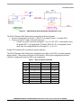
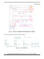
3.5 Power management
There are two different ways to power the KW36 Minimum BoM board. The KW36 Minimum BoM
board power-management circuit is shown in Figure 12:

Functional description
FRDM-KW36 Minimum BoM Development Board User’s Guide, User’s Guide, Rev. 0, 09/20187
NXP Semiconductors 11
Figure 12. KW36 Minimum BoM Board power management circuit.
The KW36 Minimum BoM Board can be powered by the following means:
• From an external battery (Coin-cell – CR2032). Use jumper J4 pins 1-2 or solder R234.
• From an external DC supply in the following ways:
o Connect two wires: a wire that can supply 1.71 to 3.6 VDC (BT1-1) and another wire to
the ground (BT1-2) in bypass mode. By default, KW36 DC-DC is configured in buck
mode, then, the voltage should be in the range of 2.1 V to 3.6 V.
Orange LED marked as D4 is available as a power indicator.
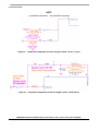
The KW36 Minimum BoM Board can be configured to use either of the DCDC converter operating
modes (default). These modes are Bypass or Buck (default). Moving the configuration from buck
(default) to bypass mode need to modify some components:
Table 1. : Buck or bypass mode table
Buck mode
Bypass mode
Figure
R1
x
-
10
R2
-
x
10
R3
-
x
10
R4
x
-
10
R5
-
x
9
R6
x
-
9
R7
-
x
10
R9
x
x
8
R10
-
-
8
L3
x
-
8

Functional description
FRDM-KW36 Minimum BoM Development Board User’s Guide, User’s Guide, Rev. 0, 09/20187
12 NXP Semiconductos.
NOTE
x (populated component), - not populated component
Figure 13. Component configuration for Buck or Bypass mode – DCDC_CFG pin
Figure 14. Component configuration for Buck or Bypass mode – PSWITCH pin


Functional description
FRDM-KW36 Minimum BoM Development Board User’s Guide, User’s Guide, Rev. 0, 09/20187
14 NXP Semiconductos.
VREFH/VREF_OUT
Circuit for VREF_OUT
VREF_OUT provides a 1.2V reference voltage that can be used as VREFH for ADC.
Figure 17. Circuit for VREF_OUT
Circuit for VREFH
VREFH is the high reference voltage for the ADC, in this circuit it will have the same values as
VDDA (Analog supply voltage).
Figure 18. Circuit for VREFH

Functional description
FRDM-KW36 Minimum BoM Development Board User’s Guide, User’s Guide, Rev. 0, 09/20187
NXP Semiconductors 15
3.6 User Application LEDs
The KW36 Minimum BoM Board provides an orange LED for user applications. Figure 19 shows the
circuitry for the application controlled LEDs.
- LED_COM1: SCL
- LED_COM2: SDA
- LED_COM3: RF active
Figure 19. KW36 Minimum BoM Board Orange LED circuit.
NOTE
When operating in default Buck configuration, the MCU would be
operating at 1.8 V, which means that GPIO would be operating at 1.8 V.

I/O
FRDM-KW36 Minimum BoM Development Board User’s Guide, User’s Guide, Rev. 0, 09/20187
16 NXP Semiconductos.
4 I/O
4.1 I/O pin accessibility
Figure 20 shows the I/O pinout (TPx). Each I/O pin has its own ground to facilitate the 2 wires
connection on the PCB.
Figure 20. KW36 Minimum BoM Board I/O pinout

I/O
FRDM-KW36 Minimum BoM Development Board User’s Guide, User’s Guide, Rev. 0, 09/20187
NXP Semiconductors 17
Table 2 shows the signals that can be multiplexed to each pin.
Table 2. Test point description
TPx
Test Point (TPx)- Description
IC
Pin
TP20
PTA16/LLWU_P4/SPI1_SOUT/UART1_RTS_b/TPM0_CH0
4
TP21
PTC18/LLWU_P2/SPI0_IN/I2C1_SDA/UART0_TX/BSM_DATA/DTM_TX/UART1_TX
47
TP22
PTC17/LLWU_P1/RF_EXT_OSC_EN/SPI0_SOUT/I2C1_SCL/UART0_RX/BSM_FRAME/DTM_RX/UART1_RX
46
TP23
PTC19/LLWU_P3/RF_EARLY_WARNING/SPI0_PCS0/I2C0_SCL/UART0_CTS_b/BSM_CLK/UART1_CTS_b
48
TP25
PTC16/LLWU_P0/SPI0_SCK/I2C0_SDA/UART0_RTS_b/TPM0_CH3/UART1_RTS_b
45
TP26
PTC1/DIAG1/RF_EARLY_WARNING/ANT_B/I2C0_SDA/UART0_RTS_b/TPM0_CH2/SPI1_SCK/BSM_CLK
37
TP27
PTC2/LLWU_P10/TSI0_CH14/DIAG1/TX_SWITCH/I2C1_SCL/UART0_RX/CMT_IRO/DTEST6/DTM_RX
38
TP28
PTC3/DIAG3/LLWU_P11/RX_SWITCH/I2C1_SDA/UART0_TX/TPM0_CH1/DTM_TX/SPI1_SIN/CAN0_TX
39
TP29
PTB0/LLWU_P8/RF_RFOSC_EN/RF_DFT_RESET/I2C0_SCL/CMP0_OUT/TPM0_CH1/CLKOUT/CAN0_TX
16
TP30
PTB1/ADC0_SE1/CMP0_IN5/RF_PRIORITY/DTM_RX/I2C0_SDA/LPTMR0_ALT1/TPM0_CH2/CMT_IRO/CAN0_RX
17
TP31
PTC4/DIAG4/RF_ACTIVE/LLWU_P12/ANT_A/EXTRG_IN/UART0_CTS_b/TPM1_CH0/BSM_DATA/SPI1_PCS0/CAN0_RX
40
TP32
PTC5/LLWU_P13/RF_RF_OFF/ LPTMR0_ALT2/UART0_RTS_b/TPM1_CH1/BSM_CLK
41
TP34
PTA17/LLWU_P5/RF_DFT_RESET/SPI1_SIN/UART1_RX/CAN0_TX/TPM_CLKIN1
5
TP35
PTA18/LLWU_P6/SPI1_SCK/ UART1_TX/CAN0_RX/TPM2_CH0
6
TP36
PTA19/ADC0_SE5/LLWU_P7/SPI1_PSC0/UART1_CTS_b/TMP2_CH1
7
TP37
PTB2/ADC0_SE3/CMP0_IN3/RF_OFF/TPM1_CH0/DTEST13/DCDC_TESTO5
18
TP38
PTB3/ADC0_SE2/CMP0_IN4/CLKOUT/TPM1_CH1/DTEST9/RTC_CLKOUT/ERCLK32K
19
TP42
PTB18/DAC0_OUT/ADC0_SE4/CMP0_IN2/I2C1_CLK/TPM_CLKIN0/TPM0_CH0/DTEST8/NMI
23
TP46
ADC0_DP0/CMP0_IN0
24
TP47
ADC0_DP0/CMP0_IN1
25
Table 3. UART connector pinout (JP3)
HDR Pin
1x6 Connector (JP3) - Description
IC Pin
1
GND
-
2
FTDI cable CTS / PTC5
41
3
FTDI cable VCC / VBAT_PWR
-
4
FTDI cable TXD / UART0_RX
42
5
FTDI cable RXD / UART0_TX
43
6
FTDI cable RTS / PTC4
40
Table 4. SWD connector pinout (J14)
HDR Pin
2x5 Connector (J14) - Description
IC Pin
1
VDD_1P8F
-
2
PTA0_SWD_DIO
1
3
GND
-
4
PTA1_SWD_CLK
2
5
GND
-
6
NC
-
7
NC
-
8
NC
-
9
NC
-
10
RST_TGTMCU_b
3

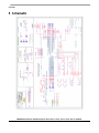
Schematic
FRDM-KW36 Minimum BoM Development Board User’s Guide, User’s Guide, Rev. 0, 09/20187
18 NXP Semiconductos.
5 Schematic

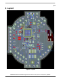
Layout
FRDM-KW36 Minimum BoM Development Board User’s Guide, User’s Guide, Rev. 0, 09/20187
NXP Semiconductors 19
6 Layout
Figure 21. Layout

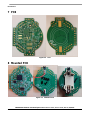
Mounted PCB
FRDM-KW36 Minimum BoM Development Board User’s Guide, User’s Guide, Rev. 0, 09/20187
20 NXP Semiconductos.
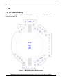
7 PCB
Figure 22. PCB
8 Mounted PCB
Figure 23. Mounted PCB
Page is loading ...
Page is loading ...
Page is loading ...
Page is loading ...
Page is loading ...
Page is loading ...
Page is loading ...
Page is loading ...
-
 1
1
-
 2
2
-
 3
3
-
 4
4
-
 5
5
-
 6
6
-
 7
7
-
 8
8
-
 9
9
-
 10
10
-
 11
11
-
 12
12
-
 13
13
-
 14
14
-
 15
15
-
 16
16
-
 17
17
-
 18
18
-
 19
19
-
 20
20
-
 21
21
-
 22
22
-
 23
23
-
 24
24
-
 25
25
-
 26
26
-
 27
27
-
 28
28


NXP FRDM-KW36 User manual
- Type
- User manual
- This manual is also suitable for
Ask a question and I''ll find the answer in the document
Finding information in a document is now easier with AI
Related papers
Other documents
-
NXP Semiconductors FRDM-MC-LVPMSM User manual
-
Topcom 10003080 Datasheet
-
Freescale Semiconductor FRDM-KL03Z User manual
-
Norton R222 38x25m Handy Rolls User manual
-
Norton R222 User manual
-
-
-
Norton R222-50x25m Handy Rolls User manual
-
-
Dunlop QZ1 User manual