Texas Instruments bq76200EVM User guide

Type
User guide
User's Guide
SLVU926July 2015
bq76200 High Voltage Battery Pack Front-End
Charge/Discharge High-Side NFET Driver Evaluation
Module
This evaluation module (EVM) is a complete evaluation system for the bq76200 High Voltage Battery
Pack Front-End Charge/Discharge High-Side NFET Driver. The EVM includes one bq76200 and FETs to
control current in a configuration typical for switching current in a lithium-ion battery pack. The circuit
module includes one bq76200 integrated circuit (IC), two CSD19351Q5A FETs, and all other onboard
components necessary to switch charge, discharge, and precharge current and to monitor the output pack
voltage. The circuit module connects between a "battery" source and a "pack" load. With the on-board
jumpers or external control, the user can switch the FETs to evaluate the overall functionality of the
solution under different charge and discharge conditions.
Contents
1 Features....................................................................................................................... 4
1.1 Kit Contents.......................................................................................................... 4
1.2 Ordering Information ............................................................................................... 4
1.3 Documentation ...................................................................................................... 4
1.4 bq76200 Circuit Module Performance Specification Summary............................................... 4
2 bq76200EVM Quick Start Guide........................................................................................... 4
2.1 Before You Begin................................................................................................... 4
2.2 Items Needed for EVM Quick Start Evaluation ................................................................. 5
2.3 EVM Connections................................................................................................... 5
2.4 Quick Start Sequence.............................................................................................. 6
3 Additional Evaluation Setups............................................................................................... 7
3.1 Operation With Charge and Discharge Currents ............................................................... 7
3.2 Connecting to a BMS System..................................................................................... 7
3.3 Connecting to a MCU .............................................................................................. 8
3.4 Troubleshooting..................................................................................................... 8
4 bq76200EVM Circuit Module Schematic ................................................................................. 9
4.1 Alternate FETs ...................................................................................................... 9
4.2 Heatsink Patterns................................................................................................... 9
4.3 PACK Transient Pattern ........................................................................................... 9
4.4 Input Limit Circuit ................................................................................................... 9
5 Circuit Module Physical Layouts ......................................................................................... 10
5.1 Board Layout....................................................................................................... 10
5.2 Schematic .......................................................................................................... 14
6 Bill of Materials ............................................................................................................. 15
7 Related Documentation from Texas Instruments ...................................................................... 16
List of Figures
1 bq76200 Circuit Module Connection for Simple Demonstration....................................................... 5
2 Bipolar Operation ............................................................................................................ 7
3 Operation with a BMS....................................................................................................... 8
4 Operation With a MCU...................................................................................................... 8
5 Top Silk Screen............................................................................................................. 10
6 Bottom Silk Screen......................................................................................................... 10
1
SLVU926July 2015 bq76200 High Voltage Battery Pack Front-End Charge/Discharge High-Side
NFET Driver Evaluation Module
Submit Documentation Feedback
Copyright © 2015, Texas Instruments Incorporated
www.ti.com
7 Top Assembly............................................................................................................... 11
8 Bottom Assembly........................................................................................................... 11
9 Top Layer.................................................................................................................... 12
10 Internal Layer 1............................................................................................................. 12
11 Internal Layer 2............................................................................................................. 13
12 Bottom Layer................................................................................................................ 13
13 bq76200EVM Schematic.................................................................................................. 14
List of Tables
1 Performance Specification Summary ..................................................................................... 4
2 bq76200EVM Bill of Materials ........................................................................................... 15
2
bq76200 High Voltage Battery Pack Front-End Charge/Discharge High-Side SLVU926July 2015
NFET Driver Evaluation Module
Submit Documentation Feedback
Copyright © 2015, Texas Instruments Incorporated
www.ti.com
General Texas Instruments High Voltage Evaluation (TI HV EVM) User Safety Guidelines
WARNING
Always follow TI’s set-up and application instructions, including use of all interface components within their
recommended electrical rated voltage and power limits. Always use electrical safety precautions to help
ensure your personal safety and the safety of those working around you. Contact TI’s Product Information
Center http://support/ti./com for further information.
Save all warnings and instructions for future reference.
Failure to follow warnings and instructions may result in personal injury, property damage, or
death due to electrical shock and/or burn hazards.
The term TI HV EVM refers to an electronic device typically provided as an open framed, unenclosed
printed circuit board assembly. It is intended strictly for use in development laboratory environments,
solely for qualified professional users having training, expertise, and knowledge of electrical safety risks in
development and application of high-voltage electrical circuits. Any other use and/or application are strictly
prohibited by Texas Instruments. If you are not suitably qualified, you should immediately stop from further
use of the HV EVM.
1. Work Area Safety:
(a) Keep work area clean and orderly.
(b) Qualified observer(s) must be present anytime circuits are energized.
(c) Effective barriers and signage must be present in the area where the TI HV EVM and its interface
electronics are energized, indicating operation of accessible high voltages may be present, for the
purpose of protecting inadvertent access.
(d) All interface circuits, power supplies, evaluation modules, instruments, meters, scopes and other
related apparatus used in a development environment exceeding 50 V
RMS
/75 VDC must be
electrically located within a protected Emergency Power Off (EPO) protected power strip.
(e) Use a stable and non-conductive work surface.
(f) Use adequately insulated clamps and wires to attach measurement probes and instruments. No
freehand testing whenever possible.
2. Electrical Safety:As a precautionary measure, it is always a good engineering practice to assume that
the entire EVM may have fully accessible and active high voltages.
(a) De-energize the TI HV EVM and all its inputs, outputs, and electrical loads before performing any
electrical or other diagnostic measurements. Revalidate that TI HV EVM power has been safely de-
energized.
(b) With the EVM confirmed de-energized, proceed with required electrical circuit configurations, wiring,
measurement equipment hook-ups and other application needs, while still assuming the EVM circuit
and measuring instruments are electrically live.
(c) Once EVM readiness is complete, energize the EVM as intended.
WARNING: while the EVM is energized, never touch the EVM or its electrical circuits as they
could be at high voltages capable of causing electrical shock hazard.
3. Personal Safety:
(a) Wear personal protective equipment, for example, latex gloves and/or safety glasses with side
shields or protect EVM in an adequate lucent plastic box with interlocks from accidental touch.
4. Limitation for Safe Use:
(a) EVMs are not to be used as all or part of a production unit.
3
SLVU926July 2015 bq76200 High Voltage Battery Pack Front-End Charge/Discharge High-Side
NFET Driver Evaluation Module
Submit Documentation Feedback
Copyright © 2015, Texas Instruments Incorporated
!
Features
www.ti.com
1 Features
Complete evaluation system for the bq76200 High Voltage Battery Pack Front-End Charge/Discharge
High-Side NFET Driver IC
Populated circuit module for quick setup
1.1 Kit Contents
bq76200 circuit module
1.2 Ordering Information
The EVM orderable part number is bq76200EVM-606. For complete ordering information, see the product
page at www.ti.com.
1.3 Documentation
See the device data sheet for bq76200 (SLUSC16) on www.ti.com for information on device hardware.
1.4 bq76200 Circuit Module Performance Specification Summary
This section summarizes the performance specifications of the bq76200EVM.
Table 1. Performance Specification Summary
Specification Minimum Typical Maximum Unit
Input voltage BATT+ to BATSR– 10 n/a 70 V
Output voltage PACK+ to PACK- 0 n/a 70 V
Charge and discharge current 0 2 15 A
Operating temperature 20 25 30
o
C
2 bq76200EVM Quick Start Guide
This section provides the step-by-step procedures required to use a new EVM and configure it for
operation in a laboratory environment.
2.1 Before You Begin
The following warnings and cautions are noted for the safety of anyone using or working close to the
bq76200 EVM. Observe all safety precautions.
Warning Warning Hot surface. Contact may cause burns. Do not touch.
Caution Do not leave EVM powered when unattended.
Danger High The bq76200 EVM does not have an isolation boundary. If you apply high
Voltage voltage to this board, all terminals should be considered high voltage.
spacer
Electric shock is possible when connecting the board to live wire. The
board should be handled with care by a professional.
spacer
For safety, use of isolated test equipment with overvoltage and
overcurrent protection is highly recommended.
4
bq76200 High Voltage Battery Pack Front-End Charge/Discharge High-Side SLVU926July 2015
NFET Driver Evaluation Module
Submit Documentation Feedback
Copyright © 2015, Texas Instruments Incorporated
Rload
DC Power Supply
+ -
³EDWWHU\´
www.ti.com
bq76200EVM Quick Start Guide
CAUTION
The circuit module has signal traces and component leads on the bottom of the
board. This may result in exposed voltages, hot surfaces, or sharp edges. Do
not reach under the board during operation.
CAUTION
The circuit module may be damaged by overtemperature. To avoid damage,
monitor the temperature during evaluation and provide cooling, as needed, for
your system environment.
CAUTION
Some power supplies can be damaged by application of external voltages. If
using more than one power supply, check your equipment requirements and
use blocking diodes or other isolation techniques, as needed, to prevent
damage to your equipment.
CAUTION
The circuit module is not a finished product or electrical appliance. The module
does not contain current or voltage thresholds for circuit protection. It must be
used by qualified personnel with additional equipment for evaluation only.
2.2 Items Needed for EVM Quick Start Evaluation
bq76200 circuit module
A DC power supply that can provide 10 V and 1 A minimum (a voltage range, bipolar operation, and
constant current constant voltage capability is desirable)
A load such as a 100-kΩ 1/4-W or other suitable resistor
A DC meter or measurement instrument
Suitable cables for connection
2.3 EVM Connections
This section covers the hardware connections for the EVM (see Figure 1).
Figure 1. bq76200 Circuit Module Connection for Simple Demonstration
Supply terminals (BATT+, BATSR–)
These are the supply terminals for the board. BATT+ is the positive terminal of the battery or supply,
5
SLVU926July 2015 bq76200 High Voltage Battery Pack Front-End Charge/Discharge High-Side
NFET Driver Evaluation Module
Submit Documentation Feedback
Copyright © 2015, Texas Instruments Incorporated
bq76200EVM Quick Start Guide
www.ti.com
BATSR– is the negative terminal of the power supply or after the sense resistor. When using a power
supply for evaluation, be sure the power supply can accept or is protected from any reverse current
such as with a blocking diode if another supply is used in the system.
Pack terminals (PACK+ and PACK–)
Attach the load or charger to the pack terminals. If using a power supply to simulate a charger, be sure
it can accept or is protected from any reverse current.
Ground shunt (J3)
This shunt connects the IC VSS to the high-current return path. When the shunt is removed, the two
signals are connected with a 1-kΩ resistor.
Control voltage shunt (J6)
This shunt connects BATT+ to a zener regulator to provide an on-board control voltage for simple
evaluation.
Control input header (J7)
J7 allows enabling the bq76200 control signals from the on-board zener regulator voltage using shunts.
See the bq76200 data sheet for the description of the control signals. The divided pack voltage can
also be accessed here as the PDIV signal. When the shunts are not used, the header may be used for
connection to other equipment.
Control input terminal block (J8)
The J8 terminal block provides an alternate connection point for control inputs and PDIV signal.
2.4 Quick Start Sequence
These steps describe a simple demonstration or check of the operation of the bq76200EVM.
1. Connect a 100-kΩ resistor to the PACK terminals.
2. Confirm shunts are in place on J3, J6, and J7 at the PMON, CPEN, PCHG, CHG, and DSG positions.
3. Connect a 10-V power supply across the BATT+ and BATSR– terminals.
4. Enable the supply.
5. Measure the voltage on the pack terminals. Observe this is approximately 10 V.
6. Remove the shunt at the J7 CHG position. Observe that the pack voltage drops approximately 300 mV
below the supply. When using a smaller load resistor the voltage drop will be greater
7. Remove the shunt at the J7 PCHG position also. Observe that the pack voltage drops to approximately
500 mV below the supply. When using a smaller load resistor, this additional drop may not be
observed.
8. Re-install the CHG and PCHG shunts.
9. Remove the shunt at the J7 DSG position. Observe that the pack voltage drops to approximately 0 V.
10. Measure the voltage on the PDIV pin J7 pin 3 or J8 pin 2. Observe that this voltage is approximately 0
V.
11. Re-install the shunt at the J7 DSG position. Observe that the PDIV voltage is approximately 0.36 V.
12. Remove the shunt at the J7 PMON position. Observer that the PDIV voltage drops to approximately 0
V.
13. Re-install the PMON shunt.
14. Disable the power supply and disconnect, if complete.
6
bq76200 High Voltage Battery Pack Front-End Charge/Discharge High-Side SLVU926July 2015
NFET Driver Evaluation Module
Submit Documentation Feedback
Copyright © 2015, Texas Instruments Incorporated
Csys
Bipolar Power
Supply
+ -
³EDWWHU\´
Bipolar Power
Supply
+ -
³FKDUJHU´
RU³ORDG´
Cload
www.ti.com
Additional Evaluation Setups
3 Additional Evaluation Setups
CAUTION
The bq76200 EVM does not contain capacitors on the input or output current
paths to dampen transients. Be sure to use appropriate capacitance (Csys and
Cload in the following diagrams) to avoid damage to the board from cable or
equipment transient responses during evaluation.
3.1 Operation With Charge and Discharge Currents
If bipolar power supplies are available, current control can be demonstrated through the board in both
directions, see Figure 2. A battery voltage in range must be applied to the BAT side of the EVM for
operation. The instrument on the PACK side can be used as a load if it is set to a lower voltage than the
battery side or as a charger if set to a higher voltage.
Figure 2. Bipolar Operation
3.2 Connecting to a BMS System
The bq76200 EVM may be connected to a BMS board so that the BMS device can provide the control
signals for the bq76200, a concept is shown in Figure 3. The J7 header or J8 terminal block may be useful
to connect signals to the bq76200 EVM, refer to the documentation for the BMS board to determine where
to connect and how to interface the signals. Ensure that the BMS settings are correctly changed to match
the pack and application for the solution being evaluated and the bq76200 EVM limits. The J6 shunt
should be removed since the BMS board will provide control signal levels. The pull-down resistor patterns
on the bq76200 EVM inputs may be populated, if needed, for the evaluation.
When connecting to the BMS board, the J3 shunt should be removed. The R1 resistor will be in parallel
with the sense resistor through the path of the signal ground connected at J7 or J8. Generally, this should
be OK since the current error would be 1 ppm with a 1-mΩ sense resistor or 10 ppm with a 10-mΩ
sense resistor. However, connect the board grounds as appropriate for the evaluation.
7
SLVU926July 2015 bq76200 High Voltage Battery Pack Front-End Charge/Discharge High-Side
NFET Driver Evaluation Module
Submit Documentation Feedback
Copyright © 2015, Texas Instruments Incorporated
DC Power Supply
+ -
Load
DC Power Supply
+ -
³EDWWHU\´
MCU
Voltage
Connect to
header or
terminal block,
as desired
MCU
Csys
Cload
Load
³EDWWHU\´
Supply or
Cell
Assembly
Connect to
header or
terminal block,
as desired
BMS Board
Csys
Rsense
Cload
+
-
Remove Ground
Shunt
Additional Evaluation Setups
www.ti.com
Figure 3. Operation with a BMS
3.3 Connecting to a MCU
It may be desired to evaluate the board with control from an MCU, see Figure 4. The J7 header or J8
terminal block may be useful to connect signals depending on the MCU board and cabling used. The J6
shunt should be removed since the MCU board should provide the control signals. Generally, it is
expected that the J3 shunt would be installed, but provide an appropriate ground for the system.
Figure 4. Operation With a MCU
3.4 Troubleshooting
If the bq76200 does not appear to be operating, check the BATT+ and enable voltages. BATT+ must be in
the range of the board and the BAT test point in the range of the IC as shown in the data sheet. Check
that the board ground is appropriately connected to the system supply ground. With the CP_EN voltage
applied in the 3 to 12 V or other range indicated in the data sheet, measure the voltage of the VDDCP
(TP7) with respect to BAT (TP9) and confirm it is within the range shown in the data sheet. The Quick
Start Sequence section is a good procedure to check the operation of the board.
8
bq76200 High Voltage Battery Pack Front-End Charge/Discharge High-Side SLVU926July 2015
NFET Driver Evaluation Module
Submit Documentation Feedback
Copyright © 2015, Texas Instruments Incorporated
www.ti.com
bq76200EVM Circuit Module Schematic
4 bq76200EVM Circuit Module Schematic
This section contains information on other EVM features.
4.1 Alternate FETs
The EVM has D2PAK and TO-220 footprints for power FETs as options for evaluation. A DPAK footprint
option is available as a precharge FET option.
4.2 Heatsink Patterns
The EVM is designed with copper plane areas to distribute heat on the board. The board has a hole
pattern for an optional bolt on heatsink H9 shown in the bill of materials. The board also has patterns on
the top layer for D2PAK heatsinks HS10 and HS11 shown in the bill of materials. The flat areas of the
back of the board may be used for adhesive mount heatsinks, if appropriate.
4.3 PACK Transient Pattern
D2 is a pattern for a TVS on the pack, if desired.
4.4 Input Limit Circuit
The bq76200 EVM contains zener diodes and resistors on the inputs. These may limit the voltage to the
control input pins if multiple pins on the IC are shorted together and the ground connection is maintained,
but do not provide a safety isolation boundary. The zeners are not intended for protection of the inputs to
the IC.
9
SLVU926July 2015 bq76200 High Voltage Battery Pack Front-End Charge/Discharge High-Side
NFET Driver Evaluation Module
Submit Documentation Feedback
Copyright © 2015, Texas Instruments Incorporated
Circuit Module Physical Layouts
www.ti.com
5 Circuit Module Physical Layouts
This section contains the printed-circuit board (PCB) layout, assembly drawings, and schematic for the
bq76200 circuit module.
5.1 Board Layout
This section shows the PCB layers and assembly drawing for the bq76200 module (see Figure 5 through
Figure 12).
Figure 5. Top Silk Screen
Figure 6. Bottom Silk Screen
10
bq76200 High Voltage Battery Pack Front-End Charge/Discharge High-Side SLVU926July 2015
NFET Driver Evaluation Module
Submit Documentation Feedback
Copyright © 2015, Texas Instruments Incorporated
www.ti.com
Circuit Module Physical Layouts
Figure 7. Top Assembly
Figure 8. Bottom Assembly
11
SLVU926July 2015 bq76200 High Voltage Battery Pack Front-End Charge/Discharge High-Side
NFET Driver Evaluation Module
Submit Documentation Feedback
Copyright © 2015, Texas Instruments Incorporated
Circuit Module Physical Layouts
www.ti.com
Figure 9. Top Layer
Figure 10. Internal Layer 1
12
bq76200 High Voltage Battery Pack Front-End Charge/Discharge High-Side SLVU926July 2015
NFET Driver Evaluation Module
Submit Documentation Feedback
Copyright © 2015, Texas Instruments Incorporated
www.ti.com
Circuit Module Physical Layouts
Figure 11. Internal Layer 2
Figure 12. Bottom Layer
13
SLVU926July 2015 bq76200 High Voltage Battery Pack Front-End Charge/Discharge High-Side
NFET Driver Evaluation Module
Submit Documentation Feedback
Copyright © 2015, Texas Instruments Incorporated
4
7,8
1,2,3
5,6,
Q4
4
7,8
1,2,3
5,6,
Q3
J4
J1 J2
J5
VDDCP
1
BAT
2
NC
3
CHG_EN
4
CP_EN
5
DSG_EN
6
PMON_EN
7
PCHG_EN
8
VSS
9
PACKDIV
10
PACK
11
DSG
12
NC
13
PCHG
14
NC
15
CHG
16
U1
BQ76200PW
1 2
3 4
5 6
7 8
9 10
11 12
13 14
J7
D1
0.1µF
C3
0.1µF
C4
0.1µF
C1
0.1µF
C2
Q5
DNP
Q6
DNP
11.3k
25 ppm/C
R36
10.0Meg
R31
DNP
10.0Meg
R32
DNP
10.0Meg
R33
DNP
10.0Meg
R34
DNP
10.0Meg
R35
DNP
10.0k
R11
10.0k
R12
10.0k
R13
10.0k
R14
10.0k
R15
0.01µF
C8
0.47µF
C6
300k
25 ppm/C
R26
100
R10
10.0Meg
R9
10.0Meg
R8
1.0k
R2
1.0k
R3
1.0k
R4
1.0k
R5
Q1
10.0Meg
R7
PACK-
PACK+
Output 10 - 70 V
15A max
BATSR-
BATT+
Input 10 - 70 V
D3
5.1V
D4
J6
100k
R6
0.01µF
C7
0.1µF
C5 100
R16
GND
GND
GND
GND GND
1.00k
R1
J3
0
R17
0
R18
0
R19
GND
GND
GND
Manual
D2
DNP
Operation
GND
Q7
DNP
Q8
DNP
Q2
DNP
TP7
TP9
TP8
TP10
TP11
TP12
TP13
TP2
TP4 TP5
TP1
TP14 TP15 TP16
TP3
TP6
E1
GND GND
GND
TP17
GND
1.00k
R20
39.2k
R21
39.2k
R23
39.2k
R25
39.2k
R28
39.2k
R30
D5 D6 D7 D8 D9 D10
GND
1.00k
R22
1.00k
R24
1.00k
R27
1.00k
R29
GND GND GND GND
CD
PGATE
BATT+ PACK+
PACK-
DGATECGATE
DSG
CHG
PCHG
CPEN
PMON
DIVP
Local
5
4
1
2
3
6
7
J8
Circuit Module Physical Layouts
www.ti.com
5.2 Schematic
Figure 13 shows the bq76200EVM schematic.
Figure 13. bq76200EVM Schematic
14
bq76200 High Voltage Battery Pack Front-End Charge/Discharge High-Side SLVU926July 2015
NFET Driver Evaluation Module
Submit Documentation Feedback
Copyright © 2015, Texas Instruments Incorporated
www.ti.com
Bill of Materials
6 Bill of Materials
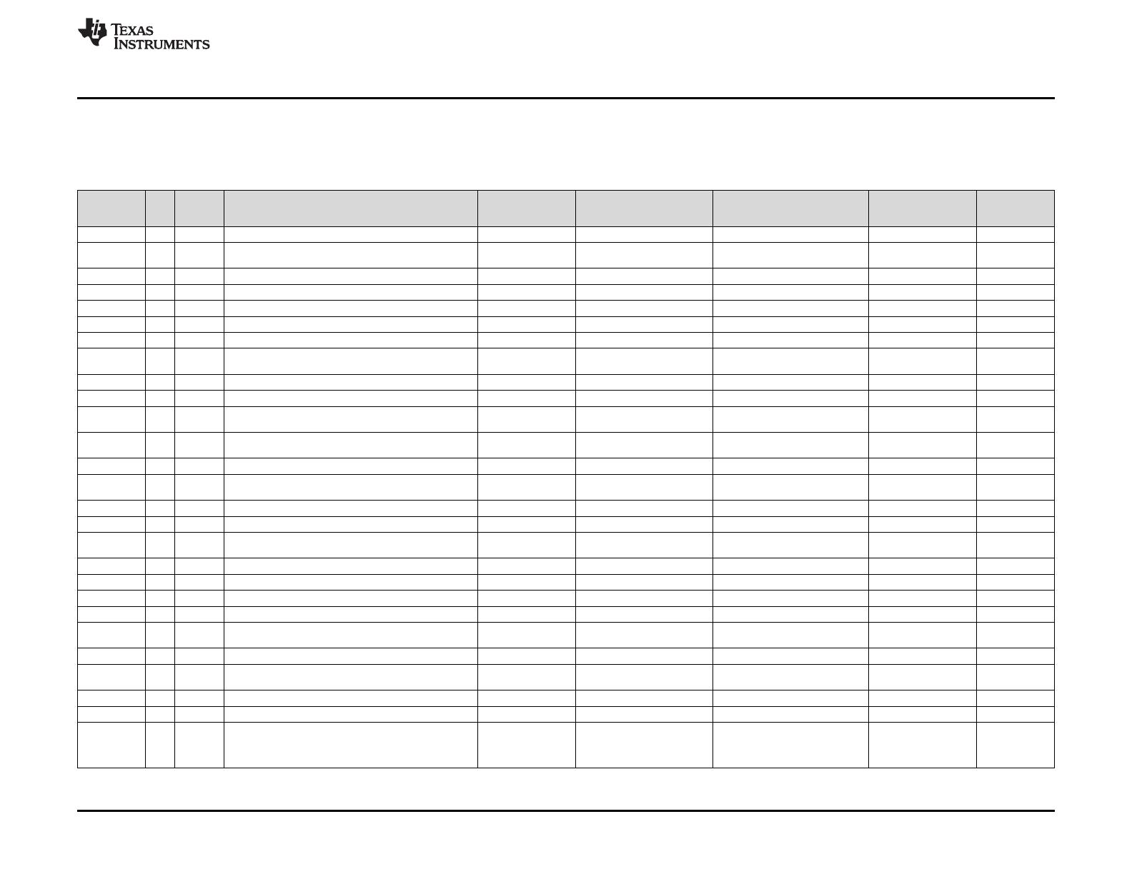
Table 2 lists the bq76200EVM BOM.
Table 2. bq76200EVM Bill of Materials
(1)
Designator QTY Value Description Package Part Number Manufacturer Alternate Alternate
Reference Part Manufacturer
Number
!PCB 1 Printed Circuit Board PWR606 Any - -
C1, C2, C3, 5 0.1uF CAP, CERM, 0.1uF, 100V, +/-10%, X7R, 0603 0603 GRM188R72A104KA35D MuRata
C4, C5
C6 1 0.47uF CAP, CERM, 0.47uF, 25V, +/-10%, X7R, 0805 0805 C2012X7R1E474K TDK
C7, C8 2 0.01uF CAP, CERM, 0.01uF, 100V, +/-10%, X7R, 0805 0805 08051C103KAT2A AVX
D1 1 75V Diode, TVS, Uni, 75V, 1500W, SMC SMC SMCJ75A Fairchild Semiconductor
D3 1 200V Diode, Ultrafast, 200V, 3A, SMC SMC ES3D-E3/57T Vishay-Semiconductor
D4 1 5.1V Diode, Zener, 5.1V, 500mW, SOD-123 SOD-123 MMSZ5231B-7-F Diodes Inc.
D5, D6, D7, 6 14V Diode, Zener, 14 V, 500 mW, SOD-123 SOD-123 MMSZ4701T1G ON Semiconductor
D8, D9, D10
H5, H6, H7, H8 4 Bumpon, Hemisphere, 0.375 X 0.235, Black Black Bumpon SJ61A2 3M
J1, J2, J4, J5 4 TERMINAL SCREW PC 30AMP, TH 12.9x6.3x7.9 mm 8199 Keystone
J3, J6 2 Header, 100mil, 2x1, Tin plated, TH Header, 2 PIN, 100mil, PEC02SAAN Sullins Connector Solutions
Tin
J7 1 Header, 100mil, 7x2, Tin plated, TH Header, 7x2, 100mil, PEC07DAAN Sullins Connector Solutions
Tin
J8 1 TERM BLOCK, 7POS, 3.5MM, TH 24.5x9.2x7.6mm 1984662 Phoenix Contact
LBL1 1 Thermal Transfer Printable Labels, 0.650" W x 0.200" H - PCB Label 0.650"H x THT-14-423-10 Brady - -
10,000 per roll 0.200"W
Q1 1 -100V MOSFET, P-CH, -100V, -0.6A, SOT-23 SOT-23 ZXMP10A13FTA Diodes Inc. None
Q3, Q4 2 100V MOSFET, N-CH, 100V, 16A, SON 5x6mm SON 5x6mm CSD19531Q5A Texas Instruments None
R1, R20, R22, 6 1.00k RES, 1.00k ohm, 1%, 0.1W, 0603 0603 CRCW06031K00FKEA Vishay-Dale
R24, R27, R29
R2, R3, R4, R5 4 1.0k RES, 1.0k ohm, 5%, 1W, 2512 2512 ERJ-1TYJ102U Panasonic
R6 1 100k RES, 100k ohm, 1%, 0.1W, 0603 0603 CRCW0603100KFKEA Vishay-Dale
R7, R8, R9 3 10.0Meg RES, 10.0Meg ohm, 1%, 0.1W, 0603 0603 CRCW060310M0FKEA Vishay-Dale
R10, R16 2 100 RES, 100 ohm, 1%, 0.1W, 0603 0603 CRCW0603100RFKEA Vishay-Dale
R11, R12, R13, 5 10.0k RES, 10.0k ohm, 1%, 0.1W, 0603 0603 CRCW060310K0FKEA Vishay-Dale
R14, R15
R17, R18, R19 3 0 RES, 0 ohm, 5%, 0.1W, 0603 0603 CRCW06030000Z0EA Vishay-Dale
R21, R23, R25, 5 39.2k RES, 39.2k ohm, 1%, 0.1W, 0603 0603 CRCW060339K2FKEA Vishay-Dale
R28, R30
R26 1 300k RES, 300k ohm, 0.1%, 0.1W, 0603 0603 RG1608P-304-B-T5 Susumu Co Ltd
R36 1 11.3k RES, 11.3k ohm, 0.1%, 0.1W, 0603 0603 RG1608P-1132-B-T5 Susumu Co Ltd
SH-J1, SH-J2, 7 1x2 Shunt, 100mil, Gold plated, Black Shunt 969102-0000-DA 3M SNT-100-BK-G Samtec
SH-J3, SH-J4,
SH-J5, SH-J6,
SH-J7
(1)
Unless otherwise noted in the Alternate Part Number and/or Alternate Manufacturer columns, all parts may be substituted with equivalents.
15
SLVU926July 2015 bq76200 High Voltage Battery Pack Front-End Charge/Discharge High-Side
NFET Driver Evaluation Module
Submit Documentation Feedback
Copyright © 2015, Texas Instruments Incorporated
Related Documentation from Texas Instruments
www.ti.com
Table 2. bq76200EVM Bill of Materials
(1)
(continued)
Designator QTY Value Description Package Part Number Manufacturer Alternate Alternate
Reference Part Manufacturer
Number
TP1, TP2, TP3, 13 SMT Test Point, Miniature, SMT Testpoint_Keystone_M 5015 Keystone
TP4, TP5, TP6, iniature
TP7, TP8, TP9,
TP10, TP11,
TP12, TP13
TP14, TP15, 4 SMT Test Point, Compact, SMT Testpoint_Keystone_C 5016 Keystone
TP16, TP17 ompact
U1 1 bq76200: Low-Power, High-Side N-channel FET Driver with PW0016A BQ76200PW Texas Instruments None
Pack Voltage Monitor, PW0016A
D2 0 75V Diode, TVS, Uni, 75V, 1500W, SMC SMC SMCJ75A Fairchild Semiconductor
FID1, FID2, 0 Fiducial mark. There is nothing to buy or mount. Fiducial N/A N/A
FID3
H1, H2, H3, H4 0 Machine Screw, Round, #4-40 x 1/4, Nylon, Philips panhead Screw NY PMS 440 0025 PH B&F Fastener Supply - -
H9 0 HEATSINK DC/DC HALF BRICK VERT DC/DC Half Brick 518-95AB Wakefield Solutions
Vertical Heat Sink
H10, H11 0 Heatsink, DDPAK/TO-263, SMT Heatsink, DDPAk 573300D00010G Aavid
Q2 0 -60V MOSFET, P-CH, -60V, -19A, DPAK DPAK SUD19P06-60L Vishay-Siliconix None
Q5, Q6 0 100V MOSFET, N-CH, 100V, 18A, DDPAK DDPAK AOB290L AOS None
Q7, Q8 0 100V MOSFET, N-CH, 100V, 97A, TO-220AB TO-220AB IRFB4410ZPBF International Rectifier None
R31, R32, R33, 0 10.0Meg RES, 10.0Meg ohm, 1%, 0.1W, 0603 0603 CRCW060310M0FKEA Vishay-Dale
R34, R35
7 Related Documentation from Texas Instruments
bq76200, High Voltage Battery Pack Front-End Charge/Discharge High-Side NFET Driver data sheet, SLUSC16
16
bq76200 High Voltage Battery Pack Front-End Charge/Discharge High-Side SLVU926July 2015
NFET Driver Evaluation Module
Submit Documentation Feedback
Copyright © 2015, Texas Instruments Incorporated
STANDARD TERMS AND CONDITIONS FOR EVALUATION MODULES
1. Delivery: TI delivers TI evaluation boards, kits, or modules, including any accompanying demonstration software, components, or
documentation (collectively, an “EVM” or “EVMs”) to the User (“User”) in accordance with the terms and conditions set forth herein.
Acceptance of the EVM is expressly subject to the following terms and conditions.
1.1 EVMs are intended solely for product or software developers for use in a research and development setting to facilitate feasibility
evaluation, experimentation, or scientific analysis of TI semiconductors products. EVMs have no direct function and are not
finished products. EVMs shall not be directly or indirectly assembled as a part or subassembly in any finished product. For
clarification, any software or software tools provided with the EVM (“Software”) shall not be subject to the terms and conditions
set forth herein but rather shall be subject to the applicable terms and conditions that accompany such Software
1.2 EVMs are not intended for consumer or household use. EVMs may not be sold, sublicensed, leased, rented, loaned, assigned,
or otherwise distributed for commercial purposes by Users, in whole or in part, or used in any finished product or production
system.
2 Limited Warranty and Related Remedies/Disclaimers:
2.1 These terms and conditions do not apply to Software. The warranty, if any, for Software is covered in the applicable Software
License Agreement.
2.2 TI warrants that the TI EVM will conform to TI's published specifications for ninety (90) days after the date TI delivers such EVM
to User. Notwithstanding the foregoing, TI shall not be liable for any defects that are caused by neglect, misuse or mistreatment
by an entity other than TI, including improper installation or testing, or for any EVMs that have been altered or modified in any
way by an entity other than TI. Moreover, TI shall not be liable for any defects that result from User's design, specifications or
instructions for such EVMs. Testing and other quality control techniques are used to the extent TI deems necessary or as
mandated by government requirements. TI does not test all parameters of each EVM.
2.3 If any EVM fails to conform to the warranty set forth above, TI's sole liability shall be at its option to repair or replace such EVM,
or credit User's account for such EVM. TI's liability under this warranty shall be limited to EVMs that are returned during the
warranty period to the address designated by TI and that are determined by TI not to conform to such warranty. If TI elects to
repair or replace such EVM, TI shall have a reasonable time to repair such EVM or provide replacements. Repaired EVMs shall
be warranted for the remainder of the original warranty period. Replaced EVMs shall be warranted for a new full ninety (90) day
warranty period.
3 Regulatory Notices:
3.1 United States
3.1.1 Notice applicable to EVMs not FCC-Approved:
This kit is designed to allow product developers to evaluate electronic components, circuitry, or software associated with the kit
to determine whether to incorporate such items in a finished product and software developers to write software applications for
use with the end product. This kit is not a finished product and when assembled may not be resold or otherwise marketed unless
all required FCC equipment authorizations are first obtained. Operation is subject to the condition that this product not cause
harmful interference to licensed radio stations and that this product accept harmful interference. Unless the assembled kit is
designed to operate under part 15, part 18 or part 95 of this chapter, the operator of the kit must operate under the authority of
an FCC license holder or must secure an experimental authorization under part 5 of this chapter.
3.1.2 For EVMs annotated as FCC FEDERAL COMMUNICATIONS COMMISSION Part 15 Compliant:
CAUTION
This device complies with part 15 of the FCC Rules. Operation is subject to the following two conditions: (1) This device may not
cause harmful interference, and (2) this device must accept any interference received, including interference that may cause
undesired operation.
Changes or modifications not expressly approved by the party responsible for compliance could void the user's authority to
operate the equipment.
FCC Interference Statement for Class A EVM devices
NOTE: This equipment has been tested and found to comply with the limits for a Class A digital device, pursuant to part 15 of
the FCC Rules. These limits are designed to provide reasonable protection against harmful interference when the equipment is
operated in a commercial environment. This equipment generates, uses, and can radiate radio frequency energy and, if not
installed and used in accordance with the instruction manual, may cause harmful interference to radio communications.
Operation of this equipment in a residential area is likely to cause harmful interference in which case the user will be required to
correct the interference at his own expense.
SPACER
SPACER
SPACER
SPACER
SPACER
SPACER
SPACER
SPACER
FCC Interference Statement for Class B EVM devices
NOTE: This equipment has been tested and found to comply with the limits for a Class B digital device, pursuant to part 15 of
the FCC Rules. These limits are designed to provide reasonable protection against harmful interference in a residential
installation. This equipment generates, uses and can radiate radio frequency energy and, if not installed and used in accordance
with the instructions, may cause harmful interference to radio communications. However, there is no guarantee that interference
will not occur in a particular installation. If this equipment does cause harmful interference to radio or television reception, which
can be determined by turning the equipment off and on, the user is encouraged to try to correct the interference by one or more
of the following measures:
Reorient or relocate the receiving antenna.
Increase the separation between the equipment and receiver.
Connect the equipment into an outlet on a circuit different from that to which the receiver is connected.
Consult the dealer or an experienced radio/TV technician for help.
3.2 Canada
3.2.1 For EVMs issued with an Industry Canada Certificate of Conformance to RSS-210
Concerning EVMs Including Radio Transmitters:
This device complies with Industry Canada license-exempt RSS standard(s). Operation is subject to the following two conditions:
(1) this device may not cause interference, and (2) this device must accept any interference, including interference that may
cause undesired operation of the device.
Concernant les EVMs avec appareils radio:
Le présent appareil est conforme aux CNR d'Industrie Canada applicables aux appareils radio exempts de licence. L'exploitation
est autorisée aux deux conditions suivantes: (1) l'appareil ne doit pas produire de brouillage, et (2) l'utilisateur de l'appareil doit
accepter tout brouillage radioélectrique subi, même si le brouillage est susceptible d'en compromettre le fonctionnement.
Concerning EVMs Including Detachable Antennas:
Under Industry Canada regulations, this radio transmitter may only operate using an antenna of a type and maximum (or lesser)
gain approved for the transmitter by Industry Canada. To reduce potential radio interference to other users, the antenna type
and its gain should be so chosen that the equivalent isotropically radiated power (e.i.r.p.) is not more than that necessary for
successful communication. This radio transmitter has been approved by Industry Canada to operate with the antenna types
listed in the user guide with the maximum permissible gain and required antenna impedance for each antenna type indicated.
Antenna types not included in this list, having a gain greater than the maximum gain indicated for that type, are strictly prohibited
for use with this device.
Concernant les EVMs avec antennes détachables
Conformément à la réglementation d'Industrie Canada, le présent émetteur radio peut fonctionner avec une antenne d'un type et
d'un gain maximal (ou inférieur) approuvé pour l'émetteur par Industrie Canada. Dans le but de réduire les risques de brouillage
radioélectrique à l'intention des autres utilisateurs, il faut choisir le type d'antenne et son gain de sorte que la puissance isotrope
rayonnée équivalente (p.i.r.e.) ne dépasse pas l'intensité nécessaire à l'établissement d'une communication satisfaisante. Le
présent émetteur radio a é approuvé par Industrie Canada pour fonctionner avec les types d'antenne énumérés dans le
manuel d’usage et ayant un gain admissible maximal et l'impédance requise pour chaque type d'antenne. Les types d'antenne
non inclus dans cette liste, ou dont le gain est supérieur au gain maximal indiqué, sont strictement interdits pour l'exploitation de
l'émetteur
3.3 Japan
3.3.1 Notice for EVMs delivered in Japan: Please see http://www.tij.co.jp/lsds/ti_ja/general/eStore/notice_01.page 日本国内に
輸入される評価用キット、ボードについては、次のところをご覧ください。
http://www.tij.co.jp/lsds/ti_ja/general/eStore/notice_01.page
3.3.2 Notice for Users of EVMs Considered “Radio Frequency Products” in Japan: EVMs entering Japan may not be certified
by TI as conforming to Technical Regulations of Radio Law of Japan.
If User uses EVMs in Japan, not certified to Technical Regulations of Radio Law of Japan, User is required by Radio Law of
Japan to follow the instructions below with respect to EVMs:
1. Use EVMs in a shielded room or any other test facility as defined in the notification #173 issued by Ministry of Internal
Affairs and Communications on March 28, 2006, based on Sub-section 1.1 of Article 6 of the Ministry’s Rule for
Enforcement of Radio Law of Japan,
2. Use EVMs only after User obtains the license of Test Radio Station as provided in Radio Law of Japan with respect to
EVMs, or
3. Use of EVMs only after User obtains the Technical Regulations Conformity Certification as provided in Radio Law of Japan
with respect to EVMs. Also, do not transfer EVMs, unless User gives the same notice above to the transferee. Please note
that if User does not follow the instructions above, User will be subject to penalties of Radio Law of Japan.
SPACER
SPACER
SPACER
SPACER
SPACER
【無線電波を送信する製品の開発キットをお使いになる際の注意事項】 開発キットの中には技術基準適合証明を受けて
いないものがあります。 技術適合証明を受けていないもののご使用に際しては、電波法遵守のため、以下のいずれかの
措置を取っていただく必要がありますのでご注意ください。
1. 電波法施行規則第6条第1項第1号に基づく平成18328日総務省告示第173号で定められた電波暗室等の試験設備でご使用
いただく。
2. 実験局の免許を取得後ご使用いただく。
3. 技術基準適合証明を取得後ご使用いただく。
なお、本製品は、上記の「ご使用にあたっての注意」を譲渡先、移転先に通知しない限り、譲渡、移転できないものとします。
上記を遵守頂けない場合は、電波法の罰則が適用される可能性があることをご留意ください。 日本テキサス・イ
ンスツルメンツ株式会社
東京都新宿区西新宿6丁目24番1号
西新宿三井ビル
3.3.3 Notice for EVMs for Power Line Communication: Please see http://www.tij.co.jp/lsds/ti_ja/general/eStore/notice_02.page
電力線搬送波通信についての開発キットをお使いになる際の注意事項については、次のところをご覧くださ
い。http://www.tij.co.jp/lsds/ti_ja/general/eStore/notice_02.page
SPACER
4 EVM Use Restrictions and Warnings:
4.1 EVMS ARE NOT FOR USE IN FUNCTIONAL SAFETY AND/OR SAFETY CRITICAL EVALUATIONS, INCLUDING BUT NOT
LIMITED TO EVALUATIONS OF LIFE SUPPORT APPLICATIONS.
4.2 User must read and apply the user guide and other available documentation provided by TI regarding the EVM prior to handling
or using the EVM, including without limitation any warning or restriction notices. The notices contain important safety information
related to, for example, temperatures and voltages.
4.3 Safety-Related Warnings and Restrictions:
4.3.1 User shall operate the EVM within TI’s recommended specifications and environmental considerations stated in the user
guide, other available documentation provided by TI, and any other applicable requirements and employ reasonable and
customary safeguards. Exceeding the specified performance ratings and specifications (including but not limited to input
and output voltage, current, power, and environmental ranges) for the EVM may cause personal injury or death, or
property damage. If there are questions concerning performance ratings and specifications, User should contact a TI
field representative prior to connecting interface electronics including input power and intended loads. Any loads applied
outside of the specified output range may also result in unintended and/or inaccurate operation and/or possible
permanent damage to the EVM and/or interface electronics. Please consult the EVM user guide prior to connecting any
load to the EVM output. If there is uncertainty as to the load specification, please contact a TI field representative.
During normal operation, even with the inputs and outputs kept within the specified allowable ranges, some circuit
components may have elevated case temperatures. These components include but are not limited to linear regulators,
switching transistors, pass transistors, current sense resistors, and heat sinks, which can be identified using the
information in the associated documentation. When working with the EVM, please be aware that the EVM may become
very warm.
4.3.2 EVMs are intended solely for use by technically qualified, professional electronics experts who are familiar with the
dangers and application risks associated with handling electrical mechanical components, systems, and subsystems.
User assumes all responsibility and liability for proper and safe handling and use of the EVM by User or its employees,
affiliates, contractors or designees. User assumes all responsibility and liability to ensure that any interfaces (electronic
and/or mechanical) between the EVM and any human body are designed with suitable isolation and means to safely
limit accessible leakage currents to minimize the risk of electrical shock hazard. User assumes all responsibility and
liability for any improper or unsafe handling or use of the EVM by User or its employees, affiliates, contractors or
designees.
4.4 User assumes all responsibility and liability to determine whether the EVM is subject to any applicable international, federal,
state, or local laws and regulations related to User’s handling and use of the EVM and, if applicable, User assumes all
responsibility and liability for compliance in all respects with such laws and regulations. User assumes all responsibility and
liability for proper disposal and recycling of the EVM consistent with all applicable international, federal, state, and local
requirements.
5. Accuracy of Information: To the extent TI provides information on the availability and function of EVMs, TI attempts to be as accurate
as possible. However, TI does not warrant the accuracy of EVM descriptions, EVM availability or other information on its websites as
accurate, complete, reliable, current, or error-free.
SPACER
SPACER
SPACER
SPACER
SPACER
SPACER
SPACER
6. Disclaimers:
6.1 EXCEPT AS SET FORTH ABOVE, EVMS AND ANY WRITTEN DESIGN MATERIALS PROVIDED WITH THE EVM (AND THE
DESIGN OF THE EVM ITSELF) ARE PROVIDED "AS IS" AND "WITH ALL FAULTS." TI DISCLAIMS ALL OTHER
WARRANTIES, EXPRESS OR IMPLIED, REGARDING SUCH ITEMS, INCLUDING BUT NOT LIMITED TO ANY IMPLIED
WARRANTIES OF MERCHANTABILITY OR FITNESS FOR A PARTICULAR PURPOSE OR NON-INFRINGEMENT OF ANY
THIRD PARTY PATENTS, COPYRIGHTS, TRADE SECRETS OR OTHER INTELLECTUAL PROPERTY RIGHTS.
6.2 EXCEPT FOR THE LIMITED RIGHT TO USE THE EVM SET FORTH HEREIN, NOTHING IN THESE TERMS AND
CONDITIONS SHALL BE CONSTRUED AS GRANTING OR CONFERRING ANY RIGHTS BY LICENSE, PATENT, OR ANY
OTHER INDUSTRIAL OR INTELLECTUAL PROPERTY RIGHT OF TI, ITS SUPPLIERS/LICENSORS OR ANY OTHER THIRD
PARTY, TO USE THE EVM IN ANY FINISHED END-USER OR READY-TO-USE FINAL PRODUCT, OR FOR ANY
INVENTION, DISCOVERY OR IMPROVEMENT MADE, CONCEIVED OR ACQUIRED PRIOR TO OR AFTER DELIVERY OF
THE EVM.
7. USER'S INDEMNITY OBLIGATIONS AND REPRESENTATIONS. USER WILL DEFEND, INDEMNIFY AND HOLD TI, ITS
LICENSORS AND THEIR REPRESENTATIVES HARMLESS FROM AND AGAINST ANY AND ALL CLAIMS, DAMAGES, LOSSES,
EXPENSES, COSTS AND LIABILITIES (COLLECTIVELY, "CLAIMS") ARISING OUT OF OR IN CONNECTION WITH ANY
HANDLING OR USE OF THE EVM THAT IS NOT IN ACCORDANCE WITH THESE TERMS AND CONDITIONS. THIS OBLIGATION
SHALL APPLY WHETHER CLAIMS ARISE UNDER STATUTE, REGULATION, OR THE LAW OF TORT, CONTRACT OR ANY
OTHER LEGAL THEORY, AND EVEN IF THE EVM FAILS TO PERFORM AS DESCRIBED OR EXPECTED.
8. Limitations on Damages and Liability:
8.1 General Limitations. IN NO EVENT SHALL TI BE LIABLE FOR ANY SPECIAL, COLLATERAL, INDIRECT, PUNITIVE,
INCIDENTAL, CONSEQUENTIAL, OR EXEMPLARY DAMAGES IN CONNECTION WITH OR ARISING OUT OF THESE
TERMS ANDCONDITIONS OR THE USE OF THE EVMS PROVIDED HEREUNDER, REGARDLESS OF WHETHER TI HAS
BEEN ADVISED OF THE POSSIBILITY OF SUCH DAMAGES. EXCLUDED DAMAGES INCLUDE, BUT ARE NOT LIMITED
TO, COST OF REMOVAL OR REINSTALLATION, ANCILLARY COSTS TO THE PROCUREMENT OF SUBSTITUTE GOODS
OR SERVICES, RETESTING, OUTSIDE COMPUTER TIME, LABOR COSTS, LOSS OF GOODWILL, LOSS OF PROFITS,
LOSS OF SAVINGS, LOSS OF USE, LOSS OF DATA, OR BUSINESS INTERRUPTION. NO CLAIM, SUIT OR ACTION SHALL
BE BROUGHT AGAINST TI MORE THAN ONE YEAR AFTER THE RELATED CAUSE OF ACTION HAS OCCURRED.
8.2 Specific Limitations. IN NO EVENT SHALL TI'S AGGREGATE LIABILITY FROM ANY WARRANTY OR OTHER OBLIGATION
ARISING OUT OF OR IN CONNECTION WITH THESE TERMS AND CONDITIONS, OR ANY USE OF ANY TI EVM
PROVIDED HEREUNDER, EXCEED THE TOTAL AMOUNT PAID TO TI FOR THE PARTICULAR UNITS SOLD UNDER
THESE TERMS AND CONDITIONS WITH RESPECT TO WHICH LOSSES OR DAMAGES ARE CLAIMED. THE EXISTENCE
OF MORE THAN ONE CLAIM AGAINST THE PARTICULAR UNITS SOLD TO USER UNDER THESE TERMS AND
CONDITIONS SHALL NOT ENLARGE OR EXTEND THIS LIMIT.
9. Return Policy. Except as otherwise provided, TI does not offer any refunds, returns, or exchanges. Furthermore, no return of EVM(s)
will be accepted if the package has been opened and no return of the EVM(s) will be accepted if they are damaged or otherwise not in
a resalable condition. If User feels it has been incorrectly charged for the EVM(s) it ordered or that delivery violates the applicable
order, User should contact TI. All refunds will be made in full within thirty (30) working days from the return of the components(s),
excluding any postage or packaging costs.
10. Governing Law: These terms and conditions shall be governed by and interpreted in accordance with the laws of the State of Texas,
without reference to conflict-of-laws principles. User agrees that non-exclusive jurisdiction for any dispute arising out of or relating to
these terms and conditions lies within courts located in the State of Texas and consents to venue in Dallas County, Texas.
Notwithstanding the foregoing, any judgment may be enforced in any United States or foreign court, and TI may seek injunctive relief
in any United States or foreign court.
Mailing Address: Texas Instruments, Post Office Box 655303, Dallas, Texas 75265
Copyright © 2015, Texas Instruments Incorporated
spacer
  • Page 1 1
  • Page 2 2
  • Page 3 3
  • Page 4 4
  • Page 5 5
  • Page 6 6
  • Page 7 7
  • Page 8 8
  • Page 9 9
  • Page 10 10
  • Page 11 11
  • Page 12 12
  • Page 13 13
  • Page 14 14
  • Page 15 15
  • Page 16 16
  • Page 17 17
  • Page 18 18
  • Page 19 19
  • Page 20 20
  • Page 21 21

Texas Instruments bq76200EVM User guide

Type
User guide

Ask a question and I''ll find the answer in the document

Finding information in a document is now easier with AI