
PROTECTION PRODUCTS
1
www.semtech.com
PRELIMINARY
PROTECTION PRODUCTS
SD05C through SD24C
Single Line TVS Diode for ESD
Protection in Portable Electronics
Description
Features
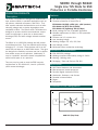
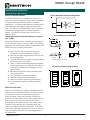
Schematic & PIN Configuration
Revision 07/06/04
Applications
Mechanical Characteristics
The SDxxC TVS diodes are designed to replace multi-
layer varistors (MLVs) in portable applications such as
cell phones, notebook computers, and PDA’s. They
offer superior electrical characteristics such as lower
clamping voltage and no device degradation when
compared to MLVs. The SDxxC series TVS diodes are
designed to protect sensitive semiconductor compo-
nents from damage or upset due to electrostatic
discharge (ESD) and other voltage induced transient
events.
The SDxxC is in a SOD-323 package and will protect
one bidirectional line. They are available with working
voltages of 5 - 24 volts. These devices will fit on the
same PCB pad area as an 0805 MLV device. They give
the designer the flexibility to protect one line in applica-
tions where arrays are not practical. Additionally, it
may be “sprinkled” around the board in applications
where board space is at a premium.
They may may be used to meet the ESD immunity
requirements of IEC 61000-4-2, Level 4 (±15kV air,
±8kV contact discharge).
350 Watts peak pulse power (t
p
= 8/20µs)
Transient protection for data lines to
IEC 61000-4-2 (ESD) ±15kV (air), ±8kV (contact)
IEC 61000-4-4 (EFT) 40A (5/50ns)
IEC 61000-4-5 (Lightning) 24A (8/20µs)
Small package for use in portable electronics
Suitable replacement for MLV’s in ESD protection
applications
Protects one I/O or power line
Low clamping voltage
Working voltages: 5V, 12V, 15V, 24V
Low leakage current
Solid-state silicon avalanche technology
EIAJ SOD-323 package
Molding compound flammability rating: UL 94V-0
Marking : Marking code
Packaging : Tape and Reel per EIA 481
Cell Phone Handsets and Accessories
Microprocessor based equipment
Personal Digital Assistants (PDA’s)
Notebooks, Desktops, and Servers
Portable Instrumentation
Pagers
Peripherals
SOD-323 (Top View)
12

2 2004 Semtech Corp.
www.semtech.com
PROTECTION PRODUCTS
SD05C through SD24C
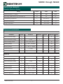
Absolute Maximum Rating
Electrical Characteristics
SVTC50DS
retemaraPlobmySsnoitidnoCmuminiMlacipyTmumixaMstinU
egatloVffO-dnatSesreveRV
MWR
5V
egatloVnwodkaerBesreveRV
RB
I
t
Am1=6 V
tnerruCegakaeLesreveRI
R
V
MWR
C°52=T,V5=01Aµ
egatloVgnipmalCV
C
I
PP
t,A5=
p
sµ02/8=8.9V
egatloVgnipmalCV
C
I
PP
t,A42=
p
sµ02/8=5.41V
tnerruCesluPkaePI
PP
t
p
sµ02/8=42A
ecnaticapaCnoitcnuJC
j
V
R
zHM1=f,V0=002Fp
SVTC21DS
retemaraPlobmySsnoitidnoCmuminiMlacipyTmumixaMstinU
egatloVffO-dnatSesreveRV
MWR
21V
egatloVnwodkaerBesreveRV
RB
I
t
Am1=3.31V
tnerruCegakaeLesreveRI
R
V
MWR
C°52=T,V21=1Aµ
egatloVgnipmalCV
C
I
PP
t,A5=
p
sµ02/8=91V
egatloVgnipmalCV
C
I
PP
t,A51=
p
sµ02/8=42V
tnerruCesluPkaePI
PP
t
p
sµ02/8=51A
ecnaticapaCnoitcnuJC
j
V
R
zHM1=f,V0=001Fp
gnitaRlobmySeulaVstinU
t(rewoPesluPkaeP
p
)sµ02/8=P
kp
053sttaW
)2-4-00016CEIrepmrofevaWMBH(egatloVDSEV
DSE
03Vk
erutarepmeTgniredloSdaeLT
L
).ces01(062C°
erutarepmeTgnitarepOT
J
521+ot55-C°
erutarepmeTegarotST
GTS
051+ot55-C°

3 2004 Semtech Corp.
www.semtech.com
PRELIMINARY
PROTECTION PRODUCTS
SD05C through SD24C
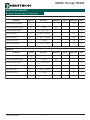
Electrical Characteristics (Continued)
SVTC51DS
retemaraPlobmySsnoitidnoCmuminiMlacipyTmumixaMstinU
egatloVffO-dnatSesreveRV
MWR
51V
egatloVnwodkaerBesreveRV
RB
I
t
Am1=7.61V
tnerruCegakaeLesreveRI
R
V
MWR
C°52=T,V51=1Aµ
egatloVgnipmalCV
C
I
PP
t,A5=
p
sµ02/8=42V
egatloVgnipmalCV
C
I
PP
t,A21=
p
sµ02/8=92V
tnerruCesluPkaePI
PP
t
p
sµ02/8=21A
ecnaticapaCnoitcnuJC
j
V
R
zHM1=f,V0=57Fp
SVTC42DS
retemaraPlobmySsnoitidnoCmuminiMlacipyTmumixaMstinU
egatloVffO-dnatSesreveRV
MWR
42V
egatloVnwodkaerBesreveRV
RB
I
t
Am1=7.62V
tnerruCegakaeLesreveRI
R
V
MWR
C°52=T,V42=1Aµ
egatloVgnipmalCV
C
I
PP
t,A5=
p
sµ02/8=04V
egatloVgnipmalCV
C
I
PP
t,A8=
p
sµ02/8=44V
tnerruCesluPkaePI
PP
t
p
sµ02/8=8A
ecnaticapaCnoitcnuJC
j
V
R
zHM1=f,V0=05Fp

4 2004 Semtech Corp.
www.semtech.com
PROTECTION PRODUCTS
SD05C through SD24C
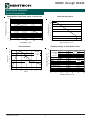
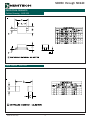
Typical Characteristics
Non-Repetitive Peak Pulse Power vs. Pulse Time Power Derating Curve
0
10
20
30
40
50
60
70
80
90
100
110
0 25 50 75 100 125 150
Ambient Temperature - T
A
(
o
C)
% of Rated Power or I
PP
Clamping Voltage vs. Peak Pulse Current
0
10
20
30
40
50
60
70
80
90
100
110
0 5 10 15 20 25 30
Time (µs)
Percent of I
PP
e
-t
td = I
PP
/2
Waveform
Parameters:
tr = 8µs
td = 20µs
Pulse Waveform
0.01
0.1
1
10
0.1 1 10 100 1000
Pulse Duration - t
p
(µs)
Peak Pulse Power - P
pk
(kW)
0
5
10
15
20
25
30
0 5 10 15 20 25 30
Peak Pulse Current - I
PP
(A)
Clamping Voltage - V
C
(V)
Waveform
Parameters:
tr = 8µs
td = 20µs
SD05
C
SD12C

5 2004 Semtech Corp.
www.semtech.com
PRELIMINARY
PROTECTION PRODUCTS
SD05C through SD24C
Device Connection Options
The SDxxC TVS diodes are designed to protect one
data, I/O, or power supply line. The device is designed
to replace multi-layer varistors (MLVs) in portable
applications. It is easily implemented on existing 0805
MLV pads and is only slightly larger than 0603 MLV
pads. The device is bidirectional and may be used on
lines where the signal polarity is above and below
ground. The device is symmetrical, so there is no
cathode band.
Circuit Board Layout Recommendations for Suppres-
sion of ESD.
Good circuit board layout is critical for the suppression
of fast rise-time transients such as ESD. The following
guidelines are recommended (Refer to application note
SI99-01 for more detailed information):
z Place the TVS near the input terminals or
connectors to restrict transient coupling.
z Minimize the path length between the TVS and
the protected line.
z The ESD transient return path to ground should
be kept as short as possible.
z Place a TVS and decoupling capacitor between
power and ground of components that may be
vulnerable to electrostatic discharges to the
ground plane.
z Minimize all conductive loops including power
and ground loops.
z Use multilayer boards when possible.
z Minimize interconnecting line lengths
z Never run critical signals near board edges.
z Fill unused portions of the PCB with ground
plane.
Matte Tin Lead Finish
Matte tin has become the industry standard lead-free
replacement for SnPb lead finishes. A matte tin finish
is composed of 100% tin solder with large grains.
Since the solder volume on the leads is small com-
pared to the solder paste volume that is placed on the
land pattern of the PCB, the reflow profile will be
determined by the requirements of the solder paste.
Therefore, these devices are compatible with both
lead-free and SnPb assembly techniques. In addition,
unlike other lead-free compositions, matte tin does not
have any added alloys that can cause degradation of
the solder joint.
Device Schematic and Pin Configuration
Size Comparison to 0805 MLV
SOD-323 0805 MLV
Note: Nominal dimensions in inches
Component Placement Comparison
0805 MLV on SOD-323 on 0805
MLV Pad
SOD-323 on Recommended
(SOD-323) Solder Pad0805 Solder Pad
Applications Information

6 2004 Semtech Corp.
www.semtech.com
PROTECTION PRODUCTS
SD05C through SD24C
Land Pattern - SOD-323
Outline Drawing - SOD-323

7 2004 Semtech Corp.
www.semtech.com
PRELIMINARY
PROTECTION PRODUCTS
SD05C through SD24C
Contact Information
Semtech Corporation
Protection Products Division
200 Flynn Rd., Camarillo, CA 93012
Phone: (805)498-2111 FAX (805)498-3804
traP
rebmuN
hsiniFdaeL
repytQ
leeR
eziSleeR
CT.C50DSbPnS000,3”7
CT.C21DSbPnS000,3”7
CT.C51DSbPnS000,3”7
CT.C42DSbPnS000,3”7
TCT.C50DSeerfbP000,3”7
TCT.C21DSeerfbP000,3”7
TCT.C51DSeerfbP000,3”7
TCT.C42DSeerfbP000,3”7
Marking Codes
Ordering Information
Part Number
Marking
Code
SD05C
SD12C
SD15C
SD24C
5/
5
6/
6
7/
7
8/
8
-
 1
1
-
 2
2
-
 3
3
-
 4
4
-
 5
5
-
 6
6
-
 7
7


