Fujifilm P4X-0028-2M-800 Datasheet
- Category
- Processors
- Type
- Datasheet
This manual is also suitable for

Low Voltage Intel
®
Xeon™ Processor
with 800 MHz System Bus
Datasheet
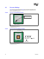
Product Features
The Low Voltage Intel
®
Xeon™ processor with 800 MHz system bus is designed for
high-performance dual-processor applications. Based on the Intel NetBurst
®
microarchitecture
and the Hyper-Threading Technology, it is binary compatible with previous Intel
®
Architecture
(IA-32) processors. The Low Voltage Intel Xeon processor with 800 MHz system bus is scalable
to two processors in a multiprocessor system providing exceptional performance for applications
running on advanced operating systems such as Windows XP*, Windows Server* 2003, Linux*,
and UNIX*.
■ Available at 2.80 GHz
■ 90 nm process technology
■ Dual processing support
■ Binary compatible with applications
running on previous members of Intel’s
IA-32 microprocessor line
■ Intel NetBurst
®
microarchitecture
■ Hyper-Threading Technology
■ Supports Execute Disable Bit capability
■ Hardware support for multithreaded
applications
■ Faster 800 MHz system bus
■ Rapid Execution Engine: Arithmetic Logic
Units (ALUs) run at twice the processor
core frequency
■ Hyper-Pipelined Technology
■ Advanced Dynamic Execution
■ Very deep out-of-order execution
■ Enhanced branch prediction
■ Includes 16-KB Level 1 data cache
■ Intel
®
Extended Memory 64 Technology
■ 1-MB Advanced Transfer Cache (On-die,
full speed Level 2 (L2) Cache) with 8-way
associativity and Error Correcting Code
(ECC)
■ Enables system support of up to 64 GB of
physical memory
■ 144 Streaming SIMD Extensions 2 (SSE2)
instructions
■ 13 Streaming SIMD Extensions 3 (SSE3)
instructions
■ Enhanced floating-point and multimedia
unit for enhanced video, audio, encryption,
and 3D performance
■ System Management mode
■ Thermal Monitor
■ Machine Check Architecture (MCA)
Document Number: 304097-001US
October 2004
The Low Voltage Intel Xeon processor with 800 MHz
system bus delivers compute power at unparalleled value
and flexibility for powerful workstations, internet
infrastructure, and departmental server applications. The
Intel NetBurst
®
microarchitecture and Hyper-Threading
Technology deliver outstanding performance and
headroom for peak internet server workloads, resulting in
faster response times, support for more users, and
improved scalability.

2 Datasheet
INFORMATION IN THIS DOCUMENT IS PROVIDED IN CONNECTION WITH INTEL® PRODUCTS. NO LICENSE, EXPRESS OR IMPLIED, BY
ESTOPPEL OR OTHERWISE, TO ANY INTELLECTUAL PROPERTY RIGHTS IS GRANTED BY THIS DOCUMENT. EXCEPT AS PROVIDED IN
INTEL'S TERMS AND CONDITIONS OF SALE FOR SUCH PRODUCTS, INTEL ASSUMES NO LIABILITY WHATSOEVER, AND INTEL DISCLAIMS
ANY EXPRESS OR IMPLIED WARRANTY, RELATING TO SALE AND/OR USE OF INTEL PRODUCTS INCLUDING LIABILITY OR WARRANTIES
RELATING TO FITNESS FOR A PARTICULAR PURPOSE, MERCHANTABILITY, OR INFRINGEMENT OF ANY PATENT, COPYRIGHT OR OTHER
INTELLECTUAL PROPERTY RIGHT. Intel products are not intended for use in medical, life saving, life sustaining applications.
Intel may make changes to specifications and product descriptions at any time, without notice.
Designers must not rely on the absence or characteristics of any features or instructions marked “reserved” or “undefined.” Intel reserves these for
future definition and shall have no responsibility whatsoever for conflicts or incompatibilities arising from future changes to them.
The Low Voltage Intel
®
Xeon™ processor with 800 MHz system bus may contain design defects or errors known as errata which may cause the
product to deviate from published specifications. Current characterized errata are available on request.
Hyper-Threading Technology requires a computer system with an Intel
®
Pentium
®
4 processor supporting HT Technology and a HT Technology
enabled chipset, BIOS and operating system. Performance will vary depending on the specific hardware and software you use. See Hyper-Threading
Technology (http://developer.intel.com/products/ht/Hyperthreading_more.htm) for more information.
Contact your local Intel sales office or your distributor to obtain the latest specifications and before placing your product order.
Copies of documents which have an ordering number and are referenced in this document, or other Intel literature may be obtained by calling
1-800-548-4725 or by visiting Intel's website at http://www.intel.com.
Intel, Pentium, Intel Xeon, Intel Inside, Intel NetBurst and Itanium are trademarks or registered trademarks of Intel Corporation or its subsidiaries in the
United States and other countries.
Intel
®
Extended Memory 64 Technology (Intel
®
EM64T) requires a computer system with a processor, chipset, BIOS, OS, device drivers and
applications enabled for Intel EM64T. Processor will not operate (including 32-bit operation) without an Intel EM64T-enabled BIOS. Performance will
vary depending on your hardware and software configurations. Intel EM64T-enabled OS, BIOS, device drivers and applications may not be available.
Check with your vendor for more information.
∆
Intel processor numbers are not a measure of performance. Processor numbers differentiate features within each processor family, not across
different processor families. See http://www.intel.com/products/processor_number for details.
* Other names and brands may be claimed as the property of others.
Copyright © 2004, Intel Corporation

Datasheet 3
Contents
1.0 Introduction....................................................................................................................................9
1.1 Terminology........................................................................................................................10
1.2 References .........................................................................................................................12
1.3 State of Data.......................................................................................................................12
2.0 Electrical Specifications .............................................................................................................13
2.1 Power and Ground Pins......................................................................................................13
2.2 Decoupling Guidelines........................................................................................................13
2.2.1 V
CC
Decoupling .....................................................................................................13
2.2.2 VTT
Decoupling .....................................................................................................13
2.2.3 Front Side Bus AGTL+ Decoupling........................................................................14
2.3 Front Side Bus Clock (BCLK[1:0]) and Processor Clocking ...............................................14
2.3.1 Front Side Bus Frequency Select Signals (BSEL[1:0])..........................................14
2.3.2 Phase Lock Loop (PLL) and Filter .........................................................................15
2.4 Voltage Identification (VID).................................................................................................16
2.5 Reserved or Unused Pins...................................................................................................18
2.6 Front Side Bus Signal Groups ............................................................................................19
2.7 GTL+ Asynchronous and AGTL+ Asynchronous Signals...................................................22
2.8 Test Access Port (TAP) Connection...................................................................................22
2.9 Mixing Processors ..............................................................................................................22
2.10 Absolute Maximum and Minimum Ratings .........................................................................23
2.11 Processor DC Specifications..............................................................................................24
2.11.1 VCC Overshoot Specification................................................................................30
2.11.2 Die Voltage Validation ...........................................................................................31
3.0 Mechanical Specifications..........................................................................................................35
3.1 Package Mechanical Drawings...........................................................................................35
3.2 Processor Component Keepout Zones...............................................................................38
3.3 Package Loading Specifications.........................................................................................38
3.4 Package Handling Guidelines.............................................................................................39
3.5 Package Insertion Specifications........................................................................................39
3.6 Processor Mass Specifications...........................................................................................39
3.7 Processor Materials............................................................................................................39
3.8 Processor Markings............................................................................................................40
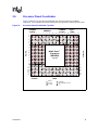
3.9 Processor Pinout Coordinates............................................................................................41
4.0 Signal Definitions .......................................................................................................................43
4.1 Signal Definitions................................................................................................................43
5.0 Pin List..........................................................................................................................................53
5.1 Low Voltage Intel
®
Xeon™ Processor with 800 MHz System Bus Pin Assignments.........53
5.1.1 Pin Listing by Pin Name.........................................................................................54
5.1.2 Pin Listing by Pin Number .....................................................................................62
6.0 Thermal Specifications ..............................................................................................................71
6.1 Package Thermal Specifications ........................................................................................71
6.1.1 Thermal Specifications ..........................................................................................71

4 Datasheet
6.1.2 Thermal Metrology.................................................................................................74
6.2 Processor Thermal Features..............................................................................................74
6.2.1 Thermal Monitor.....................................................................................................74
6.2.2 On-Demand Mode.................................................................................................75
6.2.3 PROCHOT# Signal Pin..........................................................................................75
6.2.4 FORCEPR# Signal Pin..........................................................................................75
6.2.5 THERMTRIP# Signal Pin.......................................................................................76
6.2.6 TCONTROL and Fan Speed Reduction................................................................76
6.2.7 Thermal Diode.......................................................................................................76
7.0 Features........................................................................................................................................79
7.1 Power-On Configuration Options........................................................................................79
7.2 Clock Control and Low Power States.................................................................................79
7.2.1 Normal State..........................................................................................................80
7.2.2 HALT Power-Down State.......................................................................................80
7.2.3 Stop-Grant State....................................................................................................82
7.2.4 HALT Snoop State or Snoop State........................................................................82
7.2.5 Sleep State............................................................................................................83
8.0 Debug Tools Specifications .......................................................................................................85
8.1 Debug Port System Requirements.....................................................................................85
8.2 Target System Implementation...........................................................................................85
8.2.1 System Implementation.........................................................................................85
8.3 Logic Analyzer Interface (LAI)...........................................................................................85
8.3.1 Mechanical Considerations....................................................................................86
8.3.2 Electrical Considerations.......................................................................................86

Datasheet 5
Figures
1 Phase Lock Loop (PLL) Filter Requirements .............................................................................15
2 Low Voltage Intel
®
Xeon™ Processor with 800 MHz System Bus Load Current vs.
Time (VRM 10.0)........................................................................................................................27
3 VCC Static and Transient Tolerance..........................................................................................29
4 VCC Overshoot Example Waveform..........................................................................................30
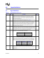
5 Processor Package Assembly Sketch........................................................................................35
6 Processor Package Drawing (Sheet 1 of 2)...............................................................................36
7 Processor Package Drawing (Sheet 2 of 2)...............................................................................37
8 Processor Top-Side Markings (Example)...................................................................................40
9 Processor Bottom-Side Markings (Example) .............................................................................40
10 Processor Pinout Coordinates, Top View...................................................................................41
11 Processor Pinout Coordinates, Bottom View .............................................................................42
12 Low Voltage Intel
®
Xeon™ Processor with 800 MHz System Bus Thermal Profile...................73
13 Case Temperature (TCASE) Measurement Location ................................................................74
14 Stop Clock State Machine..........................................................................................................81

6 Datasheet
Tables
1 Features of the Low Voltage Intel
®
Xeon™ Processor with 800 MHz System Bus .....................9
2 Core Frequency to Front Side Bus Multiplier Configuration.......................................................14
3 BSEL[1:0] Frequency Table.......................................................................................................15
4 Voltage Identification Definition..................................................................................................17
5 Front Side Bus Signal Groups....................................................................................................20
6 Signal Description Table ............................................................................................................21
7 Signal Reference Voltages.........................................................................................................21
8 Absolute Maximum and Minimum Ratings.................................................................................23
9 Voltage and Current Specifications............................................................................................25
10 VCC Static and Transient Tolerance..........................................................................................28
11 VCC Overshoot Specifications...................................................................................................30
12 BSEL[1:0] and VID[5:0] Signal Group DC Specifications...........................................................31
13 AGTL+ Signal Group DC Specifications ....................................................................................31
14 PWRGOOD Input and TAP Signal Group DC Specifications.....................................................32
15 GTL+ Asynchronous and AGTL+ Asynchronous Signal Group DC Specifications....................32
16 VIDPWRGD DC Specifications..................................................................................................33
17 Processor Loading Specifications..............................................................................................38
18 Package Handling Guidelines....................................................................................................39
19 Processor Materials ...................................................................................................................39
20 Signal Definitions .......................................................................................................................43
21 Pin Listing by Pin Name.............................................................................................................54
22 Pin Listing by Pin Number..........................................................................................................62
23 Low Voltage Intel
®
Xeon™ Processor with 800 MHz System Bus Thermal Specifications.......72
24 Low Voltage Intel
®
Xeon™ Processor with 800 MHz System Bus Thermal Profile...................73
25 Thermal Diode Parameters........................................................................................................76
26 Thermal Diode Interface.............................................................................................................77
27 Power-On Configuration Option Pins.........................................................................................79

Datasheet 7
Revision History
Date Revision Description
October 2004 001 Initial release

8 Datasheet
THIS PAGE INTENTIONALLY LEFT BLANK

Datasheet 9
1.0 Introduction
The Low Voltage Intel
®
Xeon™ processor with 800 MHz system bus is a 32-bit processor based
on improvements to the Intel NetBurst
®
microarchitecture. It maintains the tradition of
compatibility with IA-32 software and includes features found in the Low-Voltage Intel
®
Xeon™
processor such as Hyper-Pipelined Technology, a Rapid Execution Engine, and an Execution Trace
Cache. Hyper-Pipelined Technology includes a multi-stage pipeline, allowing the processor to
reach much higher core frequencies. The 800 MHz system bus is a quad-pumped bus running off a
200 MHz system clock making 6.4 GB per second data transfer rates possible. The Execution
Trace Cache is a level 1 cache that stores decoded micro-operations, which removes the decoder
from the main execution path, thereby increasing performance.
The Low Voltage Intel Xeon processor with 800 MHz system bus supports Hyper-Threading
Technology. This feature allows a single, physical processor to function as two logical processors.
While some execution resources such as caches, execution units, and buses are shared, each logical
processor has its own architecture state with its own set of general-purpose registers, control
registers to provide increased system responsiveness in multitasking environments, and headroom
for next generation multi-threaded applications. More information on Hyper-Threading
Technology can be found at http://www.intel.com/technology/hyperthread.
Other features within the Intel NetBurst
®
microarchitecture include Advanced Dynamic Execution,
Advanced Transfer Cache, enhanced floating-point and multi-media unit, Streaming SIMD
Extensions 2 (SSE2) and Streaming SIMD Extensions 3 (SSE3). Advanced Dynamic Execution
improves speculative execution and branch prediction internal to the processor. The Advanced
Transfer Cache is a 1 MB, on-die, level 2 (L2) cache with increased bandwidth. The floating-point
and multi-media units include 128-bit wide registers and a separate register for data movement.
Streaming SIMD2 (SSE2) instructions provide highly efficient double-precision floating-point,
SIMD integer, and memory management operations. In addition, (SSE3) instructions have been
added to further extend the capabilities of Intel
®
processor technology. Other processor
enhancements include core frequency improvements and microarchitectural improvements.
The Low Voltage Intel Xeon processor with 800 MHz system bus supports Intel
®
Extended
Memory 64 Technology (Intel
®
EM64T) as an enhancement to Intel’s IA-32 architecture. This
enhancement allows the processor to execute operating systems and applications written to take
advantage of the 64-bit extension technology. Further details on Intel
®
Extended Memory 64
Technology and its programming model can be found in the 64-bit Extension Technology Software
Developer's Guide at http://developer.intel.com/technology/64bitextensions.
The Low Voltage Intel Xeon processor with 800 MHz system bus is intended for high performance
systems with up to two processors on one system bus. The processor will be packaged in a 604-pin
Flip Chip Micro Pin Grid Array (FC-mPGA4) package and will use a surface mount Zero Insertion
Force (ZIF) socket (mPGA604).
Table 1. Features of the Low Voltage Intel
®
Xeon™ Processor with 800 MHz System Bus
No. of Supported
Symmetric
Agents
L2 Advanced
Transfer
Cache
Front Side Bus
Frequency
Package
Low Voltage Intel
®
Xeon™
processor with 800 MHz system
bus
1–2 1 MB 800 MHz
604-pin
FC-mPGA4

10 Datasheet
Platforms based on the Low Voltage Intel
®
Xeon™ processor with 800 MHz system bus
implement independent power planes for each system bus agent. As a result, the processor core
voltage (V
CC
) and system bus termination voltage (V
TT
) must connect to separate supplies. The
processor core voltage uses power delivery guidelines denoted by VRM 10.0 and the associated
load line (see Voltage Regulator Module (VRM) and Enterprise Voltage Regulator-Down (EVRD)
10.0 Design Guidelines for further details).
The Low Voltage Intel Xeon processor with 800 MHz system bus uses a scalable system bus
protocol referred to as the “system bus” in this document. The system bus uses a split-transaction,
deferred reply protocol. The system bus uses Source-Synchronous Transfer (SST) of address and
data to improve performance. The processor transfers data four times per bus clock (4X data
transfer rate, as in AGP 4X). Along with the 4X data bus, the address bus can deliver addresses two
times per bus clock and is referred to as a ‘double-clocked’ or the 2X address bus. In addition, the
Request Phase completes in one clock cycle. Working together, the 4X data bus and 2X address bus
provide a data bus bandwidth of up to 6.4 GBytes/second (6400 MBytes/second). Finally, the
system bus is also used to deliver interrupts.
The Low Voltage Intel Xeon processor with 800 MHz system bus also includes the Execute
Disable Bit capability previously available in Itanium
®
processors. This feature combined with a
supported operating system allows memory to be marked as executable or non-executable. When
code attempts to run in non-executable memory, the processor raises an error to the operating
system. This feature can prevent some classes of viruses or worms that exploit buffer overrun
vulnerabilities and can thus help improve the overall security of the system. See the Intel
®
Architecture Software Developer’s Manual for more detailed information.
1.1 Terminology
A ‘#’ symbol after a signal name refers to an active low signal, indicating a signal is in the asserted
state when driven to a low level. For example, when RESET# is low, a reset has been requested.
Conversely, when NMI is high, a nonmaskable interrupt has occurred. In the case of signals where
the name does not imply an active state but describes part of a binary sequence (such as address or
data), the ‘#’ symbol implies that the signal is inverted. For example, D[3:0] = ‘HLHL’ refers to a
hex ‘A’, and D[3:0]# = ‘LHLH’ also refers to a hex ‘A’ (H= High logic level, L= Low logic level).
“Front side bus” or “System bus” refers to the interface between the processor, system core logic
(also known as the chipset components), and other bus agents. The system bus is a multiprocessing
interface to processors, memory, and I/O. For this document, “front side bus” or “system bus” are
used as generic terms for the “Low Voltage Intel
®
Xeon™ processor with 800 MHz system bus”.
Commonly used terms are explained here for clarification:
• Low Voltage Intel
®
Xeon™ Processor with 800 MHz System Bus — Intel
®
32-bit
microprocessor intended for single/dual-processor applications. The Low Voltage Intel
®
Xeon™ processor with 800 MHz system bus is based on Intel’s 90 nm process and will
include core frequency improvements, a large cache array, microarchitectural improvements
and additional instructions. The Low Voltage Intel Xeon processor with 800 MHz system bus
will use the mPGA604 socket. For this document, “processor” is used as the generic term for
the “Low Voltage Intel
®
Xeon™ processor with 800 MHz system bus”.
• Central Agent — The central agent is the host bridge to the processor and is typically known
as the chipset.

Datasheet 11
• Enterprise Voltage Regulator Down (EVRD) — DC-DC converter integrated onto the
system board that provide the correct voltage and current for the processor based on the logic
state of the VID bits.
• Flip Chip Micro Pin Grid Array (FC-mPGA4) Package — The processor package is a Flip
Chip Micro Pin Grid Array (FC-mPGA4), consisting of a processor core mounted on a pinned
substrate with an integrated heat spreader (IHS). This package technology employs a 1.27 mm
[0.05 in.] pitch for the processor pins.
• Front Side Bus (FSB) — The electrical interface that connects the processor to the chipset.
Also referred to as the processor system bus or the system bus. All memory and I/O
transactions as well as interrupt messages pass between the processor and the chipset over the
FSB.
• Functional Operation — Refers to the normal operating conditions in which all processor
specifications, including DC, AC, system bus, signal quality, mechanical and thermal are
satisfied.
• Integrated Heat Spreader (IHS) — A component of the processor package used to enhance
the thermal performance of the package. Component thermal solutions interface with the
processor at the IHS surface.
• mPGA604 Socket — The Low Voltage Intel
®
Xeon™ processor with 800 MHz system bus
mates with the baseboard through this surface mount, 604-pin, zero insertion force (ZIF)
socket. See the mPGA604 Socket Design Guidelines for details regarding this socket.
• Processor Core — The processor’s execution engine.
• Storage Conditions — Refers to a non-operational state. The processor may be installed in a
platform, in a tray, or loose. Processors may be sealed in packaging or exposed to free air.
Under these conditions, processor pins should not be connected to any supply voltages, have
any I/Os biased or receive any clocks.
• Symmetric Agent — A symmetric agent is a processor which shares the same I/O subsystem
and memory array, and runs the same operating system as another processor in a system.
Systems using symmetric agents are known as Symmetric Multiprocessor (SMP) systems. The
Low Voltage Intel Xeon processor with 800 MHz system bus should only be used in SMP
systems which have two or fewer agents.
• Thermal Design Power — Processor/chipset thermal solution should be designed to this
target. It is the highest expected sustainable power while running known power-intensive real
applications. TDP is not the maximum power that the processor/chipset can dissipate.
• Voltage Regulator Module (VRM) — DC-DC converter built onto a module that interfaces
with an appropriate card edge socket that supplies the correct voltage and current to the
processor.
• V
CC
— The processor core power supply.
• V
SS
— The processor ground.
• V
TT
— The system bus termination voltage.

12 Datasheet
1.2 References
Material and concepts available in the following documents may be beneficial when reading this
document:
NOTE: Contact your Intel representative for the latest revision of documents without document numbers.
1.3 State of Data
The data contained within this document is subject to change. It is the most accurate information
available by the publication date of this document.
Document
Intel Document
Number
Intel
®
Extended Memory 64 Technology Software Developer's Manual, Volume 1
Intel
®
Extended Memory 64 Technology Software Developer's Manual, Volume 2
300834
300835
mPGA604 Socket Design Guidelines 254232
AP-485, Intel
®
Processor Identification and CPUID Instruction 241618
IA-32 Intel
®
Architecture Optimization Reference Manual 248966
IA-32 Intel
®
Architecture Software Developer's Manual, Volume 1: Basic Architecture
IA-32 Intel
®
Architecture Software Developer's Manual, Volume 2A: Instruction Set
Reference, A-M
IA-32 Intel
®
Architecture Software Developer's Manual, Volume 2B: Instruction Set
Reference, N-Z
IA-32 Intel
®
Architecture Software Developer's Manual, Volume 3: System Programming
Guide
253665
253666
253667
253668
ITP700 Debug Port Design Guide 249679
Intel
®
Xeon™ Processor with 800 MHz System Bus Specification Update 302402
Intel
®
Xeon™ Processor with 800 MHz System Bus Core Boundary Scan Descriptive
Language (BSDL) Model (V1.0) and Cell Descriptor File (V1.0)
302403
Intel
®
Xeon™ Processor with 800 MHz System Bus Thermal Models zip file
Intel
®
Xeon™ Processor with 800 MHz System Bus Mechanical Models (IGES) zip file
Intel
®
Xeon™ Processor with 800 MHz System Bus Mechanical Models (ProE*) zip file
Low Voltage Intel
®
Xeon™ Processor with 800 MHz System Bus in Embedded
Applications Thermal / Mechanical Design Guide
304061
Voltage Regulator Module (VRM) and Enterprise Voltage Regulator-Down (EVRD) 10.0
Design Guidelines
302731

Datasheet 13
2.0 Electrical Specifications
2.1 Power and Ground Pins
For clean on-chip power distribution, the processor has 181 V
CC
(power) and 185 V
SS
(ground)
inputs. All V
CC
pins must be connected to the processor power plane, while all V
SS
pins must be
connected to the system ground plane. The processor V
CC
pins must be supplied with the voltage
determined by the processor Voltage IDentification (VID) pins.
Eleven signals are denoted as V
TT
, which provide termination for the front side bus and power to
the I/O buffers. The platform must implement a separate supply for these pins, which meets the V
TT
specifications outlined in Table 9.
2.2 Decoupling Guidelines
Due to its large number of transistors and high internal clock speeds, the Low Voltage Intel
®
Xeon™ processor with 800 MHz system bus is capable of generating large average current swings
between low and full power states. This may cause voltages on power planes to sag below their
minimum values if bulk decoupling is not adequate. Larger bulk storage (C
BULK
), such as
electrolytic or aluminum-polymer capacitors, supply current during longer lasting changes in
current demand by the component, such as coming out of an idle condition. Similarly, they act as a
storage well for current when entering an idle condition from a running condition. Care must be
taken in the baseboard design to ensure that the voltage provided to the processor remains within
the specifications listed in Table 9. Failure to do so can result in timing violations or reduced
lifetime of the component.
2.2.1 V
CC
Decoupling
Regulator solutions need to provide bulk capacitance with a low Effective Series Resistance (ESR)
and the baseboard designer must assure a low interconnect resistance from the voltage regulator
(VRD or VRM pins) to the mPGA604 socket. The power delivery solution must insure the voltage
and current specifications are met (defined in Table 9).
2.2.2 V
TT
Decoupling
Decoupling must be provided on the baseboard. Decoupling solutions must be sized to meet the
expected load. To insure optimal performance, various factors associated with the power delivery
solution must be considered including regulator type, power plane and trace sizing, and component
placement. A conservative decoupling solution would consist of a combination of low ESR bulk
capacitors and high frequency ceramic capacitors.

14 Datasheet
2.2.3 Front Side Bus AGTL+ Decoupling
The Low Voltage Intel
®
Xeon™ processor with 800 MHz system bus integrates signal termination
on the die, as well as part of the required high frequency decoupling capacitance on the processor
package. However, additional high frequency capacitance must be added to the baseboard to
properly decouple the return currents from the front side bus. Bulk decoupling must also be
provided by the baseboard for proper AGTL+ bus operation.
2.3 Front Side Bus Clock (BCLK[1:0]) and Processor Clocking
BCLK[1:0] directly controls the front side bus interface speed as well as the core frequency of the
processor. As in previous processor generations, the Low Voltage Intel
®
Xeon™ processor with
800 MHz system bus core frequency is a multiple of the BCLK[1:0] frequency. The processor bus
ratio multiplier will be set during manufacturing. The default setting will be the maximum speed
for the processor. It will be possible to override this setting using software. This will permit
operation at a speed lower than the processor’s tested frequency.
The BCLK[1:0] inputs directly control the operating speed of the front side bus interface. The
processor core frequency is configured during reset by using values stored internally during
manufacturing. The stored value sets the highest bus fraction at which the particular processor can
operate.
Clock multiplying within the processor is provided by the internal phase locked loop (PLL), which
requires a constant frequency BCLK[1:0] input, with exceptions for spread spectrum clocking. The
Low Voltage Intel
®
Xeon™ processor with 800 MHz system bus uses differential clocks. Details
regarding BCLK[1:0] driver specifications are provided in the CK409 Clock Synthesizer/Driver
Design Guidelines or CK409B Clock Synthesizer/Driver Design Guidelines. Table 2 contains core
frequency to front side bus multipliers and their corresponding core frequencies.
2.3.1 Front Side Bus Frequency Select Signals (BSEL[1:0])
Upon power up, the front side bus frequency is set to the maximum supported by the individual
processor. BSEL[1:0] are open-drain outputs, which must be pulled up to V
TT
, and are used to
select the front side bus frequency. Please refer to Table 12 for DC specifications. Table 3 defines
the possible combinations of the signals and the frequency associated with each combination. The
frequency is determined by the processor(s), chipset, and clock synthesizer. All front side bus
agents must operate at the same core and front side bus frequencies. Individual processors will only
operate at their specified front side bus clock frequency.
Table 2. Core Frequency to Front Side Bus Multiplier Configuration
Core Frequency to
Front Side Bus Multiplier
Core Frequency with
200 MHz Front Side Bus Clock
1/14 2.80 GHz

Datasheet 15
2.3.2 Phase Lock Loop (PLL) and Filter
V
CCA
and V
CCIOPLL
are power sources required by the PLL clock generators on the Low Voltage
Intel
®
Xeon™ processor with 800 MHz system bus. Since these PLLs are analog in nature, they
require quiet power supplies for minimum jitter. Jitter is detrimental to the system: it degrades
external I/O timings as well as internal core timings (i.e., maximum frequency). To prevent this
degradation, these supplies must be low pass filtered from V
TT
.
The AC low-pass requirements are as follows:
• < 0.2 dB gain in pass band
• < 0.5 dB attenuation in pass band < 1 Hz
• > 34 dB attenuation from 1 MHz to 66 MHz
• > 28 dB attenuation from 66 MHz to core frequency
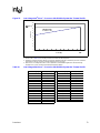
The filter requirements are illustrated in Figure 1.
NOTES:
1. Diagram not to scale.
2. No specifications for frequencies beyond f
core
(core frequency).
3. f
peak
, if existent, should be less than 0.05 MHz.
4. f
core
represents the maximum core frequency supported by the platform.
Table 3. BSEL[1:0] Frequency Table
BSEL1 BSEL0 Bus Clock Frequency
00Reserved
01Reserved
10200MHz
11Reserved
Figure 1. Phase Lock Loop (PLL) Filter Requirements
CS00141
0.2 dB
0 dB
x dB
–28 dB
–34 dB
66 MHz 1.67 GHz1 MHz1 HzDC fpeak fcore
Passband
High
Frequency
<50 kHz 500 MHz

16 Datasheet
2.4 Voltage Identification (VID)
The Voltage Identification (VID) specification for the Low Voltage Intel
®
Xeon™ processor with
800 MHz system bus is defined by the Voltage Regulator Module (VRM) and Enterprise Voltage
Regulator-Down (EVRD) 10.0 Design Guidelines. The voltage set by the VID signals is the
maximum voltage allowed by the processor (please see Section 2.11.1 for V
CC
overshoot
specifications). VID signals are open drain outputs, which must be pulled up to V
TT
. Please refer to
Table 12 for the DC specifications for these signals. A minimum voltage is provided in Table 9 and
changes with frequency. This allows processors running at a higher frequency to have a relaxed
minimum voltage specification. The specifications have been set such that one voltage regulator
can operate with all supported frequencies.
Individual processor VID values may be calibrated during manufacturing such that two devices at
the same core speed may have different default VID settings. This is reflected by the VID Range
values provided in Table 9. Refer to the Intel
®
Xeon™ Processor with 800 MHz System Bus
Specification Update for further details on specific valid core frequency and VID values of the
processor.
The Low Voltage Intel
®
Xeon™ processor with 800 MHz system bus uses six voltage
identification signals, VID[5:0], to support automatic selection of power supply voltages. Table 4
specifies the voltage level corresponding to the state of VID[5:0]. A ‘1’ in this table refers to a high
voltage level and a ‘0’ refers to a low voltage level. If the processor socket is empty (VID[5:0] =
x11111), or the voltage regulation circuit cannot supply the voltage that is requested, it must disable
itself. See the Voltage Regulator Module (VRM) Voltage Regulator-Down (EVRD) 10.0 Design
Guidelines or Voltage Regulator Module (VRM) for further details.
The Low Voltage Intel
®
Xeon™ processor with 800 MHz system bus provides the ability to
operate while transitioning to an adjacent VID and its associated processor core voltage (V
CC
).
This will represent a DC shift in the load line. It should be noted that a low-to-high or high-to-low
voltage state change may result in as many VID transitions as necessary to reach the target core
voltage. Transitions above the specified VID are not permitted. Table 9 includes VID step sizes and
DC shift ranges. Minimum and maximum voltages must be maintained as shown in Table 10 and
Figure 3.
The VRM or VRD used must be capable of regulating its output to the value defined by the new
VID. DC specifications for dynamic VID transitions are included in Table 9 and Table 10. Please
refer to the Voltage Regulator Module (VRM) and Enterprise Voltage Regulator-Down (EVRD)
10.0 Design Guidelines for further details.
Power source characteristics must be guaranteed to be stable whenever the supply to the voltage
regulator is stable.

Datasheet 17
Table 4. Voltage Identification Definition
VID5 VID4 VID3 VID2 VID1 VID0 V
CC_MAX
VID5 VID4 VID3 VID2 VID1 VID0 V
CC_MAX
0010100.8375 0110101.2125
1010010.8500 1110011.2250
0010010.8625 0110011.2375
1010000.8750 1110001.2500
0010000.8875 0110001.2625
1001110.9000 1101111.2750
0001110.9125 0101111.2875
1001100.9250 1101101.3000
0001100.9375 0101101.3125
1001010.9500 1101011.3250
0001010.9625 0101011.3375
1001000.9750 1101001.3500
0001000.9875 0101001.3625
1000111.0000 1100111.3750
0000111.0125 0100111.3875
1000101.0250 1100101.4000
0000101.0375 0100101.4125
1000011.0500 1100011.4250
0000011.0625 0100011.4375
1000001.0750 1100001.4500
0000001.0875 0100001.4625
111111OFF
1
1011111.4750
011111OFF
1
0011111.4875
1111101.1000 1011101.5000
0111101.1125 0011101.5125
1111011.1250 1011011.5250
0111011.1375 0011011.5375
1111001.1500 1011001.5500
0111001.1625 0011001.5625
1110111.1750 1010111.5750
0110111.1875 0010111.5875
1110101.2000 1010101.6000
NOTES:
1. When this VID pattern is observed, the voltage regulator output should be disabled.

18 Datasheet
2.5 Reserved or Unused Pins
All Reserved pins must remain unconnected. Connection of these pins to V
CC
, V
TT
, V
SS
, or to any
other signal (including each other) can result in component malfunction or incompatibility with
future processors. See Section 5.0 for a pin listing of the processor and the location of all Reserved
pins.
For reliable operation, always connect unused inputs or bidirectional signals to an appropriate
signal level. In a system level design, on-die termination has been included by the processor to
allow end agents to be terminated within the processor silicon for most signals. In this context, end
agent refers to the bus agent that resides on either end of the daisy-chained front side bus interface
while a middle agent is any bus agent in between the two end agents. For end agents, most unused
AGTL+ inputs should be left as no connects as AGTL+ termination is provided on the processor
silicon. However, see Table 6 for details on AGTL+ signals that do not include on-die termination.
For middle agents, the on-die termination must be disabled, so the platform must ensure that
unused AGTL+ input signals which do not connect to end agents are connected to V
TT
via a pull-
up resistor. Unused active high inputs, should be connected through a resistor to ground (V
SS
).
Unused outputs can be left unconnected, however this may interfere with some TAP functions,
complicate debug probing, and prevent boundary scan testing. A resistor must be used when tying
bidirectional signals to power or ground. When tying any signal to power or ground, a resistor will
also allow for system testability. Resistor values should be within ± 20% of the impedance of the
baseboard trace for front side bus signals. For unused AGTL+ input or I/O signals, use pull-up
resistors of the same value as the on-die termination resistors (R
TT
).
TAP, Asynchronous GTL+ inputs, and Asynchronous GTL+ outputs do not include on-die
termination. Inputs and utilized outputs must be terminated on the baseboard. Unused outputs may
be terminated on the baseboard or left unconnected. Note that leaving unused outputs unterminated
may interfere with some TAP functions, complicate debug probing, and prevent boundary scan
testing. Signal termination for these signal types is discussed in the ITP700 Debug Port Design
Guide (See Section 1.2).
All TESTHI[6:0] pins should be individually connected to V
TT
via a pull-up resistor which
matches the nominal trace impedance. TESTHI[3:0] and TESTHI[6:5] may be tied together and
pulled up to V
TT
with a single resistor if desired. However, usage of boundary scan test will not be
functional if these pins are connected together. TESTHI4 must always be pulled up independently
from the other TESTHI pins. For optimum noise margin, all pull-up resistor values used for
TESTHI[6:0] pins should have a resistance value within ± 20% of the impedance of the board
transmission line traces. For example, if the nominal trace impedance is 50 Ω, then a value between
40 Ω and 60 Ω should be used.
N/C (no connect) pins of the processor are not used by the processor. There is no connection from
the pin to the die. These pins may perform functions in future processors intended for platforms
using the Low Voltage Intel
®
Xeon™ processor with 800 MHz system bus.

Datasheet 19
2.6 Front Side Bus Signal Groups
The front side bus signals have been combined into groups by buffer type. AGTL+ input signals
have differential input buffers, which use GTLREF as a reference level. In this document, the term
“AGTL+ Input” refers to the AGTL+ input group as well as the AGTL+ I/O group when receiving.
Similarly, “AGTL+ Output” refers to the AGTL+ output group as well as the AGTL+ I/O group
when driving. AGTL+ asynchronous outputs can become active anytime and include an active
pMOS pull-up transistor to assist during the first clock of a low-to-high voltage transition.
With the implementation of a source synchronous data bus comes the need to specify two sets of
timing parameters. One set is for common clock signals whose timings are specified with respect to
rising edge of BCLK0 (ADS#, HIT#, HITM#, etc.) and the second set is for the source
synchronous signals which are relative to their respective strobe lines (data and address) as well as
rising edge of BCLK0. Asynchronous signals are still present (A20M#, IGNNE#, etc.) and can
become active at any time during the clock cycle. Table 5 identifies which signals are common
clock, source synchronous and asynchronous.

20 Datasheet
NOTES:
1. Refer to Section 4.0 for signal descriptions.
2. The Low Voltage Intel
®
Xeon™ processor with 800 MHz system bus only uses BR0# and BR1#. BR2# and
BR3# must be terminated to V
TT
. For additional details regarding the BR[3:0]# signals, see Section 4.0 and
Section 7.1.
3. The value of these pins during the active-to-inactive edge of RESET# defines the processor configuration
options. See Section 7.1 for details.
4. These signals may be driven simultaneously by multiple agents (wired-OR).
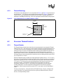
Table 5. Front Side Bus Signal Groups
Signal Group Type Signals
1
AGTL+ Common Clock
Input
Synchronous to BCLK[1:0] BPRI#, BR[3:1]#
2,3
, DEFER#, RESET#, RS[2:0]#,
RSP#, TRDY#
AGTL+ Common Clock I/O Synchronous to BCLK[1:0] ADS#, AP[1:0]#, BINIT#
4
, BNR#
4
, BPM[5:0]#,
BR0#
2,3
, DBSY#, DP[3:0]#, DRDY#, HIT#
4
,
HITM#
4
, LOCK#, MCERR#
4
AGTL+ Source
Synchronous I/O
Synchronous to assoc.
strobe
AGTL+ Strobe I/O Synchronous to BCLK[1:0] ADSTB[1:0]#, DSTBP[3:0]#, DSTBN[3:0]#
AGTL Asynchronous Output Asynchronous FERR#/PBE#, IERR#, PROCHOT#
GTL+ Asynchronous Input Asynchronous A20M#, FORCEPR#, IGNNE#, INIT#
3
, LINT0/
INTR, LINT1/NMI, SMI#
3
, SLP#, STPCLK#
GTL+ Asynchronous Output Asynchronous THERMTRIP#
Front Side Bus Clock Clock BCLK1, BCLK0
TAP Input Synchronous to TCK TCK, TDI, TMS, TRST#
TAP Output Synchronous to TCK TDO
Power/Other Power/Other BOOT_SELECT, BSEL[1:0], COMP[1:0],
GTLREF[3:0], ODTEN, OPTIMIZED/COMPAT#,
PWRGOOD, Reserved, SKTOCC#,
SLEW_CTRL, SMB_PRT, TEST_BUS,
TESTHI[6:0], THERMDA, THERMDC, V
CC
, V
CCA
,
V
CCIOPLL,
V
CCPLL
, VCCSENSE, VID[5:0], V
SS
,
V
SSA
, VSSSENSE, V
TT
, VIDPWRGD, VTTEN
Signals Associated Strobe
REQ[4:0]#,A[16:3]#
3
ADSTB0#
A[35:17]#
3
ADSTB1#
D[15:0]#, DBI0# DSTBP0#, DSTBN0#
D[31:16]#, DBI1# DSTBP1#, DSTBN1#
D[47:32]#, DBI2# DSTBP2#, DSTBN2#
D[63:48]#, DBI3# DSTBP3#, DSTBN3#
Page is loading ...
Page is loading ...
Page is loading ...
Page is loading ...
Page is loading ...
Page is loading ...
Page is loading ...
Page is loading ...
Page is loading ...
Page is loading ...
Page is loading ...
Page is loading ...
Page is loading ...
Page is loading ...
Page is loading ...
Page is loading ...
Page is loading ...
Page is loading ...
Page is loading ...
Page is loading ...
Page is loading ...
Page is loading ...
Page is loading ...
Page is loading ...
Page is loading ...
Page is loading ...
Page is loading ...
Page is loading ...
Page is loading ...
Page is loading ...
Page is loading ...
Page is loading ...
Page is loading ...
Page is loading ...
Page is loading ...
Page is loading ...
Page is loading ...
Page is loading ...
Page is loading ...
Page is loading ...
Page is loading ...
Page is loading ...
Page is loading ...
Page is loading ...
Page is loading ...
Page is loading ...
Page is loading ...
Page is loading ...
Page is loading ...
Page is loading ...
Page is loading ...
Page is loading ...
Page is loading ...
Page is loading ...
Page is loading ...
Page is loading ...
Page is loading ...
Page is loading ...
Page is loading ...
Page is loading ...
Page is loading ...
Page is loading ...
Page is loading ...
Page is loading ...
Page is loading ...
Page is loading ...
-
 1
1
-
 2
2
-
 3
3
-
 4
4
-
 5
5
-
 6
6
-
 7
7
-
 8
8
-
 9
9
-
 10
10
-
 11
11
-
 12
12
-
 13
13
-
 14
14
-
 15
15
-
 16
16
-
 17
17
-
 18
18
-
 19
19
-
 20
20
-
 21
21
-
 22
22
-
 23
23
-
 24
24
-
 25
25
-
 26
26
-
 27
27
-
 28
28
-
 29
29
-
 30
30
-
 31
31
-
 32
32
-
 33
33
-
 34
34
-
 35
35
-
 36
36
-
 37
37
-
 38
38
-
 39
39
-
 40
40
-
 41
41
-
 42
42
-
 43
43
-
 44
44
-
 45
45
-
 46
46
-
 47
47
-
 48
48
-
 49
49
-
 50
50
-
 51
51
-
 52
52
-
 53
53
-
 54
54
-
 55
55
-
 56
56
-
 57
57
-
 58
58
-
 59
59
-
 60
60
-
 61
61
-
 62
62
-
 63
63
-
 64
64
-
 65
65
-
 66
66
-
 67
67
-
 68
68
-
 69
69
-
 70
70
-
 71
71
-
 72
72
-
 73
73
-
 74
74
-
 75
75
-
 76
76
-
 77
77
-
 78
78
-
 79
79
-
 80
80
-
 81
81
-
 82
82
-
 83
83
-
 84
84
-
 85
85
-
 86
86


Fujifilm P4X-0028-2M-800 Datasheet
- Category
- Processors
- Type
- Datasheet
- This manual is also suitable for
Ask a question and I''ll find the answer in the document
Finding information in a document is now easier with AI
Related papers
Other documents
-
Fujitsu S26361-F3099-E828 Datasheet
-
Fujitsu 60Y0311 Datasheet
-
Lenovo AD80583QH0468M Datasheet
-
Supermicro P4X4-028-512K Datasheet
-
Toshiba P4X-0028-512K-533 User manual
-
HP BX80563L5335P Datasheet
-
Intel LE80557RE009512 Datasheet
-
Fujitsu 46M1068 Datasheet
-
HP 46M1069 Datasheet
-
Intel RK80531PC029G0K User manual