UM10301
User Manual for NXP Real Time Clocks PCF85x3, PCF85x63,
PCA8565, PCF2123, and PCA21125
Rev. 2.1 — 23 July 2015
User manual
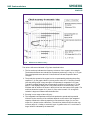
Document information
Info
Content
Keywords
PCF8563, PCF8583, PCF8593, PCA8565, PCF85263, PCF85363,
PCF85063, PCF2123, PCA21125, PCF2120, RTC, real time clock,
timekeeping, crystal, 32.768 kHz, backup.
Abstract
This user manual aims to assist a user of above mentioned Real Time
Clocks in achieving successful design-in and application. It contains
useful hints with respect to electrical schematic and PCB layout as well
as code examples for the well-established NXP PCF8563 and related
Real Time Clocks. Also the more recent Real Time Clocks PCF2123 and
PCA21125 have been taken into account.

NXP Semiconductors
UM10301
User Manual for PCF85x3, PCF85x63, PCA8565, PCF2123, and
PCA21125
UM10301
All information provided in this document is subject to legal disclaimers.
© NXP Semiconductors N.V. 2015. All rights reserved.
User manual
Rev. 2.1 — 23 July 2015
2 of 54
Contact information
For more information, please visit:
http://www.nxp.com
Revision history
Rev
Date
Description
2.1
20150723
Fixed readability issue with certain browsers for Fig 9
2
20150717
Second version. Updated section 6.2
01
20081223
Initial version.
This application note / user manual is a complete update of a previous publication titled:
“Application note for the Philips Real Time Clocks PCF8563,73,83,93” which did not have
an official AN/UM number and is superseded by this document.
The contents were revised with lots of additional information added and errors in the
examples corrected. Additionally it includes information with respect to recently introduced
RTCs.

NXP Semiconductors
UM10301
User Manual for PCF85x3, PCF85x63, PCA8565, PCF2123, and
PCA21125
UM10301
All information provided in this document is subject to legal disclaimers.
© NXP Semiconductors N.V. 2015. All rights reserved.
User manual
Rev. 2.1 — 23 July 2015
3 of 54
1. Introduction
The real time clocks from NXP (previously Philips Semiconductors) have a long tradition
and are used in numerous application fields. Starting from applications like VCR, they
have been used in a wide variety of products like burglar alarm systems, water
sprinklers, (platform) timers, e-metering, time-and-attendance monitoring, building
access control, Point-of-Sale terminals, industrial applications, cars and trucks, telecom
applications such as mobile phones and in gaming machines. In those applications they
are used for functions like keeping calendar time, tariff switching, watch-dog, time
stamping or waking up a system periodically to initiate certain actions, for example
making measurements.
This application note deals with the PCF85x3 family with focus on the PCF8563, and with
the more recent additions to the NXP RTC portfolio PCF2123 and PCA21125. The
PCF2123 is an extremely low power RTC which allows fine tuning of the clock using an
offset register (electronic tuning). PCA21125 is targeted at automotive applications.
Where appropriate, comparisons to other devices are made.
PCF2120 is a low power 32.768 kHz oscillator with two integrated oscillator capacitances
and a CLKOUT pin (32.768 kHz only), but without time, date and configuration registers.
This application note is valid for the PCF2120 as well, particularly information with
respect to oscillator, crystal, crystal and capacitor selection and layout guidelines.
Chapters 2 and 3 describe the features of these RTCs and include a comparison of the
various types. Starting from chapter 4 more technical details are described that need to
be understood in order to achieve successful application of these real time clocks.
Chapters 4 and 5 deal with the power-on reset and voltage-low detection. Chapters 6
through 10 deal with the heart of the RTC; the oscillator, the crystal, crystal and capacitor
selection, accuracy and oscillator tuning. Chapter 11 contains a description of how
century change, leap years and daylight savings time is handled or needs to be handled
in an application. This is followed by some examples in chapter 12 about how to initialize
the RTC and how to set alarm and timer. Providing backup power when the rest of the
system is not powered is covered in chapter 13. In order to make a reliable and accurate
application it is important that the PCB layout is designed carefully and guidelines to
achieve this are listed in chapter 14. This is followed by some further design tips in
chapters 15 and 16 about partial circuit switch down and low power consumption.
Sometimes a component behaves different from what one may initially expect. This does
not imply that it behaves wrongly, but in order to properly deal with it, it is important to be
aware of such behavior. Chapter 17 describes how inaccurate timer performance can be
avoided. Chapter 18 explains why the RTC will lose time if I
2
C and SPI read and write
operations are not finalized within one second of initiating it.
The application note is concluded with a short chapter on trouble shooting.

NXP Semiconductors
UM10301
User Manual for PCF85x3, PCF85x63, PCA8565, PCF2123, and
PCA21125
UM10301
All information provided in this document is subject to legal disclaimers.
© NXP Semiconductors N.V. 2015. All rights reserved.
User manual
Rev. 2.1 — 23 July 2015
4 of 54
2. Features
The NXP real-time clock portfolio includes types for low power, types for automotive and
other high temperature applications and applications that need additional RAM. A third
family of highly accurate temperature compensated real time clocks will be dealt with in a
separate application note. Designed for a range of demanding applications, these real-
time clocks/calendars are driven by a low-power 32.768 kHz quartz oscillator, use the
SPI or I
2
C-bus for serial data transfer, and typically consume less than 1 μW of power.
Key features
• Oscillator requires 32.768 kHz external quartz crystal
• Resolution: seconds, minutes, hours, weekday, day, month, and year in 12- or 24-
hour (military) format. All time and alarm registers are in BCD format. Two types
include a 1/10
th
and 1/100
th
second resolution register
• Clock operating voltage: 1.0 V to 5.5 V or wider, see Table 2
• Low backup current: Ranging from 100 nA to 2 μA at V
DD
= 1 V and T
amb
= 25 °C
• Three line SPI with separate I/O or I
2
C serial interface
• Freely programmable timer and alarm functions, each with interrupt capability
• Freely programmable Watchdog timer
• Programmable clock output for peripheral devices: 32.768 kHz, 1024 Hz, 32 Hz and
1 Hz (not all types)
• One or two integrated oscillator capacitors (connected to the output of amplifier
OSCO in case of only one integrated capacitor)
• Internal power-on reset
• Open-drain interrupt pin
• Wide variety of packages available including naked die
Addresses and data are transferred serially via an SPI bus with a maximum speed of 7.0
Mbps (PCF2123, PCA21125) or via a two-line, bidirectional I
2
C-bus that operates at a
maximum speed of 400 kbps (Fast-Mode, PCF8563 and PCA8565) or 100 kbps
(Standard-Mode, PCF8583 and PCF8593). The built-in word address register is
incremented automatically after each data byte is written or read.
With the PCF8583, the address pin A0 is used to program the software address, so that
two devices can be connected to the same I
2
C-bus without additional hardware.
Each RTC has an internal power-on reset and a programmable clock output with open
drain configuration to drive peripheral devices. A low voltage detector (not included on
the PCF8583,93 and PCA21125) warns if the integrity of all clock functions is no longer
guaranteed.
Power consumption is kept to a minimum in all the devices. The PCF2123 and PCF8563,
optimized for battery-powered applications, consume as little as 100 nA at 2 V and
250 nA at 1 V respectively. With careful selection of the crystal used, the PCF2123
consumes less than 100 nA on a 1.5 V supply.
The seconds, minutes, hours, days, weekdays, months, years as well as the minute
alarm, hour alarm, day alarm and weekday alarm registers are all coded in Binary Coded
Decimal (BCD) format. This format is popular with RTCs for the reason that time and
date in BCD format can easily be displayed in human-readable style without conversion.

NXP Semiconductors
UM10301
User Manual for PCF85x3, PCF85x63, PCA8565, PCF2123, and
PCA21125
UM10301
All information provided in this document is subject to legal disclaimers.
© NXP Semiconductors N.V. 2015. All rights reserved.
User manual
Rev. 2.1 — 23 July 2015
5 of 54
In BCD every digit of the decimal system is represented by a 4-bit group. For example:
157
10
= 0001 0101 0111
BCD
This is not the same as binary representation. It is clear that BCD is not the most efficient
way of coding since every 4-bit group (nibble) could represent numbers 0 through 15, but
in BCD never represents numbers bigger than 9. But for some applications it is
convenient to use BCD and real time clocks are one such application.
Each 8-bit register contains two digits each represented by one nibble. Each 4-bit nibble
can represent the value of 0 up to 9 in BCD, but for some digits the maximum value to be
represented will be lower. The minute register for example will never have to count
higher than 59. The upper most digit can here be represented by 3 bits, freeing up one
bit that can be used to indicate something else.
Not all NXP real-time clocks have exactly the same register implementation and thus the
datasheet of the particular device should be consulted. As an example the register
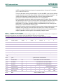
organization of the PCF8563 is given below. Note that this is just one example and that
register organization of other types is not necessarily exactly the same.
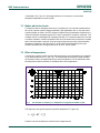
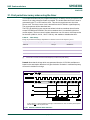
Table 1. Register overview PCF8563
Bit positions labelled as x are not implemented. When setting a register, also a value must be written for the ‘x’ bit positions.
When these are read back, the read back values may differ from what was previously written.
Bit positions labelled with 0 should always be written with logic 0; if read they could be either logic 0 or logic 1.
Address
Register name
Bit 7
Bit 6
Bit 5
Bit 4
Bit 3
Bit 2
Bit 1
Bit 0
00
HEX
control / status 1
TEST1
0
STOP
0
TESTC
0
0
0
01
HEX
control / status 2
0
0
0
TI/TP
AF
TF
AIE
TIE
02
HEX
seconds
VL
<seconds 00 to 59 coded in BCD>
03
HEX
minutes
x
<minutes 00 to 59 coded in BCD>
04
HEX
hours
x
x
<hours 00 to 23 coded in BCD>
05
HEX
days
x
x
<days 01 to 31 coded in BCD>
06
HEX
weekdays
x
x
x
x
x
<weekdays 0 to 6>
07
HEX
months / century
C
x
x
<months 01 to 12 coded in BCD>
08
HEX
years
<years 00 to 99 coded in BCD>
09
HEX
minute alarm
AE
<minute alarm 00 to 59 coded in BCD>
0A
HEX
hour alarm
AE
x
<hour alarm 00 to 23 coded in BCD>
0B
HEX
day alarm
AE
x
<day alarm 01 to 31 coded in BCD>
0C
HEX
weekday alarm
AE
x
x
x
x
<weekday alarm 0 to 6>
0D
HEX
CLKOUT control
FE
x
x
x
x
x
FD1
FD0
0E
HEX
timer control
TE
x
x
x
x
x
TD1
TD0
0F
HEX
timer
<timer countdown value>

NXP Semiconductors
UM10301
User Manual for PCF85x3, PCF85x63, PCA8565, PCF2123, and
PCA21125
UM10301
All information provided in this document is subject to legal disclaimers.
© NXP Semiconductors N.V. 2015. All rights reserved.
User manual
Rev. 2.1 — 23 July 2015
6 of 54
The PCA8565 and PCA21125 oscillators operate over a wider temperature range (up to
125 ºC) and are suitable for use in the harsh environments found within automobiles.
Power consumption remains low — only 700 nA at 2 V. Serial interface is I
2
C or SPI.
All the RTCs have ESD protection that exceeds 2000 V HBM per JESD22-A114, 200 V
MM per JESD22-A115. Charge Device Model values vary from 500 V to 2000 V CDM
per JESD22-C101. Refer to the datasheet of the respective device. Latch-up testing,
performed in accordance with JEDEC Standard JESD78, exceeds 100 mA.
3. Comparison
Table 2 on the next page gives a quick overview of the features, specifications and
differences between the RTCs dealt with in this User Manual. The PCF8573 which
belongs to the PCF85x3 family is no longer in production and has thus not been included
in the table. However, this user manual is useful for this type as well.
Further there are some derived types from the main types listed in the table with small
differences in for example delivery form or the number of integrated oscillator capacitors.
Consult NXP for more details.
3.1 Event counter mode
Two real time clocks, PCF8583 and PCF8593, have an extraordinary feature. It is the
event counter mode which can be selected by setting the appropriate bits in the control
register. In this mode the oscillator is disabled and the oscillator input is switched to a
high impedance state. This mode can be used to count pulses applied to the oscillator
input OSCI. There is no crystal in the circuit and OSCO is left open circuit. The event
counter stores up to 6 digits of data. Events are stored in BCD format. The 6 digits use
three 8 bit registers (hundredth of a second, seconds, and minutes). D5 is the most
significant and D0 the least significant digit. Every digit can contain values ranging from 0
to 9 and thus up to 999 999 events can be stored.
It is also possible to set an event counter alarm. When this function is enabled, the alarm
occurs when the event counter registers match the programmed value. In this event the
alarm flag is set. The inverted value of this flag can be transferred to the interrupt pin by
setting the alarm interrupt enable in the alarm control register. In this mode the timer
increments once for every one, one hundred, ten thousand or 1 million events,
depending on the programmed value of the alarm control register. In all other events, the
timer functions are as in clock mode.
Note that immediately following power-on, all internal registers are undefined and must
be defined by software. It is also possible that upon power-on the device is initially in
event-counter mode in which event the oscillator will not operate until the correct settings
are written into the control registers.
The count value will increment on the falling edge. However, after a new count value has
been programmed at least one rising edge must have occurred before events will be
detected on the falling edge.

NXP Semiconductors
UM10301
User Manual for PCF85x3, PCF85x63, PCA8565, PCF2123, and
PCA21125
UM10301
All information provided in this document is subject to legal disclaimers.
© NXP Semiconductors N.V. 2015. All rights reserved.
User manual
Rev. 2.1 — 23 July 2015
7 of 54
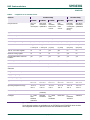
Table 2. Comparison of six real time clocks
Features
PCx85x3 family
PCx212x family
PCF8563
PCA8565
PCF8583
PCF8593
PCF2123
PCA21125
Unique features
Very low
power
consumption
AEC-Q100
automotive
qualification
High
resolution,
RAM, event
counter
High
resolution,
event
counter
Extremely
low power
consumption,
electronic
tuning
AEC-Q100
automotive
qualification
Type of interface
I
2
C
I
2
C
I
2
C
I
2
C
SPI
SPI
Interface bus speed
400 kHz
400 kHz
100 kHz
100 kHz
7 MHz
7 MHz
Scratch pad RAM
no
no
240 bytes
no
no
no
Year / leap year tracking
yes / yes
yes / yes
yes / yes
yes / yes
yes / yes
yes / yes
Year counter
2 digit +
1 century bit
2 digit +
1 century bit
2 bit
(4 years)
2 bit
(4 years)
2 digit
(99 years)
2 digit
(99 years)
100 ms, 10 ms time register
no
no
yes
yes
no
no
Electronic tuning register
no
no
no
no
yes
no
Programmable alarm and timer
functions
yes
yes
yes
yes
yes
yes
Low voltage detector
yes
yes
no
no
yes
no
Event counter mode
no
no
yes
yes
no
no
Option to select between two I
2
C
addresses
no
no
yes
no
no
no
Integrated oscillator capacitor
1 at OSCO
1 at OSCO
1 at OSCO
1 at OSCO
2
1 at OSCO
Supply voltage range
1.8 V – 5.5 V
1.8 V – 5.5 V
2.5 V – 6.0 V
2.5 V – 6.0 V
1.6 V – 5.5 V
1.6 V – 5.5 V
Clock operating voltage
1.0 V – 5.5 V
1.8 V – 5.5 V
1.0 V – 6.0 V
1.0 V – 6.0 V
1.1 V – 5.5 V
1.3 V – 5.5 V
Typical current consumption
250 nA at
V
DD
= 1 V
650 nA at
V
DD
= 3 V
2 μA at
V
DD
= 1 V
1 μA at
V
DD
= 2 V
100 nA at
V
DD
= 2 V
550 nA at
V
DD
= 3 V
Operating temperature range
-40 °C to
+85 °C
-40 °C to
+125 °C
-40 °C to
+85 °C
-40 °C to
+85 °C
-40 °C to
+85 °C
-40 °C to
+125 °C
AEC-Q100 qualified
no
Yes
(TSSOP8)
no
no
no
yes
Packages
U
[1]
, DIP8,
SO8,
TSSOP8,
HVSON10
TSSOP8,
HVSON10
U
[1]
, DIP8,
SO8,
HVQFN20
DIP8, SO8
U
[1]
,
HVQFN16,
TSSOP14
TSSOP14
[1] Naked die
Some derived versions are available such as PCF8563A and PCA8565A which include
two integrated oscillator capacitors and are also available as naked die.

NXP Semiconductors
UM10301
User Manual for PCF85x3, PCF85x63, PCA8565, PCF2123, and
PCA21125
UM10301
All information provided in this document is subject to legal disclaimers.
© NXP Semiconductors N.V. 2015. All rights reserved.
User manual
Rev. 2.1 — 23 July 2015
8 of 54
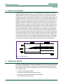
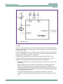
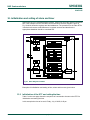
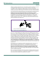
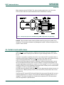
4. Power-on reset (POR)
Traditionally a power-on reset circuit is a circuit that generates a reset pulse once the
supply voltage has reached a certain value upon power-up. The purpose is to ensure a
defined behavior at start-up. This type of power-on reset is not present in these RTCs.
The power-on reset circuit (POR) for these RTCs does not look at the supply voltage, but
instead it is based on an internal reset circuit which is active whenever the oscillator is
stopped, refer to Fig 1. When power is applied to the device it will take some time for the
oscillator to start and during this time the circuit will generate a reset. Also when during
operation the OSCI- or OSCO-pin is pulled to ground, causing oscillation to stop, the
POR will generate a reset pulse. In the reset state the serial bus logic is initialized and all
registers are reset according to the register reset values. Not all registers will be reset.
The only registers that are reset are the ones that control a function i.e. decide on clock
mode, enable an alarm etc. Refer to the datasheet of the respective device for details.
The power on reset duration is thus directly related to the crystal oscillator start-up time.
Due to the long start-up times experienced by these types of circuits on-board testing of
the device would take longer too. In order to speed up this, a mechanism has been built
in to disable the POR (not for PCF8583, PCF8593 and PCF2123). This is called Power-
on reset override. Again, refer to the respective datasheet for details. Once the override
mode has been entered, the device stops immediately being reset and set-up operation
e.g. entry into the external clock test mode, may commence via the serial interface.
Fig 1. Power-on reset
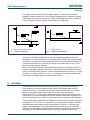
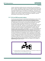
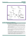
5. Voltage-low detector
PCF8563, PCA8565 and PCF2123 have an on-chip voltage-low detector, see Fig 2 and
Fig 3. When V
DD
drops below a certain limit defined as V
low
, bit VL in the seconds register
of PCF8563 and PCA8565 is set. Generally the VL-bit is intended to indicate that the
time might be wrong, not that it necessarily is wrong. It will be set if one of the following
four conditions occur:
• The power has just been applied;
• The power has dipped down and then recovered;
• The power has gone away and then come back again;
• When the oscillator stops running.

NXP Semiconductors
UM10301
User Manual for PCF85x3, PCF85x63, PCA8565, PCF2123, and
PCA21125
UM10301
All information provided in this document is subject to legal disclaimers.
© NXP Semiconductors N.V. 2015. All rights reserved.
User manual
Rev. 2.1 — 23 July 2015
9 of 54
The implementation in the PCF2123 is slightly different. There a bit OS (Oscillator
Stopped) is present instead of VL. The OS flag is set whenever the oscillator is stopped,
and therefore also when this is due to the supply voltage dropping too low. The flag can
only be cleared by software and only if the oscillator is running again.
(1) Valid for PCF8563 and PCA8565
(2) Valid for PCF2123
Fig 2. Voltage-low detection
Fig 3. Oscillator-stop detection
In the case of PCF8563/PCA8565 bit VL set indicates that the integrity of the clock
information is no longer guaranteed. If the oscillator hasn’t stopped, the clock information
will still be ok, but with V
DD
having dropped below V
low
there is no guarantee that this still
is the case because there is no way to be sure that the oscillator kept running. The VL
flag can only be cleared by software.
Both VL and OS are intended to detect the situation when V
DD
is decreasing slowly, for
example under battery operation. Should V
DD
reach the limit where the flag is set before
power is re-asserted, then the flag VL or OS will indicate that time may be (VL) or is (OS)
corrupted. V
DD
dropping below V
low
or V
osc(min)
in itself does not cause any register to be
reset. Once the oscillator stops some registers will be reset.
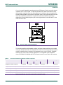
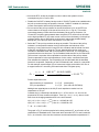
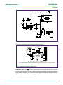
6. Oscillator
A crystal oscillator as used in a real-time clock, see Fig 4, is built on the principle of
Pierce and uses an inverting amplifier with a crystal in the feedback path and load
capacitors C
IN
and C
OUT
to provide the necessary additional phase shift. Some phase
shift is contributed as a result of the amplifier’s non-zero output impedance in
combination with C
OUT
. The oscillator operates at the frequency for which the crystal is
anti-resonant (i.e. parallel resonant) with the total capacitive load of the oscillating circuit
as seen from the pins of the crystal. This total capacitance is called the load capacitance.
The load capacitance is defined as the capacitance seen from the pins of the crystal and
is formed by C
IN
, C
OUT
and C
STRAY
indicated in Fig 4. Electrically the crystal’s C
0
is also a
load capacitance which affects oscillator characteristics. However, it is not part of the
defined ‘load capacitance’. During manufacturing the crystal is tuned to the specified
frequency with a specified load capacitance connected to the crystal. Since C
0
is part of
the crystal, it is automatically taken into account during the adjustment procedure.

NXP Semiconductors
UM10301
User Manual for PCF85x3, PCF85x63, PCA8565, PCF2123, and
PCA21125
UM10301
All information provided in this document is subject to legal disclaimers.
© NXP Semiconductors N.V. 2015. All rights reserved.
User manual
Rev. 2.1 — 23 July 2015
10 of 54
C
STRAY
is a result of parasitic capacitances due to PCB traces, IC pins etc. and is directly
in parallel with C
0
of the crystal. In a practical situation care needs to be taken to keep
these parasitic capacitances as low as possible since it will add to the load capacitance
and this load capacitance must meet the specified value for the crystal that is being used.
If the load capacitance presented to a crystal is smaller than what the crystal was
designed for, the oscillation frequency will be too high and thus if used with an RTC, the
clock will run too fast.
Fig 4. Pierce Oscillator equivalent diagram
The inverting amplifier (with feedback resistor, and drive resistor which are not included
in Fig 4) is incorporated within the integrated circuit device. On the other hand, the quartz
crystal is a discrete device external to the integrated circuit. In the PCF85x3, PCA8565
and PCF2123, PCA21125 the output capacitor C
OUT
is integrated on the integrated
circuit. PCF8563A, PCA8565A and PCF2123 also include C
IN
, see Table 3 for overview.
Table 3. Overview of internal and external oscillator capacitors
Features
PCx85x3 family
PCx212x family
PCF8563
PCA8565
PCF8583
PCF8593
PCF2123
PCA21125
Integrated oscillator capacitor
1 at OSCO
1 at OSCO
1 at OSCO
1 at OSCO
2
1 at OSCO
Targeted crystal load capacitance
12.5 pF
12. 5 pF
12.5 pF
12. 5 pF
7 pF
[1]
12.5 pF
Value of integrated C
IN
, typ.
-
-
14 pF
-
Value of integrated C
OUT
, typ.
25 pF
25 pF
40 pF
25 pF
14 pF
25 pF
Theoretically required at pin OSCI
25 pF
25 pF
18 pF
25 pF
0 pF
25 pF
[1] Can be used with 9 pF and 12.5 pF as well if external capacitance is added

NXP Semiconductors
UM10301
User Manual for PCF85x3, PCF85x63, PCA8565, PCF2123, and
PCA21125
UM10301
All information provided in this document is subject to legal disclaimers.
© NXP Semiconductors N.V. 2015. All rights reserved.
User manual
Rev. 2.1 — 23 July 2015
11 of 54
The values used in practice will be a bit smaller than the theoretically required values due
to parasitic capacitances present in the application which add to the external physical
capacitor.
For the PCF2123 the integrated C
IN
and C
OUT
are dimensioned for a crystal which
requires a load capacitance of 7 pF. If a crystal with required load capacitance of 12.5 pF
is used still a small external capacitor is required, otherwise the clock will run too fast.
For the other types the input capacitor C
IN
is external and needs to be mounted on the
printed circuit board. The power consumed by the oscillator circuit is through the amplifier
and losses in R
1
of the crystal. Oscillation will start if the loop gain at 360° phase shift is
higher than one. The oscillator amplitude increases until the over-all loop gain is reduced
to exactly 1 through either nonlinear effects of the amplifier (self-limiting Pierce) or
through some form of AGC (Automatic Gain Control) designed in into the amplifier.
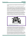
The resonating frequency can be pulled by changing the value of the capacitor at OSCI
or by adding a variable capacitor C
T
at OSCO as shown in Fig 5. External capacitors at
OSCI and OSCO should be connected to GND, except for PCF8573, PCF8583 and
PCF8593. For the latter three it is better to connect these external capacitors to V
DD
instead because these devices are manufactured in a process that has the substrate
connected to V
DD
(n-substrate). In the other RTCs the substrate is at V
SS
(p-substrate).
(1) For PCF8573, PCF8583 and PCF8593 connect C
IN
and C
OUT
(and C
T
if applicable) to V
DD
Fig 5. Oscillator frequency determining components
The reactive components indicated in Fig 4 and Fig 5 determine the oscillating
frequency. Near the resonance frequency the equivalent circuit of the crystal consists of
the motional inductance L
1
, the motional capacitance C
1
and the motional resistance R
1
(in various literature also called series resistance R
S
). In parallel with this series circuit is
the static or shunt capacitance C
0
. It is the sum of the capacitance between the
electrodes and the capacitance added by the leads and mounting structure. If one were
to measure the reactance of the crystal at a frequency far away from a resonance
frequency, it is the reactance of this capacitance that would be measured.
When a crystal is chosen, such a crystal has a specified load capacitance C
L
. During
production the crystal manufacturer has adjusted the resonance frequency of the crystal
using exactly this capacitance as the load for the crystal. The actual value of C
L
as seen
by the crystal in the application is determined by the external circuitry and parasitic
capacitances. The external components of the oscillator have to be chosen such that the

NXP Semiconductors
UM10301
User Manual for PCF85x3, PCF85x63, PCA8565, PCF2123, and
PCA21125
UM10301
All information provided in this document is subject to legal disclaimers.
© NXP Semiconductors N.V. 2015. All rights reserved.
User manual
Rev. 2.1 — 23 July 2015
12 of 54
actual value of C
L
matches the specified value of C
L
. If there is mismatch the crystal will
not run exactly at its specified frequency resulting in the clock running slow or fast.
The crystal manufacturer can manufacture crystals for any load capacitance, but in
practice some standard values are used. For use in real-time clocks you may find
crystals specified for load capacitances of 7 pF, 9 pF and 12.5 pF with 12.5 pF the most
common value.
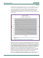
(1) Frequency on the left scale and the equivalent deviation from the nominal frequency in ppm on
the right scale
Fig 6. Graph of oscillator frequency as function of load capacitance C
L
Fig 6 depicts the influence of the load capacitance applied to the crystal on the oscillator
frequency. The lower curve represents a crystal with a specified C
L
of 7 pF, the upper
curve represents a crystal with a specified C
L
of 12 pF. From this graph it is obvious that
the 7 pF crystal is more sensitive to deviations from the specified C
L
. If the applied C
L
is 1
pF lower than specified, the frequency deviation will be 18 ppm, whereas the 12.5 pF
crystal will only show a frequency deviation of 6 ppm if the applied C
L
is 1 pF below the
specified value. This is not surprising since the same absolute change in load
capacitance is a larger relative change if the load capacitance is smaller. A lower load
capacitance however will result in lower power consumption and in cases where this is
an important requirement a crystal with lower required C
L
could be selected.
Now in order to determine the value of C
L
resulting from C
IN
, C
OUT
(plus C
T
if mounted)
and C
STRAY
it is necessary to realize that seen from the crystal, C
IN
and C
OUT
are

NXP Semiconductors
UM10301
User Manual for PCF85x3, PCF85x63, PCA8565, PCF2123, and
PCA21125
UM10301
All information provided in this document is subject to legal disclaimers.
© NXP Semiconductors N.V. 2015. All rights reserved.
User manual
Rev. 2.1 — 23 July 2015
13 of 54
effectively in series; the 32 kHz signal goes from OSCI through C
IN
to ground, via ground
to C
OUT
and then through C
OUT
to OSCO. In parallel with this series circuit is C
STRAY
. For
the remainder of this discussion, whenever in formulas C
OUT
is written this represents
either the value of C
OUT
only, or in case a trimming capacitor C
T
is present too, the sum
of C
OUT
and C
T
. Now the load capacitance C
L
is given by:
STRAY
OUTIN
OUTIN
L
C
CC
CC
C +
+
⋅
=
Since C
0
is in parallel with C
L
the total capacitance in parallel with the motional arm
L
1
-C
1
-R
1
is given by
0
CC
CC
CC
C
STRAY
OUTIN
OUTIN
PAR
++
+
⋅
=
The motional arm is a series circuit, which forms a closed circuit because there is a
capacitance C
PAR
connected in parallel to this series circuit. Of course the crystal itself
can’t oscillate stand alone, but the equivalent capacitance C which determines together
with L
1
the resulting resonance frequency is now given by the series circuit of C
PAR
and
C
1
. Thus C is given by
++
+
⋅
+
++
+
⋅
⋅
=
01
01
CC
CC
CC
C
CC
CC
CC
C
C
STRAY
OUTIN
OUTIN
STRAY
OUTIN
OUTIN
Typical values for crystal parameters are given in Table 4. From these values it is clear
that C
1
is several orders of magnitudes smaller than the other capacitances in this
expression and therefore C
1
dominates. C will be in the order of magnitude of C
1
but it
will be a bit smaller as a result of C
PAR
in series.
With
LC
1
=
ω
and
1
11
RC
Q ⋅=
ω
the resulting resonance frequency and quality
factor can be calculated.
Because C
1
is orders of magnitude smaller than the other capacitances Q can be
approximated by
11
11
RC
Q
a
⋅=
ω
Taking the numbers from Table 4 yields for L
1
and Q:

NXP Semiconductors
UM10301
User Manual for PCF85x3, PCF85x63, PCA8565, PCF2123, and
PCA21125
UM10301
All information provided in this document is subject to legal disclaimers.
© NXP Semiconductors N.V. 2015. All rights reserved.
User manual
Rev. 2.1 — 23 July 2015
14 of 54
( ) ( )
H
Cf
L 11234
101.2327682
1
2
1
15
2
1
2
0
1
=
⋅⋅⋅
=
⋅⋅
=
−
ππ
( )
( )
42053
1055101.2327682
1
2
1
315
110
=
⋅⋅⋅⋅⋅
=
⋅⋅⋅
=
−
π
π
RCf
Q
This L of around 11000 H resulting in a Q of around 42000 explains why starting up the
oscillator as well as stopping it can easily take more than a second. An oscillating quartz
crystal is actually a mechanical oscillation and starting or stopping this takes time.
Calculations of startup time and more in-depth theory about the oscillator and load
capacitance are beyond the scope of this user manual, but can be found in AN10716
“Background information and theory related to Real Time Clocks and crystals”.
The use of AGC’s improve start up by high drive initially to get it going and then reduce
drive for low power.
Table 4. Typical values for crystal and surrounding capacitors
Parameter
Value
Unit
Source
f
0
32768
Hz
[2]
∆f / f
0
±100
ppm
[2]
Aging; ∆f / f
0
±3…±5
ppm
[2]
B, freq(T)
-0.035
ppm / °C
2
[2]
C
1
2.1
fF
[2]
C
0
1.2…1.5
pF
[2]
C
IN
25 ± 10
pF
[1]
C
IN
, temp co.
+47
ppm/°C
[1]
R
1
50…80
kΩ
[2]
C
T
variable
4…25
pF
[3]
C
T
, temp co.
300
ppm/°C
[3]
C
T
fixed 0603
Any
pF
[4]
C
T
fixed, tc
±30 for C0G
ppm/°C
[4]
Sources for values in table 4:
[1] NXP, Datasheet PCF8563, February 2008.
[2] Product Data Sheets, MicroCrystal.
[3] Murata TZB04 trim capacitor
[4] Vishay Beyschlag, datasheet ceramic multilayer capacitor, C0G

NXP Semiconductors
UM10301
User Manual for PCF85x3, PCF85x63, PCA8565, PCF2123, and
PCA21125
UM10301
All information provided in this document is subject to legal disclaimers.
© NXP Semiconductors N.V. 2015. All rights reserved.
User manual
Rev. 2.1 — 23 July 2015
15 of 54
6.1 Oscillation allowance
Fig 4 shows the Pierce oscillator schematic with the external crystal. For an oscillation to
take place the real component of the oscillator impedance has to be larger than the
motional resistance R
1
(sometimes called R
S
or ESR). If R
1
is too large no oscillation will
take place since no operating point can be reached.
Similarly, if the supply voltage is too low or the temperature is too low, no oscillation can
build up.
A method to test how much margin the design has is to include a resistor R
X
in series
with the crystal. The value of the resistor is changed (a trimmer is useful here) to see at
which values of R
X
oscillation starts and stops. Starting from a large value of R
X
the
resistance is lowered until oscillation starts. This value of R
X
is called R
X-start
. Now the
value is increased again until oscillation stops, R
X
is called R
X-stop
.
The oscillation allowance OA is defined as:
OA = R
X-start
+ R
1
As a rule of thumb, the motional resistance of the crystal chosen should be
5
1
OA
R ≤
This test can be done in the lab under room temperature. This should give enough safety
margins to allow for production spread of IC and crystal and to deal with the increasing
value of R
1
under influence of increased temperature.
6.2 Using an external oscillator
It is possible to supply a clock signal from an external oscillator instead of using the
internal oscillator if for some reason it is desired to not use the internal oscillator. In this
case no crystal will be connected to the OSCI and OSCO pins. Instead, the external
oscillator is connected to the OSCI pin while the OSCO pin must be left floating. The
external oscillator should provide a signal with about 500 mV amplitude, swinging around
a +250 mV bias (i.e. never going negative) as would be seen if the crystal was being
used. These are general guidelines and some real time clocks require different input as
discussed below. Additionally, values mentioned here are for guideline only and for every
application correct operation must be verified.
6.2.1 RTC family PCF85x63, PCF8563, PCF8564A, PCA8565, PCF8523
A good starting point is to supply a signal with amplitude between 500 mV and 1000 mV,
with the bias such that the signal doesn’t go negative and operates in the same region as
would have been the case with a crystal.
Suppose that amplitude of the external CLK is 5 V (from 0 V to 5 V). Using 1 M and 100 k
resistors the signal could be reduced to (100 / 1100) x 5 V = 450 mV. This is better in line
with the signals that the internal circuitry handles when an external crystal is used as is
the case in the standard application. This reduced signal can then be applied to the OSCI

NXP Semiconductors
UM10301
User Manual for PCF85x3, PCF85x63, PCA8565, PCF2123, and
PCA21125
UM10301
All information provided in this document is subject to legal disclaimers.
© NXP Semiconductors N.V. 2015. All rights reserved.
User manual
Rev. 2.1 — 23 July 2015
16 of 54
pin directly or via a small capacitor of e.g. 22 pF - 100 pF. Alternatively a capacitive
divider circuit can be used to reduce the signal amplitude.
Either square or sine wave is ok.
6.2.2 PCF2123
As other RTCs, but the required amplitude should be somewhat smaller, around 300 mV.
6.2.3 PCF8583 and PCF8593
When used with a crystal the signal would swing around a bias about 100 mV below
VDD. If these RTCs are fed with an external signal, it should be either AC coupled, or
swinging with amplitude of around 1 V below VDD, where the lower value may be lower
than 1 V below VDD.
7. Crystal and crystal selection
Select a crystal of the tuning fork type with a nominal frequency of 2
15
Hz = 32768 Hz.
The allowed tolerance depends on the requirements for the application and on whether a
trimming capacitor will be used. If a trimming capacitor will be used even a tolerance of
±100 ppm is ok since it can be compensated. Either through hole or surface mount
crystals can be used where the latter provide the smallest dimensions which makes the
circuit less susceptible to noise pick up.
As previously pointed out crystals used for RTCs come in three versions, optimized for
three standard values for C
L
with 12.5 pF the most common. Generally, an RTC using a
12.5 pF crystal has a timekeeping current of about 1.6x more than an RTC using a 7 pF
crystal. If lowest power consumption is a key consideration, a 7 pF crystal (some
manufacturers use 6 pF) should be selected. The PCF2123 has been optimized for use
with such a crystal. The other RTCs include load capacitance optimized for a 12.5 pF
crystal. Using a 7 pF crystal would require an external capacitor of about 9.7 pF and thus
the capacitances at OSCI and OSCO would not be balanced. In general this may have a
detrimental influence on start-up behavior but no problems are expected when a 7 pF
crystal is used in combination with the PCF8563 because it uses an AGC in its oscillator.
An oscillator using a 12.5 pF crystal will be more stable and less susceptible to noise and
parasitic capacitances. One reason for this is that the capacitors on the input and output
will have higher values and therefore create a higher load for noise. Further these higher
values make the parasitic capacitance relatively smaller for the same PCB.
Besides technical considerations there are also procurement issues. Crystals designed
for a 12.5 pF load capacitance are readily available through many distributors. Crystals
designed for a load capacitance of 7 pF or 9 pF are not as readily available and may
have longer lead times or require a minimum quantity to be purchased.
The series resistance R
1
should ideally remain below 50 kΩ. If higher values are used
(up to 100 kΩ is ok) the current consumption of the oscillator will increase a bit. If the
value is really too high startup problems may occur, but up to 100 kΩ no startup
problems are expected. See 6.1”Oscillation allowance”.
The frequency accuracy of the oscillator depends mainly on the accuracy of the crystal
and on how well the crystal is matched to the oscillator capacitive load (C
L
). A too small
capacitive load results in the oscillator running fast, if the capacitive load is greater than
what the crystal was designed for the oscillator and thus clock runs slow. This initial error

NXP Semiconductors
UM10301
User Manual for PCF85x3, PCF85x63, PCA8565, PCF2123, and
PCA21125
UM10301
All information provided in this document is subject to legal disclaimers.
© NXP Semiconductors N.V. 2015. All rights reserved.
User manual
Rev. 2.1 — 23 July 2015
17 of 54
is indicated in Fig 7 as ∆f
off
. The largest influence on accuracy is a result of the
temperature dependence of the crystal.
7.1 Modes which don’t work
To keep time with an adequate accuracy it is necessary to use a quartz crystal and thus
the use of a quartz crystal is always assumed in this application note. A very low power
crystal oscillator as used in an RTC requires a different set of parameters compared to a
universal oscillator accepting crystals, RC- and LC networks or a ceramic resonator. The
oscillator circuit is not designed for operating with RC or LC networks neither for use with
a ceramic resonator. Ceramic resonators have a much shorter start up time than crystals,
about 100 times faster. However, they have lower frequency accuracy (initial tolerance,
temperature variations, drift) and since in an RTC accurate timekeeping is the goal,
ceramic resonators are not a good choice for an RTC. Use a crystal.
7.2 Effect of temperature
A tuning fork crystal is usually cut such that its frequency over temperature is a parabolic
curve centered around 25 °C, see Fig 7. This means that a tuning fork crystal oscillator
will resonate close to its target frequency at room temperature, but will slow down when
the temperature either increases or decreases from room temperature.
Fig 7. The deviation in frequency vs. temperature of a typical 32.768 kHz crystal
The frequency of a typical crystal at a specific temperature T is given by:
( )
[ ]
2
00
1 TTBff −+=
Further f
0
can be considered to consist of two components as

NXP Semiconductors
UM10301
User Manual for PCF85x3, PCF85x63, PCA8565, PCF2123, and
PCA21125
UM10301
All information provided in this document is subject to legal disclaimers.
© NXP Semiconductors N.V. 2015. All rights reserved.
User manual
Rev. 2.1 — 23 July 2015
18 of 54
offnom
fff +=
0
Here f
nom
is the nominal frequency as specified and f
off
the offset from this nominal
frequency which is a result of production spread, both at room temperature.
( )
[ ]
2
0
1 TTBfff
offnom
−+⋅
+=
For the frequency deviation
nom
nom
nom
f
ff
f
f
−
=
∆
and expressed in ppm, this results in:
( )
( )
[ ]
6
2
0
2
0
101 ⋅
−++−=
∆
TTB
f
f
TTB
f
f
nom
off
nom
(7.1)
In these equations f is the frequency, f
0
is the frequency at room temperature, B is the
parabolic coefficient, T is the temperature and T
0
is the turnover temperature where the
apex of the drift versus temperature curve occurs.
Three variables in equation (7.1) influence the frequency as a function of temperature.
These are the parabolic coefficient B, the turnover temperature T
0
and the room
temperature offset f
off
. The crystal manufacturer specifies these parameters and typical
values are B = - 0.035 ppm/°C
2
to - 0.04 ppm/°C
2
, T
0
= 25 °C, ∆T
0
= ± 5 °C and
f
off
= 30 ppm. The coefficient B has a very small spread for various crystals of one type,
but it has the largest effect on the parabolic nature of the frequency deviation as a
function of temperature. Variation in the turnover temperature T
0
will shift the deviation
curve left or right, variation in the offset at room temperature will shift it up or down. In
practice the combination of variation in T
0
and offset at room temperature easily results in
a (lack of) accuracy of ±30 ppm at room temperature which equates to a time deviation of
around 15 minutes per year.
Application note AN10652 “Improved timekeeping accuracy with PCF8563 using external
temperature sensor” describes how accuracy over temperature can be improved using
an external temperature sensor and a software algorithm. It can be used for the other
RTCs in this manual too in conjunction with the respective datasheets.
PCF2123 contains an offset register which allows fine tuning of the clock. This can be
used to compensate for crystal aging and temperature variations. See section 10.1.
Automotive RTCs PCA8565 and PCA21125 operate also at high ambient temperatures
of 125 °C. Obviously also the crystal selected for these applications should be able to
handle this temperature. Generally metal can quartzes are not recommended for high
temperatures because the thermal cycling (expansion of package) will cause leakages in
the hermetically sealed package. Micro Crystal of Switzerland manufactures a wide
range of crystals which include crystals designed to operate up to 125 °C.

NXP Semiconductors
UM10301
User Manual for PCF85x3, PCF85x63, PCA8565, PCF2123, and
PCA21125
UM10301
All information provided in this document is subject to legal disclaimers.
© NXP Semiconductors N.V. 2015. All rights reserved.
User manual
Rev. 2.1 — 23 July 2015
19 of 54
8. Capacitors and capacitor selection
The influence of temperature on the accuracy of the RTC application due to the
temperature coefficient of the capacitances C
IN
and C
OUT
is far less than due to the
temperature coefficient of the crystal. Nevertheless it is good to be aware of some
differences between the various types of capacitors (dielectric) around.
Ceramic capacitors tend to have low inductance because of their flat plate construction.
Most other types of capacitor are wound and thus inductive. Nowadays SMD capacitors
are dominant in small signal applications.
The EIA (Electronic Industries Alliance) has issued EIA-535 which defines capacitor
dielectric classes. Class I and Class II dielectrics have been defined. Within these
classes several types of dielectric exist. The most common ceramic types are C0G/NP0,
X7R, Y5V and Z5U but others exist too.
C0G (EIA) or NP0 is the highest quality of these with the lowest capacitance /
temperature dependence (Negative-Positive Zero), but has a lower permittivity, which
means that its capacitance range is more restricted. NP0 refers to the shape of the
capacitor’s temperature graph and for NP0 this graph is nearly flat. It also exhibits a
negligible capacitance and dissipation factor change with voltage or frequency.
X7R is a reasonably stable high-permittivity dielectric which allows capacitance values up
to 1μF into a reasonable package. The available range is in the order from 100 pF to
22 μF in SMT, larger values are available in leaded packages. X7R formulations fall into
EIA Class II materials. X7R is the most popular of these intermediate dielectric constant
materials. Its capacitance variation as a function of temperature is within ±15 % from
-55 °C to +125 °C. This capacitance change is non-linear and therefore difficult to
express in ppm/°C since it changes over the temperature range. Capacitance for X7R
varies under the influence of electrical operating conditions such as voltage and
frequency. This rules out many applications, leaving only the general purpose
applications like coupling and decoupling. The leakage current is sufficiently low.
Y5V formulations are for general-purpose use in a limited temperature range. Available
range is from 1 nF to 22 μF in SMT, larger in leaded packages. They have a wide
capacitance change of +22 % to –82 % over the operating temperature range of –30°C
to +85°C. As an example, at 31% of the rated voltage (5 V over a 16 V capacitor) the
resulting capacitance will have reduced to a quarter of the rated value. The effective
decoupling capacitance present may thus be much less than expected. Y5V’s high
dielectric constant allows the manufacture of the highest capacitance value in a given
case size. These characteristics make Y5V ideal for decoupling applications within
limited temperature range. When specifying the values, the dependence on temperature
and applied voltage must be taken into account.
Z5U shows in comparison to the previous types a much worse performance. Its
capacitance changes by over 50 % with changes in temperature and applied voltage. Its
temperature range is only +10 °C to +85 °C. Its initial tolerance can be as high as -20 %
to +80 %. Its only redeeming feature is its high permittivity which allows high capacitance
values, typically ranging from 1 nF to 4.7 µF. Good for bypass and coupling applications.
It has low price, small size and low temperature stability.
Conclusion: For the oscillator only C0G types should be used. This will almost always
automatically be the case since the other types are usually not available in such small
values. For the decoupling of the RTC, use a capacitor with X7R dielectric. Using SMD

NXP Semiconductors
UM10301
User Manual for PCF85x3, PCF85x63, PCA8565, PCF2123, and
PCA21125
UM10301
All information provided in this document is subject to legal disclaimers.
© NXP Semiconductors N.V. 2015. All rights reserved.
User manual
Rev. 2.1 — 23 July 2015
20 of 54
packages results in the lowest parasitic inductances and the small dimensions enable the
smallest loops which reduces sensitivity to EMI.
A more expensive alternative for the decoupling X7R capacitor is a film capacitor using
Polyethylene naphthalate (PEN), another form of polyester. It has very good heat
resistance, but is otherwise much like polyester. It is available in larger sizes than C0G
ceramic, lower temperature drift than polyester, and lower leakage than X7R. PEN
capacitors are available to 125 °C. It is commonly found in SMD capacitors, including
large values (>1 μF).
9. Accuracy
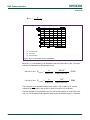
How accurate is accurate??
The international System of Units (SI) has defined the second as the duration of
9,192,631,770 cycles of radiation corresponding to the transition between two energy
levels of the ground state of the cesium-133 atom. This definition makes the cesium
oscillator (often called an atomic clock) the primary standard for time and frequency
measurements. Its accuracy is extremely high with deviations of only a second per
several million years. This equates to accuracy in the order of 10
-8
ppm or better.
In dealing with RTCs it is common to express accuracy in ppm, parts per million. But
what does it mean in more human units? A clock going too fast 1 s/day has an accuracy
of 1 / (number of seconds in a day) = 1 / (24 x 3600) = 11.57 ppm. The other way around,
20 ppm is about 1 minute per month.
1 s/week = 1.65 ppm, 1 s/month = 0.4 ppm and 1 s/year = 0.031 ppm. In contrast, a good
mechanical watch has a deviation of less than 12 s/day or 1300 ppm.
Fig 8 compares the magnitude of the different spreads and variations.
The RTC accuracy dominantly depends on the parameters of the resonating crystal. The
initial frequency tolerance f
off
can be compensated by tuning the external capacitance.
The temperature coefficient of the external capacitances has almost no effect. The main
contribution comes from the temperature coefficient of the crystal. In contrast to AT-cut
crystals tuning fork crystals have the parabolic temperature dependence indicated in
Fig 7 which results in a slowdown of the clock if the temperature is lower or higher than
T
0
which is in the range of 25 to 28 degrees. The same type of crystal is also used in
wrist watches and the turnover temperature of the crystal matches well with the
temperature at the wrist which is typically about 28 °C and quite stable.
Page is loading ...
Page is loading ...
Page is loading ...
Page is loading ...
Page is loading ...
Page is loading ...
Page is loading ...
Page is loading ...
Page is loading ...
Page is loading ...
Page is loading ...
Page is loading ...
Page is loading ...
Page is loading ...
Page is loading ...
Page is loading ...
Page is loading ...
Page is loading ...
Page is loading ...
Page is loading ...
Page is loading ...
Page is loading ...
Page is loading ...
Page is loading ...
Page is loading ...
Page is loading ...
Page is loading ...
Page is loading ...
Page is loading ...
Page is loading ...
Page is loading ...
Page is loading ...
Page is loading ...
Page is loading ...
-
 1
1
-
 2
2
-
 3
3
-
 4
4
-
 5
5
-
 6
6
-
 7
7
-
 8
8
-
 9
9
-
 10
10
-
 11
11
-
 12
12
-
 13
13
-
 14
14
-
 15
15
-
 16
16
-
 17
17
-
 18
18
-
 19
19
-
 20
20
-
 21
21
-
 22
22
-
 23
23
-
 24
24
-
 25
25
-
 26
26
-
 27
27
-
 28
28
-
 29
29
-
 30
30
-
 31
31
-
 32
32
-
 33
33
-
 34
34
-
 35
35
-
 36
36
-
 37
37
-
 38
38
-
 39
39
-
 40
40
-
 41
41
-
 42
42
-
 43
43
-
 44
44
-
 45
45
-
 46
46
-
 47
47
-
 48
48
-
 49
49
-
 50
50
-
 51
51
-
 52
52
-
 53
53
-
 54
54