
MoBL-USB™ FX2LP18 USB Microcontroller
CY7C68053
Cypress Semiconductor Corporation • 198 Champion Court • San Jose, CA 95134-1709 • 408-943-2600
Document # 001-06120 Rev *F Revised September 9th 2006
1.0 CY7C68053 Features
• USB 2.0 – USB-IF High-Speed and Full-Speed Compliant
(TID# 40000188)
• Single-chip integrated USB 2.0 transceiver, smart SIE, and
enhanced 8051 microprocessor
• Ideal for mobile applications (cell phone, smart phones,
PDAs, MP3 players)
— Ultra low power
— Suspend current: 20 µA (typical)
• Software: 8051 code runs from:
— Internal RAM, which is loaded from EEPROM
• 16 kBytes of on-chip Code/Data RAM
• Four programmable BULK/INTERRUPT/ISOCHRONOUS
endpoints
— Buffering options: double, triple, and quad
• Additional programmable (BULK/INTERRUPT) 64-byte
endpoint
• 8- or 16-bit external data interface
• Smart Media Standard ECC generation
• GPIF (General Programmable Interface)
— Allows direct connection to most parallel interface
— Programmable waveform descriptors and configuration
registers to define waveforms
— Supports multiple Ready (RDY) inputs and Control (CTL)
outputs
• Integrated, industry standard enhanced 8051
— 48 MHz, 24 MHz, or 12 MHz CPU operation
— Four clocks per instruction cycle
— Three counter/timers
— Expanded interrupt system
— Two data pointers
• 1.8V core operation
• 1.8V - 3.3V IO operation
• Vectored USB interrupts and GPIF/FIFO interrupts
• Separate data buffers for the Set-up and Data portions of a
CONTROL transfer
• Integrated I
2
C™ controller, runs at 100 or 400 kHz
• Four integrated FIFO’s
— Integrated glue logic and FIFO’s lower system cost
— Automatic conversion to and from 16-bit buses
— Master or slave operation
— Uses external clock or asynchronous strobes
— Easy interface to ASIC and DSP IC’s
• Available in Industrial temperature grade
• Available in one lead-free package with up to 24 GPIO’s
— 56-pin VFBGA (24 GPIO’s)
x20
PLL
/0.5
/1.0
/2.0
8051 Core
12/24/48 MHz,
Four Clocks/Cycle
I
2
C
VCC
1.5K
D+
D–
Address (16) / Data Bus (8)
GPIF
CY
Smart
USB
1.1/2.0
Engine
USB
2.0
XCVR
16 KB
RAM
4 KB
FIFO
Integrated
Full- and High-speed
XCVR
Additional I/Os (24)
CTL (3)
RDY (2)
24 MHz
Ext. XTAL
Enhanced USB Core
Simplifies 8051 Code
“Soft Configuration”
Easy Firmware Changes
FIFO and Endpoint Memory
(master or slave operation)
General
Programmable I/F
Abundant I/O
High-performance micro
using standard tools
with lower-power options
Master
Connected for
Full-Speed
ECC
MoBL-USB FX2LP18
To Baseband processors/
Application processors/
ASICS/DSPs
8/16
Up to 96 MBytes/sec
Burst Rate
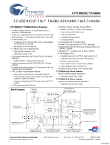
Block Diagram
[+] Feedback

CY7C68053
Document # 001-06120 Rev *F Page 2 of 39
Cypress Semiconductor Corporation’s MoBL-USB FX2LP18
(CY7C68053) is a low-voltage (1.8 volt) version of the EZ-
USB
®
FX2LP (CY7C68013A), which is a highly integrated,
low-power USB 2.0 microcontroller. By integrating the USB 2.0
transceiver, serial interface engine (SIE), enhanced 8051
microcontroller, and a programmable peripheral interface in a
single chip, Cypress has created a very cost-effective solution
that provides superior time-to-market advantages with low
power to enable bus powered applications.
The ingenious architecture of MoBL-USB FX2LP18 results in
data transfer rates of over 53 Mbytes per second, the
maximum allowable USB 2.0 bandwidth, while still using a low-
cost 8051 microcontroller in a package as small as a 56
VFBGA (5 mm x 5 mm). Because it incorporates the USB 2.0
transceiver, the MoBL-USB FX2LP18 is more economical,
providing a smaller footprint solution than USB 2.0 SIE or
external transceiver implementations. With MoBL-USB
FX2LP18, the Cypress Smart SIE handles most of the USB 1.1
and 2.0 protocol in hardware, freeing the embedded microcon-
troller for application-specific functions and decreasing devel-
opment time to ensure USB compatibility.
The General Programmable Interface (GPIF) and
Master/Slave Endpoint FIFO (8- or 16-bit data bus) provide an
easy and glueless interface to popular interfaces such as
ATA,
UTOPIA, EPP, PCMCIA, and most DSP/processors.
The 56VFBGA package is defined for the family.
The MoBL-USB FX2LP18 is also referred to as FX2LP18 in
this document.
2.0 Applications
There are a wide variety of applications for the MoBL-USB
FX2LP18. It is used in cell phone, smart phones, PDAs, and
MP3 players, to name a few.
The ‘Reference Designs’ section of the Cypress web site
provides additional tools for typical USB 2.0 applications. Each
reference design comes complete with firmware source and
object code, schematics, and documentation. For more infor-
mation, visit http://www.cypress.com.
3.0 Functional Overview
The functionality of this chip is described in the sections below.
3.1 USB Signaling Speed
FX2LP18 operates at two of the three rates defined in the USB
Specification Revision 2.0, dated April 27, 2000.
• Full-speed, with a signaling bit rate of 12 Mbps
• High-speed, with a signaling bit rate of 480 Mbps.
FX2LP18 does not support the low-speed signaling mode of
1.5 Mbps.
3.2 8051 Microprocessor
The 8051 microprocessor embedded in the FX2LP18 family
has 256 bytes of register RAM, an expanded interrupt system,
and three timer/counters.
3.2.1 8051 Clock Frequency
FX2LP18 has an on-chip oscillator circuit that uses an external
24 MHz (±100-ppm) crystal with the following characteristics:
• Parallel resonant
• Fundamental mode
• 500 µW drive level
• 12 pF (5% tolerance) load capacitors
An on-chip PLL multiplies the 24 MHz oscillator up to 480 MHz,
as required by the transceiver/PHY; internal counters divide it
down for use as the 8051 clock. The default 8051 clock
frequency is 12 MHz. The clock frequency of the 8051 can be
changed by the 8051 through the CPUCS register, dynami-
cally.
The CLKOUT pin, which can be tri-stated and inverted using
internal control bits, outputs the 50% duty cycle 8051 clock, at
the selected 8051 clock frequency — 48, 24, or 12 MHz.
3.2.2 Special Function Registers
Certain 8051 Special Function Register (SFR) addresses are
populated to provide fast access to critical FX2LP18 functions.
These SFR additions are shown in Table 3-1. Bold type
indicates non-standard, enhanced 8051 registers. The two
SFR rows that end with ‘0’ and ‘8’ contain bit-addressable
registers. The four IO ports A – D use the SFR addresses used
in the standard 8051 for ports 0 – 3, which are not implemented
in FX2LP18. Because of the faster and more efficient SFR
addressing, the FX2LP18 IO ports are not addressable in
external RAM space (using the MOVX instruction).
Figure 3-1. Crystal Configuration
12 pf
12 pf
24 MHz
20 × PLL
C1
C2
12 pF capacitor values assumes a trace capacitance
of 3 pF per side on a four-layer FR4 PCA
[+] Feedback

CY7C68053
Document # 001-06120 Rev *F Page 3 of 39
3.3 I
2
C™ Bus
FX2LP18 supports the I
2
C bus as a master only at 100-/400-
KHz. SCL and SDA pins have open-drain outputs and
hysteresis inputs. These signals must be pulled up to either
V
CC
or V
CC_IO
, even if no I
2
C device is connected.(Connecting
to V
CC_IO
may be more convenient.)
3.4 Buses
This 56-pin package has an 8- or 16-bit ‘FIFO’ bidirectional
data bus, multiplexed on IO ports B and D.
3.5 USB Boot Methods
During the power-up sequence, internal logic checks the I
2
C
port for the connection of an EEPROM whose first byte is
0xC2. If found, it boot-loads the EEPROM contents into
internal RAM (0xC2 load). If no EEPROM is present, an
external processor must emulate an I
2
C slave. The FX2LP18
does not enumerate using internally stored descriptors (for
example, Cypress’ VID/PID/DID is not used for enumer-
ation).
[1]
3.6 ReNumeration™
Because the FX2LP18’s configuration is soft, one chip can
take on the identities of multiple distinct USB devices.
When first plugged into USB, the FX2LP18 enumerates
automatically and downloads firmware and USB descriptor
tables over the USB cable. Next, the FX2LP18 enumerates
again, this time as a device defined by the downloaded infor-
mation. This patented two-step process, called
ReNumeration, happens instantly when the device is
plugged in, with no hint that the initial download step has
occurred.
Two control bits in the USBCS (USB Control and Status)
register control the ReNumeration process: DISCON and
RENUM. To simulate a USB disconnect, the firmware sets
DISCON to 1. To reconnect, the firmware clears DISCON to 0.
Before reconnecting, the firmware sets or clears the RENUM
bit to indicate whether the firmware or the Default USB Device
handles device requests over endpoint zero: if RENUM = 0,
the Default USB Device handles device requests; if
RENUM = 1, the firmware does.
3.7 Bus-powered Applications
The FX2LP18 fully supports bus-powered designs by enumer-
ating with less than 100 mA as required by the USB 2.0 speci-
fication.
3.8 Interrupt System
The FX2LP18 interrupts are described in this section.
3.8.1 INT2 Interrupt Request and Enable Registers
FX2LP18 implements an autovector feature for INT2. There
are 27 INT2 (USB) vectors. See the MoBL-USB™ Technical
Reference Manual (TRM) for more details.
3.8.2 USB Interrupt Autovectors
The main USB interrupt is shared by 27 interrupt sources. To
save the code and processing time that is normally required to
identify the individual USB interrupt source, the FX2LP18
provides a second level of interrupt vectoring, called ‘Autovec-
toring.’ When a USB interrupt is asserted, the FX2LP18
Table 3-1. Special Function Registers
x 8x 9x Ax Bx Cx Dx Ex Fx
0
IOA IOB IOC IOD SCON1 PSW ACC B
1SP EXIF
INT2CLR IOE SBUF1
2DPL0 MPAGE OEA
3DPH0
OEB
4 DPL1
OEC
5 DPH1 OED
6 DPS
OEE
7PCON
8 TCON SCON0 IE IP T2CON EICON EIE EIP
9TMOD SBUF0
ATL0AUTOPTRH1 EP2468STAT EP01STAT RCAP2L
BTL1AUTOPTRL1 EP24FIFOFLGS GPIFTRIG RCAP2H
CTH0Reserved EP68FIFOFLGS TL2
DTH1AUTOPTRH2 GPIFSGLDATH TH2
E CKCON AUTOPTRL2 GPIFSGLDATLX
F Reserved AUTOPTRSET-UP GPIFSGLDATLNOX
Note
1. The I
2
C bus SCL and SDA pins must be pulled up, even if an EEPROM is not connected. Otherwise this detection method does not work properly.
[+] Feedback

CY7C68053
Document # 001-06120 Rev *F Page 4 of 39
pushes the program counter onto its stack then jumps to
address 0x0043, where it expects to find a ‘jump’ instruction to
the USB interrupt service routine.
The FX2LP18 jump instruction is encoded as shown in
Table 3 -2.
If Autovectoring is enabled (AV2EN = 1 in the INTSET-UP
register), the FX2LP18 substitutes its INT2VEC byte.
Therefore, if the high byte (‘page’) of a jump-table address is
preloaded at location 0x0044, the automatically-inserted
INT2VEC byte at 0x0045 directs the jump to the correct
address out of the 27 addresses within the page.
Table 3-2. INT2 USB Interrupts
USB INTERRUPT TABLE FOR INT2
Priority INT2VEC Value Source Notes
1 00 SUDAV Set-up Data Available
2 04 SOF Start of Frame (or microframe)
3 08 SUTOK Set-up Token Received
4 0C SUSPEND USB Suspend request
5 10 USB RESET Bus reset
6 14 HISPEED Entered high-speed operation
7 18 EP0ACK FX2LP18 ACK’d the CONTROL Handshake
8 1C Reserved
9 20 EP0-IN EP0-IN ready to be loaded with data
10 24 EP0-OUT EP0-OUT has USB data
11 28 EP1-IN EP1-IN ready to be loaded with data
12 2C EP1-OUT EP1-OUT has USB data
13 30 EP2 IN: buffer available. OUT: buffer has data
14 34 EP4 IN: buffer available. OUT: buffer has data
15 38 EP6 IN: buffer available. OUT: buffer has data
16 3C EP8 IN: buffer available. OUT: buffer has data
17 40 IBN IN-Bulk-NAK (any IN endpoint)
18 44 Reserved
19 48 EP0PING EP0 OUT was Pinged and it NAK’d
20 4C EP1PING EP1 OUT was Pinged and it NAK’d
21 50 EP2PING EP2 OUT was Pinged and it NAK’d
22 54 EP4PING EP4 OUT was Pinged and it NAK’d
23 58 EP6PING EP6 OUT was Pinged and it NAK’d
24 5C EP8PING EP8 OUT was Pinged and it NAK’d
25 60 ERRLIMIT Bus errors exceeded the programmed limit
26 64
27 68 Reserved
28 6C Reserved
29 70 EP2ISOERR ISO EP2 OUT PID sequence error
30 74 EP4ISOERR ISO EP4 OUT PID sequence error
31 78 EP6ISOERR ISO EP6 OUT PID sequence error
32 7C EP8ISOERR ISO EP8 OUT PID sequence error
[+] Feedback

CY7C68053
Document # 001-06120 Rev *F Page 5 of 39
3.9 Reset and Wakeup
The reset and wakeup pins are described in detail in this
section.
3.9.1 Reset Pin
The input pin, RESET#, resets the FX2LP18 when asserted.
This pin has hysteresis and is active LOW. When a crystal is
used with the CY7C68053, the reset period must allow for the
stabilization of the crystal and the PLL. This reset period must
be approximately 5 ms after VCC has reached 3.0V. If the
crystal input pin is driven by a clock signal the internal PLL
stabilizes in 200 µs after VCC has reached 3.0V
[2]
. Figure 3-2
shows a power on reset condition and a reset applied during
operation. A power on reset is defined as the time reset is
asserted while power is being applied to the circuit. A powered
reset is defined to be when the FX2LP18 has previously been
powered on and operating and the RESET# pin is asserted.
Cypress provides an application note which describes and
recommends power on reset implementation and can be found
on the Cypress web site. For more information on reset imple-
mentation for the MoBL-USB™ family of products, visit the
Cypress web site at http://www.cypress.com.
3.9.2 Wakeup Pins
The 8051 puts itself and the rest of the chip into a power-down
mode by setting PCON.0 = 1. This stops the oscillator and PLL.
When WAKEUP is asserted by external logic, the oscillator
restarts, after the PLL stabilizes, and then the 8051 receives a
wakeup interrupt. This applies whether or not FX2LP18 is
connected to the USB.
The FX2LP18 exits the power-down (USB suspend) state
using one of the following methods:
• USB bus activity (if D+/D– lines are left floating, noise on
these lines may indicate activity to the FX2LP18 and initiate
a wakeup)
• External logic asserts the WAKEUP pin
• External logic asserts the PA3/WU2 pin
The second wakeup pin, WU2, can also be configured as a
general purpose IO pin. This allows a simple external R-C
network to be used as a periodic wakeup source. Note that
WAKEUP is by default active LOW.
3.9.3 Lowering Suspend Current
Good design practices for CMOS circuits dictate that any
unused input pins must not be floating between V
IL
and V
IH
.
Floating input pins will not damage the chip, but can substan-
tially increase suspend current. To achieve the lowest suspend
current, any unused port pins must be configured as outputs.
Any unused input pins must be tied to ground. Some examples
of pins that need attention during suspend are:
• Port pins. For Port A, B, D pins, extra care must be taken in
shared bus situations.
— Completely unused pins must be pulled to V
CC_IO
or
GND.
— In a single-master system, the firmware must output en-
able all the port pins and drive them high or low, before
FX2LP18 enters the suspend state.
— In a multi-master system (FX2LP18 and another proces-
sor sharing a common data bus), when FX2LP18 is sus-
pended, the external master must drive the pins high or
low. The external master may not let the pins float.
• CLKOUT. If CLKOUT is not used, it must be tri-stated during
normal operation, but driven during suspend.
• IFCLK, RDY0, RDY1. These pins must be pulled to V
CC_IO
or GND or driven by another chip.
• CTL0-2. If tri-stated via GPIFIDLECTL, these pins must be
pulled to V
CC_IO
or GND or driven by another chip.
• RESET#, WAKEUP#. These pins must be pulled to V
CC_IO
or GND or driven by another chip during suspend.
Figure 3-2. Reset Timing Plots
V
IL
0V
1.8V
1.62V
T
RESET
V
CC
RESET#
Power on Reset
T
RESET
V
CC
RESET#
V
IL
Powered Reset
1.8V
0V
Table 3-3. Reset Timing Values
Condition T
RESET
Power on Reset with crystal 5 ms
Power on Reset with external
clock
200 µs + Clock stability time
Powered Reset 200 µs
Note
2. If the external clock is powered at the same time as the CY7C680xx and has a stabilization wait period, it must be added to the 200 µs.
[+] Feedback

CY7C68053
Document # 001-06120 Rev *F Page 6 of 39
3.10 Program/Data RAM
This section describes the FX2LP18 RAM.
3.10.1 Size
The FX2LP18 has 16 kBytes of internal program/data RAM.
No USB control registers appear in this space.
Memory maps are shown in Figure 3-3 and Figure 3-4.
3.10.2 Internal Code Memory
This mode implements the internal 16-kByte block of RAM
(starting at 0) as combined code and data memory. Only the
internal 16 kBytes and scratch pad 0.5 kBytes RAM spaces
have the following access:
• USB download
• USB upload
• Set-up data pointer
•I
2
C interface boot load
3.11 Register Addresses
3.12 Endpoint RAM
This section describes the FX2LP18 Endpoint RAM.
3.12.1 Size
• 3 × 64 bytes (Endpoints 0, 1)
• 8 × 512 bytes (Endpoints 2, 4, 6, 8)
3.12.2 Organization
• EP0
• Bidirectional endpoint zero, 64-byte buffer
• EP1IN, EP1OUT
• 64-byte buffers: bulk or interrupt
• EP2, 4, 6, 8
• Eight 512-byte buffers: bulk, interrupt, or isochronous. EP4
and EP8 can be double buffered, while EP2 and 6 can be
double, triple, or quad buffered. For high-speed endpoint
configuration options, see Figure 3-5.
3.12.3 Set-up Data Buffer
A separate 8-byte buffer at 0xE6B8-0xE6BF holds the set-up
data from a CONTROL transfer.
3.12.4 Endpoint Configurations (High-speed Mode)
Endpoints 0 and 1 are the same for every configuration.
Endpoint 0 is the only CONTROL endpoint, and endpoint 1 can
be either BULK or INTERRUPT. The endpoint buffers can be
configured in any one of the 12 configurations shown in the
Figure 3-3. FX2LP18 Internal Code Memory
7.5 kBytes
USB regs and
4K FIFO buffers
0.5 kBytes RAM
Data
16 kBytes RAM
Code and Data
FFFF
E200
E1FF
E000
3FFF
0000
.
.
.
FFFF
E800
E7BF
E740
E73F
E700
E6FF
E500
E4FF
E480
E47F
E400
E200
E1FF
E000
E3FF
EFFF
2 kBytes RESERVED
64 Bytes EP0 IN/OUT
64 Bytes RESERVED
8051 Addressable Registers
Reserved (128)
128 Bytes GPIF Waveforms
512 Bytes
8051 xdata RAM
F000
(512)
Reserved (512)
E780
64 Bytes EP1OUT
E77F
64 Bytes EP1IN
E7FF
E7C0
4 kBytes EP2-EP8
buffers
(8 x 512)
Figure 3-4. Register Address Memory
[+] Feedback

CY7C68053
Document # 001-06120 Rev *F Page 7 of 39
vertical columns of Figure 3-5. When operating in full-speed
BULK mode only the first 64 bytes of each buffer are used. For
example, in high-speed the maximum packet size is 512 bytes,
but in full-speed it is 64 bytes. Even though a buffer is
configured to be a 512 byte buffer, in full-speed only the first
64 bytes are used. The unused endpoint buffer space is not
available for other operations. An example endpoint configu-
ration is:
EP2–1024 double buffered; EP6–512 quad buffered
(column 8).
3.12.5 Default Full-Speed Alternate Settings
64
64
64
512
512
1024
1024
1024
1024
1024
1024
1024
512
512
512
512
512
512
512
512
512
512
EP2
EP2
EP2
EP6
EP6
EP8
EP8
EP0 IN&OUT
EP1 IN
EP1 OUT
Figure 3-5. Endpoint Configuration
1024
1024
EP6
1024
512
512
EP8
512
512
EP6
512
512
512
512
EP2
512
512
EP4
512
512
EP2
512
512
EP4
512
512
EP2
512
512
EP4
512
512
EP2
512
512
512
512
EP2
512
512
512
512
EP2
512
512
1024
EP2
1024
1024
EP2
1024
1024
EP2
1024
512
512
EP6
1024
1024
EP6
512
512
EP8
512
512
EP6
512
512
512
512
EP6
1024
1024
EP6
512
512
EP8
512
512
EP6
512
512
64
64
64
64
64
64
64
64
64
64
64
64
64
64
64
64
64
64
64
64
64
64
64
64
64
64
64
64
64
64
64
64
64
1
2
3
4
5
6
7
8
9
10
11
12
Table 3-4. Default Full-Speed Alternate Settings
[3, 4]
Alternate Setting 0 1 2 3
ep0 64 64 64 64
ep1out 0 64 bulk 64 int 64 int
ep1in 0 64 bulk 64 int 64 int
ep2 0 64 bulk out (2×) 64 int out (2×) 64 iso out (2×)
ep4 0 64 bulk out (2×) 64 bulk out (2×) 64 bulk out (2×)
ep6 0 64 bulk in (2×) 64 int in (2×) 64 iso in (2×)
ep8 0 64 bulk in (2×) 64 bulk in (2×) 64 bulk in (2×)
Notes
3. ‘0’ means ‘not implemented.’
4. ‘2×’ means ‘double buffered.’
[+] Feedback

CY7C68053
Document # 001-06120 Rev *F Page 8 of 39
3.12.6 Default High-Speed Alternate Settings
3.13 External FIFO Interface
The architecture, control signals, and clock rates are
presented in this section.
3.13.1 Architecture
The FX2LP18 slave FIFO architecture has eight 512-byte
blocks in the endpoint RAM that directly serve as FIFO
memories and are controlled by FIFO control signals (such as
IFCLK, SLCS#, SLRD, SLWR, SLOE, PKTEND, and flags).
In operation, some of the eight RAM blocks fill or empty from
the SIE while the others are connected to the IO transfer logic.
The transfer logic takes two forms: the GPIF for internally
generated control signals or the slave FIFO interface for exter-
nally controlled transfers.
3.13.2 Master/Slave Control Signals
The FX2LP18 endpoint FIFO’s are implemented as eight
physically distinct 256x16 RAM blocks. The 8051/SIE can
switch any of the RAM blocks between two domains, the USB
(SIE) domain and the 8051-IO Unit domain. This switching is
instantaneous, giving zero transfer time between ‘USB FIFO’s’
and ‘Slave FIFO’s.’ Since they are physically the same
memory, no bytes are actually transferred between buffers.
At any given time, some RAM blocks are filling and emptying
with USB data under SIE control, while other RAM blocks are
available to the 8051 and/or the IO control unit. The RAM
blocks operate as single port in the USB domain, and dual port
in the 8051-IO domain. The blocks can be configured as
single, double, triple, or quad buffered as previously shown.
The IO control unit implements either an internal master (M for
master) or external master (S for Slave) interface.
In Master (M) mode, the GPIF internally controls
FIFOADR[1:0] to select a FIFO. The two RDY pins can be
used as flag inputs from an external FIFO or other logic. The
GPIF can be run from either an internally derived clock or
externally supplied clock (IFCLK), at a rate that transfers data
up to 96 Megabytes/s (48 MHz IFCLK with 16-bit interface).
In Slave (S) mode, the FX2LP18 accepts either an internally
derived clock or externally supplied clock (IFCLK, maximum
frequency 48 MHz) and SLCS#, SLRD, SLWR, SLOE,
PKTEND signals from external logic. When using an external
IFCLK, the external clock must be present before switching to
the external clock with the IFCLKSRC bit. Each endpoint can
individually be selected for byte or word operation by an
internal configuration bit, and a Slave FIFO Output Enable
signal (SLOE) enables data of the selected width. External
logic must insure that the output enable signal is inactive when
writing data to a slave FIFO. The slave interface can also
operate asynchronously, where the SLRD and SLWR signals
act directly as strobes, rather than a clock qualifier as in
synchronous mode. The signals SLRD, SLWR, SLOE and
PKTEND are gated by the signal SLCS#.
3.13.3 GPIF and FIFO Clock Rates
An 8051 register bit selects one of two frequencies for the inter-
nally supplied interface clock: 30 MHz and 48 MHz. Alterna-
tively, an externally supplied clock of 5 MHz – 48 MHz feeding
the IFCLK pin can be used as the interface clock. IFCLK can
be configured to function as an output clock when the GPIF
and FIFO’s are internally clocked. An output enable bit in the
IFCONFIG register turns this clock output off. Another bit
within the IFCONFIG register will invert the IFCLK signal
whether internally or externally sourced.
3.14 GPIF
The GPIF is a flexible 8- or 16-bit parallel interface driven by a
user programmable finite state machine. It allows the
CY7C68053 to perform local bus mastering, and can
implement a wide variety of protocols such as ATA interface,
parallel printer port, and Utopia.
The GPIF has three programmable control outputs (CTL), and
two general purpose ready inputs (RDY). The data bus width
can be 8 or 16 bits. Each GPIF vector defines the state of the
control outputs, and determines what state a ready input (or
multiple inputs) must be before proceeding. The GPIF vector
can be programmed to advance a FIFO to the next data value,
advance an address, and so on. A sequence of the GPIF
vectors make up a single waveform that is executed to perform
the desired data move between the FX2LP18 and the external
device.
Notes
5. Even though these buffers are 64 bytes, they are reported as 512 for USB 2.0 compliance. The user must never transfer packets larger than 64 bytes to EP1.
Table 3-5. Default High-Speed Alternate Settings
[3, 4]
Alternate Setting 0 1 2 3
ep0 64 64 64 64
ep1out 0 512 bulk
[5]
64 int 64 int
ep1in 0 512 bulk
[5]
64 int 64 int
ep2 0 512 bulk out (2×) 512 int out (2×) 512 iso out (2×)
ep4 0 512 bulk out (2×) 512 bulk out (2×) 512 bulk out (2×)
ep6 0 512 bulk in (2×) 512 int in (2×) 512 iso in (2×)
ep8 0 512 bulk in (2×) 512 bulk in (2×) 512 bulk in (2×)
[+] Feedback

CY7C68053
Document # 001-06120 Rev *F Page 9 of 39
3.14.1 Three Control OUT Signals
The 56-pin package brings out three of these signals,
CTL0–CTL2. The 8051 programs the GPIF unit to define the
CTL waveforms. CTLx waveform edges can be programmed
to make transitions as fast as once per clock cycle (20.8 ns
using a 48 MHz clock).
3.14.2 Two Ready IN Signals
The FX2LP18 package brings out all two Ready inputs
(RDY0–RDY1). The 8051 programs the GPIF unit to test the
RDY pins for GPIF branching.
3.14.3 Long Transfer Mode
In master mode, the 8051 appropriately sets GPIF transaction
count registers (GPIFTCB3, GPIFTCB2, GPIFTCB1, or
GPIFTCB0) for unattended transfers of up to 2
32
transactions.
The GPIF automatically throttles data flow to prevent under or
overflow until the full number of requested transactions
complete. The GPIF decrements the value in these registers
to represent the current status of the transaction.
3.15 ECC Generation
[6]
The MoBL-USB can calculate Error Correcting Codes (ECC’s)
on data that passes across its GPIF or Slave FIFO interfaces.
There are two ECC configurations: two ECC’s, each calculated
over 256 bytes (SmartMedia Standard) and one ECC calcu-
lated over 512 bytes.
The ECC can correct any 1-bit error or detect any 2-bit error.
3.15.1 ECC Implementation
The two ECC configurations are selected by the ECCM bit.
3.15.1.1 ECCM = 0
Two 3-byte ECC’s are each calculated over a 256-byte block
of data. This configuration conforms to the SmartMedia
Standard.
This configuration writes any value to ECCRESET, then
passes data across the GPIF or Slave FIFO interface. The
ECC for the first 256 bytes of data is calculated and stored in
ECC1. The ECC for the next 256 bytes is stored in ECC2. After
the second ECC is calculated, the values in the ECCx registers
do not change until ECCRESET is written again, even if more
data is subsequently passed across the interface.
3.15.1.2 ECCM = 1
One 3-byte ECC is calculated over a 512-byte block of data.
This configuration writes any value to ECCRESET then
passes data across the GPIF or Slave FIFO interface. The
ECC for the first 512 bytes of data is calculated and stored in
ECC1; ECC2 is unused. After the ECC is calculated, the value
in ECC1 does not change until ECCRESET is written again,
even if more data is subsequently passed across the interface.
3.16 USB Uploads and Downloads
The core has the ability to directly edit the data contents of the
internal 16-kByte RAM and of the internal 512-byte scratch
pad RAM via a vendor-specific command. This capability is
normally used when ‘soft’ downloading user code and is
available only to and from internal RAM, only when the 8051
is held in reset. The available RAM spaces are 16 kBytes from
0x0000–0x3FFF (code/data) and 512 bytes from
0xE000–0xE1FF (scratch pad data RAM).
[7]
3.17 Autopointer Access
FX2LP18 provides two identical autopointers. They are similar
to the internal 8051 data pointers, but with an additional
feature: they can optionally increment after every memory
access.The autopointers are available in external FX2LP18
registers, under control of a mode bit (AUTOPTRSET-UP.0).
Using the external FX2LP18 autopointer access (at 0xE67B –
0xE67C) allows the autopointer to access all RAM. Also, the
autopointers can point to any FX2LP18 register or endpoint
buffer space.
3.18 I
2
C Controller
FX2LP18 has one I
2
C port that is driven by two internal
controllers. One automatically operates at boot time to load the
VID/PID/DID, configuration byte, and firmware and a second
controller that the 8051, once running, uses to control external
I
2
C devices. The I
2
C port operates in master mode only.
3.18.1 I
2
C Port Pins
The I
2
C pins SCL and SDA must have external 2.2K ohm pull
up resistors even if no EEPROM is connected to the FX2LP18.
The value of the pull up resistors required may vary, depending
on the combination of V
CC_IO
and the supply used for the
EEPROM. The pull up resistors used must be such that when
the EEPROM pulls SDA low, the voltage level meets the V
IL
specification of the FX2LP18. For example, if the EEPROM
runs off a 3.3V supply and V
CC_IO
is 1.8V, the pull up resistors
recommended are 10K ohm. This requirement may also vary
depending on the devices being run on the I
2
C pins. Refer to
the I
2
C specifications for details.
External EEPROM device address pins must be configured
properly. See Table 3-6 for configuring the device address
pins.
If no EEPROM is connected to the I
2
C port, EEPROM
emulation is required by an external processor.This is because
the FX2LP18 comes out of reset with the DISCON bit set, so
the device will not enumerate without an EEPROM (C2 load)
or EEPROM emulation.
Notes
6. To use the ECC logic, the GPIF or Slave FIFO interface must be configured for byte-wide operation.
7. After the data has been downloaded from the host, a ‘loader’ can execute from internal RAM in order to transfer downloaded data to external memory.
[+] Feedback

CY7C68053
Document # 001-06120 Rev *F Page 10 of 39
3.18.2 I
2
C Interface Boot Load Access
At power on reset the I
2
C interface boot loader loads the
VID/PID/DID and configuration bytes and up to 16 kBytes of
program/data. The available RAM spaces are 16 kBytes from
0x0000–0x3FFF and 512 bytes from 0xE000–0xE1FF. The
8051 is reset. I
2
C interface boot loads only occur after power
on reset.
3.18.3 I
2
C Interface General Purpose Access
The 8051 can control peripherals connected to the I
2
C bus
using the I2CTL and I2DAT registers. FX2LP18 provides I
2
C
master control only, it is never an I
2
C slave.
4.0 Pin Assignments
Figure 4-1 identifies all signals for the package. It is followed
by the pin diagram.Three modes are available: Port, GPIF
master, and Slave FIFO. These modes define the signals on
the right edge of the diagram. The 8051 selects the interface
mode using the IFCONFIG[1:0] register bits. Port mode is the
power on default configuration.
Table 3-6. Strap Boot EEPROM Address Lines to These
Values
Bytes Example EEPROM A2 A1 A0
16 24AA00
[8]
N/A N/A N/A
12824AA01 000
25624AA02 000
4K 24AA32 0 0 1
8K 24AA64 0 0 1
16K 24AA128 0 0 1
Note
8. This EEPROM does not have address pins.
XTALIN
XTALOUT
RESET#
WAKEUP#
SCL
SDA
IFCLK
CLKOUT
DPLUS
DMINUS
RDY0
RDY1
CTL0
CTL1
CTL2
INT0#/PA0
INT1#/PA1
PA2
WU2/PA3
PA4
PA5
PA6
PA7
FD[15]
FD[14]
FD[13]
FD[12]
FD[11]
FD[10]
FD[9]
FD[8]
FD[7]
FD[6]
FD[5]
FD[4]
FD[3]
FD[2]
FD[1]
FD[0]
SLRD
SLWR
FLAGA
FLAGB
FLAGC
INT0#/PA0
INT1#/PA1
SLOE
WU2/PA3
FIFOADR0
FIFOADR1
PKTEND
PA7/FLAGD/SLCS#
FD[15]
FD[14]
FD[13]
FD[12]
FD[11]
FD[10]
FD[9]
FD[8]
FD[7]
FD[6]
FD[5]
FD[4]
FD[3]
FD[2]
FD[1]
FD[0]
PD7
PD6
PD5
PD4
PD3
PD2
PD1
PD0
PB7
PB6
PB5
PB4
PB3
PB2
PB1
PB0
INT0#/PA0
INT1#/PA1
PA2
WU2/PA3
PA4
PA5
PA6
PA7
Port GPIF Master Slave FIFO
Figure 4-1. Signals
[+] Feedback


CY7C68053
Document # 001-06120 Rev *F Page 12 of 39
4.1 CY7C68053 Pin Descriptions
Note
9. Unused inputs must not be left floating. Tie either HIGH or LOW as appropriate. Outputs should only be pulled up or down to ensure signals at power up and
in standby. Note also that no pins should be driven while the device is powered down
Table 4-1. FX2LP18 Pin Descriptions
[9]
56 VFBGA Name Type Default Description
2D AV
CC
Power N/A Analog VCC. Connect this pin to 3.3V power source. This signal provides
power to the analog section of the chip.
Appropriate bulk/bypass capacitance should be provided for this
supply rail.
1D AV
CC
Power N/A Analog VCC. Connect this pin to 3.3V power source. This signal provides
power to the analog section of the chip.
2F AGND Ground N/A Analog Ground. Connect this pin to ground with as short a path as
possible.
1F AGND Ground N/A Analog Ground. Connect to this pin ground with as short a path as
possible.
1E DMINUS I/O/Z Z USB D– Signal. Connect this pin to the USB D– signal.
2E DPLUS I/O/Z Z USB D+ Signal. Connect this pin to the USB D+ signal.
8B RESET# Input N/A Active LOW Reset. This pin resets the entire chip. See Section 3.9 ”Reset
and Wakeup” on page 5 for more details.
1C XTALIN Input N/A Crystal Input. Connect this signal to a 24 MHz parallel resonant, funda-
mental mode crystal and load capacitor to GND.
It is also correct to drive XTALIN with an external 24-MHz square wave
derived from another clock source.
2C XTALOUT Output N/A Crystal Output. Connect this signal to a 24 MHz parallel resonant, funda-
mental mode crystal and load capacitor to GND.
If an external clock is used to drive XTALIN, leave this pin open.
2B CLKOUT O/Z 12 MHz CLKOUT. 12-, 24- or 48-MHz clock, phase locked to the 24 MHz input
clock. The 8051 defaults to 12 MHz operation. The 8051 may tri-state this
output by setting CPUCS.1 = 1.
Port A
8G PA0 or
INT0#
I/O/Z I
(PA0)
Multiplexed pin whose function is selected by PORTACFG.0
PA0 is a bidirectional IO port pin.
INT0# is the active LOW 8051 INT0 interrupt input signal, which is either
edge triggered (IT0 = 1) or level triggered (IT0 = 0).
6G PA1 or
INT1#
I/O/Z I
(PA1)
Multiplexed pin whose function is selected by:
PORTACFG.1
PA1 is a bidirectional IO port pin.
INT1# is the active LOW 8051 INT1 interrupt input signal, which is either
edge triggered (IT1 = 1) or level triggered (IT1 = 0).
8F PA2 or
SLOE
I/O/Z I
(PA2)
Multiplexed pin whose function is selected by two bits:
IFCONFIG[1:0].
PA2 is a bidirectional IO port pin.
SLOE is an input-only output enable with programmable polarity
(FIFOPINPOLAR.4) for the slave FIFO’s connected to FD[7:0] or FD[15:0].
7F PA3 or
WU2
I/O/Z I
(PA3)
Multiplexed pin whose function is selected by:
WAKEUP.7 and OEA.3
PA3 is a bidirectional IO port pin.
WU2 is an alternate source for USB Wakeup, enabled by WU2EN bit
(WAKEUP.1) and polarity set by WU2POL (WAKEUP.4). If the 8051 is in
suspend and WU2EN = 1, a transition on this pin starts up the oscillator
and interrupts the 8051 to allow it to exit the suspend mode. Asserting this
pin inhibits the chip from suspending, if WU2EN = 1.
[+] Feedback

CY7C68053
Document # 001-06120 Rev *F Page 13 of 39
6F PA4 or
FIFOADR0
I/O/Z I
(PA4)
Multiplexed pin whose function is selected by:
IFCONFIG[1:0].
PA4 is a bidirectional IO port pin.
FIFOADR0 is an input-only address select for the slave FIFO’s connected
to FD[7:0] or FD[15:0].
8C PA5 or
FIFOADR1
I/O/Z I
(PA5)
Multiplexed pin whose function is selected by:
IFCONFIG[1:0].
PA5 is a bidirectional IO port pin.
FIFOADR1 is an input-only address select for the slave FIFO’s connected
to FD[7:0] or FD[15:0].
7C PA6 or
PKTEND
I/O/Z I
(PA6)
Multiplexed pin whose function is selected by the IFCONFIG[1:0] bits.
PA6 is a bidirectional IO port pin.
PKTEND is an input used to commit the FIFO packet data to the endpoint
and whose polarity is programmable using FIFOPINPOLAR.5.
6C PA7 or
FLAGD or
SLCS#
I/O/Z I
(PA7)
Multiplexed pin whose function is selected by the IFCONFIG[1:0] and
PORTACFG.7 bits.
PA7 is a bidirectional IO port pin.
FLAGD is a programmable slave FIFO output status flag signal.
SLCS# gates all other slave FIFO enable/strobes
Port B
3H PB0 or
FD[0]
I/O/Z I
(PB0)
Multiplexed pin whose function is selected by the following bits:
IFCONFIG[1:0].
PB0 is a bidirectional IO port pin.
FD[0] is the bidirectional FIFO/GPIF data bus.
4F PB1 or
FD[1]
I/O/Z I
(PB1)
Multiplexed pin whose function is selected by the following bits:
IFCONFIG[1:0].
PB1 is a bidirectional IO port pin.
FD[1] is the bidirectional FIFO/GPIF data bus.
4H PB2 or
FD[2]
I/O/Z I
(PB2)
Multiplexed pin whose function is selected by the following bits:
IFCONFIG[1:0].
PB2 is a bidirectional IO port pin.
FD[2] is the bidirectional FIFO/GPIF data bus.
4G PB3 or
FD[3]
I/O/Z I
(PB3)
Multiplexed pin whose function is selected by the following bits:
IFCONFIG[1:0].
PB3 is a bidirectional IO port pin.
FD[3] is the bidirectional FIFO/GPIF data bus.
5H PB4 or
FD[4]
I/O/Z I
(PB4)
Multiplexed pin whose function is selected by the following bits:
IFCONFIG[1:0].
PB4 is a bidirectional IO port pin.
FD[4] is the bidirectional FIFO/GPIF data bus.
5G PB5 or
FD[5]
I/O/Z I
(PB5)
Multiplexed pin whose function is selected by the following bits:
IFCONFIG[1:0].
PB5 is a bidirectional IO port pin.
FD[5] is the bidirectional FIFO/GPIF data bus.
5F PB6 or
FD[6]
I/O/Z I
(PB6)
Multiplexed pin whose function is selected by the following bits:
IFCONFIG[1:0].
PB6 is a bidirectional IO port pin.
FD[6] is the bidirectional FIFO/GPIF data bus.
6H PB7 or
FD[7]
I/O/Z I
(PB7)
Multiplexed pin whose function is selected by the following bits:
IFCONFIG[1:0].
PB7 is a bidirectional IO port pin.
FD[7] is the bidirectional FIFO/GPIF data bus.
Table 4-1. FX2LP18 Pin Descriptions (continued)
[9]
56 VFBGA Name Type Default Description
[+] Feedback

CY7C68053
Document # 001-06120 Rev *F Page 14 of 39
PORT D
8A PD0 or
FD[8]
I/O/Z I
(PD0)
Multiplexed pin whose function is selected by the IFCONFIG[1:0] and
EPxFIFOCFG.0 (wordwide) bits.
FD[8] is the bidirectional FIFO/GPIF data bus.
7A PD1 or
FD[9]
I/O/Z I
(PD1)
Multiplexed pin whose function is selected by the IFCONFIG[1:0] and
EPxFIFOCFG.0 (wordwide) bits.
FD[9] is the bidirectional FIFO/GPIF data bus.
6B PD2 or
FD[10]
I/O/Z I
(PD2)
Multiplexed pin whose function is selected by the IFCONFIG[1:0] and
EPxFIFOCFG.0 (wordwide) bits.
FD[10] is the bidirectional FIFO/GPIF data bus.
6A PD3 or
FD[11]
I/O/Z I
(PD3)
Multiplexed pin whose function is selected by the IFCONFIG[1:0] and
EPxFIFOCFG.0 (wordwide) bits.
FD[11] is the bidirectional FIFO/GPIF data bus.
3B PD4 or
FD[12]
I/O/Z I
(PD4)
Multiplexed pin whose function is selected by the IFCONFIG[1:0] and
EPxFIFOCFG.0 (wordwide) bits.
FD[12] is the bidirectional FIFO/GPIF data bus.
3A PD5 or
FD[13]
I/O/Z I
(PD5)
Multiplexed pin whose function is selected by the IFCONFIG[1:0] and
EPxFIFOCFG.0 (wordwide) bits.
FD[13] is the bidirectional FIFO/GPIF data bus.
3C PD6 or
FD[14]
I/O/Z I
(PD6)
Multiplexed pin whose function is selected by the IFCONFIG[1:0] and
EPxFIFOCFG.0 (wordwide) bits.
FD[14] is the bidirectional FIFO/GPIF data bus.
2A PD7 or
FD[15]
I/O/Z I
(PD7)
Multiplexed pin whose function is selected by the IFCONFIG[1:0] and
EPxFIFOCFG.0 (wordwide) bits.
FD[15] is the bidirectional FIFO/GPIF data bus.
1A RDY0 or
SLRD
Input N/A Multiplexed pin whose function is selected by the following bits:
IFCONFIG[1:0].
RDY0 is a GPIF input signal.
SLRD is the input only read strobe with programmable polarity (FIFOPIN-
POLAR.3) for the slave FIFO’s connected to FD[7:0] or FD[15:0].
1B RDY1 or
SLWR
Input N/A Multiplexed pin whose function is selected by the following bits:
IFCONFIG[1:0].
RDY1 is a GPIF input signal.
SLWR is the input only write strobe with programmable polarity (FIFOPIN-
POLAR.2) for the slave FIFO’s connected to FD[7:0] or FD[15:0].
7H CTL0 or
FLAGA
O/Z H Multiplexed pin whose function is selected by the following bits:
IFCONFIG[1:0].
CTL0 is a GPIF control output.
FLAGA is a programmable slave FIFO output status flag signal.
Defaults to programmable for the FIFO selected by the FIFOADR[1:0] pins.
7G CTL1 or
FLAGB
O/Z H Multiplexed pin whose function is selected by the following bits:
IFCONFIG[1:0].
CTL1 is a GPIF control output.
FLAGB is a programmable slave FIFO output status flag signal.
Defaults to FULL for the FIFO selected by the FIFOADR[1:0] pins.
8H CTL2 or
FLAGC
O/Z H Multiplexed pin whose function is selected by the following bits:
IFCONFIG[1:0].
CTL2 is a GPIF control output.
FLAGC is a programmable slave FIFO output status flag signal.
Defaults to EMPTY for the FIFO selected by the FIFOADR[1:0] pins.
Table 4-1. FX2LP18 Pin Descriptions (continued)
[9]
56 VFBGA Name Type Default Description
[+] Feedback

CY7C68053
Document # 001-06120 Rev *F Page 15 of 39
2G IFCLK I/O/Z Z Interface Clock, used for synchronously clocking data into or out of the
slave FIFO’s. IFCLK also serves as a timing reference for all slave FIFO
control signals and GPIF. When internal clocking is used (IFCONFIG.7 = 1)
the IFCLK pin can be configured to output 30/48 MHz by bits IFCONFIG.5
and IFCONFIG.6. IFCLK may be inverted, whether internally or externally
sourced, by setting the bit IFCONFIG.4 =1.
7B WAKEUP Input N/A USB Wakeup. If the 8051 is in suspend, asserting this pin starts up the
oscillator and interrupts the 8051 to allow it to exit the suspend mode.
Holding WAKEUP asserted inhibits the MoBL-USB
chip from
suspending. This pin has programmable polarity (WAKEUP.4).
3F SCL OD Z Clock for the I
2
C interface. Connect to V
CC_IO
or V
CC
with a 2.2K - 10K
pull up resistor. (An I
2
C peripheral is required).
3G SDA OD Z Data for the I
2
C interface. Connect to V
CC_IO
or V
CC
with a 2.2K - 10K pull
up resistor. (An I
2
C peripheral is required).
5A V
CC_IO
Power N/A VCC. Connect this pin to 1.8V to 3.3V power source.
Appropriate bulk/bypass capacitance should be provided for this
supply rail.
5B V
CC_IO
Power N/A VCC. Connect this pin to 1.8V to 3.3V power source
7E V
CC_IO
Power N/A VCC. Connect this pin to 1.8V to 3.3V power source.
8E V
CC_IO
Power N/A VCC. Connect this pin to 1.8V to 3.3V power source.
5C V
CC_D
Power N/A VCC. Connect this pin to 1.8V power source.(Supplies power to internal
digital 1.8V circuits)
Appropriate bulk/bypass capacitance should be provided for this
supply rail.
1G V
CC_A
Power N/A VCC. Connect this pin to 1.8V power source.(Supplies power to internal
analog 1.8V circuits)
1H GND Ground N/A Ground.
2H GND Ground N/A Ground.
4A GND Ground N/A Ground.
4B GND Ground N/A Ground.
4C GND Ground N/A Ground.
7D GND Ground N/A Ground.
8D GND Ground N/A Ground.
Table 4-1. FX2LP18 Pin Descriptions (continued)
[9]
56 VFBGA Name Type Default Description
[+] Feedback

CY7C68053
Document # 001-06120 Rev *F Page 16 of 39
5.0 Register Summary
FX2LP18 register bit definitions are described in the MoBL-USB TRM in greater detail.
Table 5-1. FX2LP18 Register Summary
Hex Size Name Description b7 b6 b5 b4 b3 b2 b1 b0 Default Access
GPIF Waveform Memories
E400 128 WAVEDATA GPIF Waveform
Descriptor 0, 1, 2, 3 data
D7 D6 D5 D4 D3 D2 D1 D0 xxxxxxxx RW
E480 128 Reserved
GENERAL CONFIGURATION
E50D GPCR2 General Purpose Configu-
ration Register 2
Reserved Reserved Reserved FULL_SPEE
D_ONLY
Reserved Reserved Reserved Reserved 00000000 R
E600 1 CPUCS CPU Control & Status 0 0 PORTCSTB CLKSPD1 CLKSPD0 CLKINV CLKOE 8051RES 00000010 rrbbbbbr
E601 1 IFCONFIG Interface Configuration
(Ports, GPIF, slave
FIFO’s)
IFCLKSRC 3048MHZ IFCLKOE IFCLKPOL ASYNC GSTATE IFCFG1 IFCFG0 10000000 RW
E602 1 PINFLAGSAB
[10]
Slave FIFO FLAGA and
FLAGB Pin Configuration
FLAGB3 FLAGB2 FLAGB1 FLAGB0 FLAGA3 FLAGA2 FLAGA1 FLAGA0 00000000 RW
E603 1 PINFLAGSCD
[10]
Slave FIFO FLAGC and
FLAGD Pin Configuration
FLAGD3 FLAGD2 FLAGD1 FLAGD0 FLAGC3 FLAGC2 FLAGC1 FLAGC0 00000000 RW
E604 1 FIFORESET
[10]
Restore FIFO’s to default
state
NAKALL 0 0 0 EP3 EP2 EP1 EP0 xxxxxxxx W
E605 1 BREAKPT Breakpoint Control 0 0 0 0 BREAK BPPULSE BPEN 0 00000000 rrrrbbbr
E606 1 BPADDRH Breakpoint Address H A15 A14 A13 A12 A11 A10 A9 A8 xxxxxxxx RW
E607 1 BPADDRL Breakpoint Address L A7 A6 A5 A4 A3 A2 A1 A0 xxxxxxxx RW
E608 1 Reserved Reserved 0 0 0 0 0 0 0 0 00000000 rrrrrrbb
E609 1 FIFOPINPOLAR
[10]
Slave FIFO Interface pins
polarity
0 0 PKTEND SLOE SLRD SLWR EF FF 00000000 rrbbbbbb
E60A 1 REVID Chip Revision rv7 rv6 rv5 rv4 rv3 rv2 rv1 rv0 RevA
00000001
R
E60B 1 REVCTL
[10]
Chip Revision Control 0 0 0 0 0 0 dyn_out enh_pkt 00000000 rrrrrrbb
UDMA
E60C 1 GPIFHOLDAMOUNT MSTB Hold Time
(for UDMA)
0 0 0 0 0 0 HOLDTIME1 HOLDTIME0 00000000 rrrrrrbb
3 Reserved
ENDPOINT CONFIGURATION
E610 1 EP1OUTCFG Endpoint 1-OUT
Configuration
VALID 0 TYPE1 TYPE0 0 0 0 0 10100000 brbbrrrr
E611 1 EP1INCFG Endpoint 1-IN
Configuration
VALID 0 TYPE1 TYPE0 0 0 0 0 10100000 brbbrrrr
E612 1 EP2CFG Endpoint 2 Configuration VALID DIR TYPE1 TYPE0 SIZE 0 BUF1 BUF0 10100010 bbbbbrbb
E613 1 EP4CFG Endpoint 4 Configuration VALID DIR TYPE1 TYPE0 0 0 0 0 10100000 bbbbrrrr
E614 1 EP6CFG Endpoint 6 Configuration VALID DIR TYPE1 TYPE0 SIZE 0 BUF1 BUF0 11100010 bbbbbrbb
E615 1 EP8CFG Endpoint 8 Configuration VALID DIR TYPE1 TYPE0 0 0 0 0 11100000 bbbbrrrr
2 Reserved
E618 1 EP2FIFOCFG
[10]
Endpoint 2/slave FIFO
configuration
0 INFM1 OEP1 AUTOOUT AUTOIN ZEROLENIN 0 WORDWIDE 00000101 rbbbbbrb
E619 1 EP4FIFOCFG
[10]
Endpoint 4/slave FIFO
configuration
0 INFM1 OEP1 AUTOOUT AUTOIN ZEROLENIN 0 WORDWIDE 00000101 rbbbbbrb
E61A 1 EP6FIFOCFG
[10]
Endpoint 6/slave FIFO
configuration
0 INFM1 OEP1 AUTOOUT AUTOIN ZEROLENIN 0 WORDWIDE 00000101 rbbbbbrb
E61B 1 EP8FIFOCFG
[10]
Endpoint 8/slave FIFO
configuration
0 INFM1 OEP1 AUTOOUT AUTOIN ZEROLENIN 0 WORDWIDE 00000101 rbbbbbrb
E61C 4 Reserved
E620 1 EP2AUTOINLENH
[10
Endpoint 2 AUTOIN
Packet Length H
0 0 0 0 0 PL10 PL9 PL8 00000010 rrrrrbbb
E621 1 EP2AUTOINLENL
[10]
Endpoint 2 AUTOIN
Packet Length L
PL7 PL6 PL5 PL4 PL3 PL2 PL1 PL0 00000000 RW
E622 1 EP4AUTOINLENH
[10
]
Endpoint 4 AUTOIN
Packet Length H
0 0 0 0 0 0 PL9 PL8 00000010 rrrrrrbb
E623 1 EP4AUTOINLENL
[10]
Endpoint 4 AUTOIN
Packet Length L
PL7 PL6 PL5 PL4 PL3 PL2 PL1 PL0 00000000 RW
E624 1 EP6AUTOINLENH
[10
]
Endpoint 6 AUTOIN
Packet Length H
0 0 0 0 0 PL10 PL9 PL8 00000010 rrrrrbbb
E625 1 EP6AUTOINLENL
[10]
Endpoint 6 AUTOIN
Packet Length L
PL7 PL6 PL5 PL4 PL3 PL2 PL1 PL0 00000000 RW
E626 1 EP8AUTOINLENH
[10
]
Endpoint 8 AUTOIN
Packet Length H
0 0 0 0 0 0 PL9 PL8 00000010 rrrrrrbb
E627 1 EP8AUTOINLENL
[10]
Endpoint 8 AUTOIN
Packet Length L
PL7 PL6 PL5 PL4 PL3 PL2 PL1 PL0 00000000 RW
E628 1 ECCCFG ECC Configuration 0 0 0 0 0 0 0 ECCM 00000000 rrrrrrrb
E629 1 ECCRESET ECC Reset x x x x x x x x 00000000 W
E62A 1 ECC1B0 ECC1 Byte 0 Address LINE15 LINE14 LINE13 LINE12 LINE11 LINE10 LINE9 LINE8 00000000 R
E62B 1 ECC1B1 ECC1 Byte 1 Address LINE7 LINE6 LINE5 LINE4 LINE3 LINE2 LINE1 LINE0 00000000 R
Note
10. Read and writes to these registers may require synchronization delay, see Technical Reference Manual for ‘Synchronization Delay.’
[+] Feedback

CY7C68053
Document # 001-06120 Rev *F Page 17 of 39
E62C 1 ECC1B2 ECC1 Byte 2 Address COL5 COL4 COL3 COL2 COL1 COL0 LINE17 LINE16 00000000 R
E62D 1 ECC2B0 ECC2 Byte 0 Address LINE15 LINE14 LINE13 LINE12 LINE11 LINE10 LINE9 LINE8 00000000 R
E62E 1 ECC2B1 ECC2 Byte 1 Address LINE7 LINE6 LINE5 LINE4 LINE3 LINE2 LINE1 LINE0 00000000 R
E62F 1 ECC2B2 ECC2 Byte 2 Address COL5 COL4 COL3 COL2 COL1 COL0 0 0 00000000 R
E630
H.S.
1 EP2FIFOPFH
[10]
Endpoint 2/slave FIFO
Programmable Flag H
DECIS PKTSTAT IN:PKTS[2]
OUT:PFC12
IN:PKTS[1]
OUT:PFC11
IN:PKTS[0]
OUT:PFC10
0 PFC9 PFC8 10001000 bbbbbrbb
E630
F.S.
1 EP2FIFOPFH
[10]
Endpoint 2/slave FIFO
Programmable Flag H
DECIS PKTSTAT OUT:PFC12 OUT:PFC11 OUT:PFC10 0 PFC9 IN:PKTS[2]
OUT:PFC8
10001000 bbbbbrbb
E631
H.S.
1 EP2FIFOPFL
[10]
Endpoint 2/slave FIFO
Programmable Flag L
PFC7 PFC6 PFC5 PFC4 PFC3 PFC2 PFC1 PFC0 00000000 RW
E631
F.S
1 EP2FIFOPFL
[10]
Endpoint 2/slave FIFO
Programmable Flag L
IN:PKTS[1]
OUT:PFC7
IN:PKTS[0]
OUT:PFC6
PFC5 PFC4 PFC3 PFC2 PFC1 PFC0 00000000 RW
E632
H.S.
1 EP4FIFOPFH
[10]
Endpoint 4/slave FIFO
Programmable Flag H
DECIS PKTSTAT 0 IN: PKTS[1]
OUT:PFC10
IN: PKTS[0]
OUT:PFC9
0 0 PFC8 10001000 bbrbbrrb
E632
F.S
1 EP4FIFOPFH
[10]
Endpoint 4/slave FIFO
Programmable Flag H
DECIS PKTSTAT 0 OUT:PFC10 OUT:PFC9 0 0 PFC8 10001000 bbrbbrrb
E633
H.S.
1 EP4FIFOPFL
[10]
Endpoint 4/slave FIFO
Programmable Flag L
PFC7 PFC6 PFC5 PFC4 PFC3 PFC2 PFC1 PFC0 00000000 RW
E633
F.S
1 EP4FIFOPFL
[10]
Endpoint 4/slave FIFO
Programmable Flag L
IN: PKTS[1]
OUT:PFC7
IN: PKTS[0]
OUT:PFC6
PFC5 PFC4 PFC3 PFC2 PFC1 PFC0 00000000 RW
E634
H.S.
1 EP6FIFOPFH
[10]
Endpoint 6/slave FIFO
Programmable Flag H
DECIS PKTSTAT IN:PKTS[2]
OUT:PFC12
IN:PKTS[1]
OUT:PFC11
IN:PKTS[0]
OUT:PFC10
0 PFC9 PFC8 00001000 bbbbbrbb
E634
F.S
1 EP6FIFOPFH
[10]
Endpoint 6/slave FIFO
Programmable Flag H
DECIS PKTSTAT OUT:PFC12 OUT:PFC11 OUT:PFC10 0 PFC9 IN:PKTS[2]
OUT:PFC8
00001000 bbbbbrbb
E635
H.S.
1 EP6FIFOPFL
[10]
Endpoint 6/slave FIFO
Programmable Flag L
PFC7 PFC6 PFC5 PFC4 PFC3 PFC2 PFC1 PFC0 00000000 RW
E635
F.S
1 EP6FIFOPFL
[10]
Endpoint 6/slave FIFO
Programmable Flag L
IN:PKTS[1]
OUT:PFC7
IN:PKTS[0]
OUT:PFC6
PFC5 PFC4 PFC3 PFC2 PFC1 PFC0 00000000 RW
E636
H.S.
1 EP8FIFOPFH
[10]
Endpoint 8/slave FIFO
Programmable Flag H
DECIS PKTSTAT 0 IN: PKTS[1]
OUT:PFC10
IN: PKTS[0]
OUT:PFC9
0 0 PFC8 00001000 bbrbbrrb
E636
F.S
1 EP8FIFOPFH
[10]
Endpoint 8/slave FIFO
Programmable Flag H
DECIS PKTSTAT 0 OUT:PFC10 OUT:PFC9 0 0 PFC8 00001000 bbrbbrrb
E637
H.S.
1 EP8FIFOPFL
[10]
Endpoint 8/slave FIFO
Programmable Flag L
PFC7 PFC6 PFC5 PFC4 PFC3 PFC2 PFC1 PFC0 00000000 RW
E637
F.S
1 EP8FIFOPFL
[10]
Endpoint 8/slave FIFO
Programmable Flag L
IN: PKTS[1]
OUT:PFC7
IN: PKTS[0]
OUT:PFC6
PFC5 PFC4 PFC3 PFC2 PFC1 PFC0 00000000 RW
8 Reserved
E640 1 EP2ISOINPKTS EP2 (if ISO) IN Packets
per frame (1-3)
AADJ 0 0 0 0 0 INPPF1 INPPF0 00000001 brrrrrbb
E641 1 EP4ISOINPKTS EP4 (if ISO) IN Packets
per frame (1-3)
AADJ 0 0 0 0 0 INPPF1 INPPF0 00000001 brrrrrrr
E642 1 EP6ISOINPKTS EP6 (if ISO) IN Packets
per frame (1-3)
AADJ 0 0 0 0 0 INPPF1 INPPF0 00000001 brrrrrbb
E643 1 EP8ISOINPKTS EP8 (if ISO) IN Packets
per frame (1-3)
AADJ 0 0 0 0 0 INPPF1 INPPF0 00000001 brrrrrrr
E644 4 Reserved
E648 1 INPKTEND
[10]
Force IN Packet End Skip 0 0 0 EP3 EP2 EP1 EP0 xxxxxxxx W
E649 7 OUTPKTEND
[10]
Force OUT Packet End Skip 0 0 0 EP3 EP2 EP1 EP0 xxxxxxxx W
INTERRUPTS
E650 1 EP2FIFOIE
[10]
Endpoint 2 slave FIFO
Flag Interrupt Enable
0 0 0 0 EDGEPF PF EF FF 00000000 RW
E651 1 EP2FIFOIRQ
[10,11]
Endpoint 2 slave FIFO
Flag Interrupt Request
0 0 0 0 0 PF EF FF 00000000 rrrrrbbb
E652 1 EP4FIFOIE
[10]
Endpoint 4 slave FIFO
Flag Interrupt Enable
0 0 0 0 EDGEPF PF EF FF 00000000 RW
E653 1 EP4FIFOIRQ
[10,11]
Endpoint 4 slave FIFO
Flag Interrupt Request
0 0 0 0 0 PF EF FF 00000000 rrrrrbbb
E654 1 EP6FIFOIE
[10]
Endpoint 6 slave FIFO
Flag Interrupt Enable
0 0 0 0 EDGEPF PF EF FF 00000000 RW
E655 1 EP6FIFOIRQ
[10,11]
Endpoint 6 slave FIFO
Flag Interrupt Request
0 0 0 0 0 PF EF FF 00000000 rrrrrbbb
E656 1 EP8FIFOIE
[10]
Endpoint 8 slave FIFO
Flag Interrupt Enable
0 0 0 0 EDGEPF PF EF FF 00000000 RW
E657 1 EP8FIFOIRQ
[10,11]
Endpoint 8 slave FIFO
Flag Interrupt Request
0 0 0 0 0 PF EF FF 00000000 rrrrrbbb
E658 1 IBNIE IN-BULK-NAK Interrupt
Enable
0 0 EP8 EP6 EP4 EP2 EP1 EP0 00000000 RW
E659 1 IBNIRQ
[11]
IN-BULK-NAK interrupt
Request
0 0 EP8 EP6 EP4 EP2 EP1 EP0 00xxxxxx rrbbbbbb
E65A 1 NAKIE Endpoint Ping-NAK/IBN
Interrupt Enable
EP8 EP6 EP4 EP2 EP1 EP0 0 IBN 00000000 RW
E65B 1 NAKIRQ
[11]
Endpoint Ping-NAK/IBN
Interrupt Request
EP8 EP6 EP4 EP2 EP1 EP0 0 IBN xxxxxx0x bbbbbbrb
E65C 1 USBIE USB Int Enables 0 EP0ACK HSGRANT URES SUSP SUTOK SOF SUDAV 00000000 RW
E65D 1 USBIRQ
[11]
USB Interrupt Requests 0 EP0ACK HSGRANT URES SUSP SUTOK SOF SUDAV 0xxxxxxx rbbbbbbb
Table 5-1. FX2LP18 Register Summary (continued)
Hex Size Name Description b7 b6 b5 b4 b3 b2 b1 b0 Default Access
Note
11. The register can only be reset, it cannot be set.
[+] Feedback

CY7C68053
Document # 001-06120 Rev *F Page 18 of 39
E65E 1 EPIE Endpoint Interrupt
Enables
EP8 EP6 EP4 EP2 EP1OUT EP1IN EP0OUT EP0IN 00000000 RW
E65F 1 EPIRQ
[11]
Endpoint Interrupt
Requests
EP8 EP6 EP4 EP2 EP1OUT EP1IN EP0OUT EP0IN 0 RW
E660 1 GPIFIE
[10]
GPIF Interrupt Enable 0 0 0 0 0 0 GPIFWF GPIFDONE 00000000 RW
E661 1 GPIFIRQ
[10]
GPIF Interrupt Request 0 0 0 0 0 0 GPIFWF GPIFDONE 000000xx RW
E662 1 USBERRIE USB Error Interrupt
Enables
ISOEP8 ISOEP6 ISOEP4 ISOEP2 0 0 0 ERRLIMIT 00000000 RW
E663 1 USBERRIRQ
[11]
USB Error Interrupt
Requests
ISOEP8 ISOEP6 ISOEP4 ISOEP2 0 0 0 ERRLIMIT 0000000x bbbbrrrb
E664 1 ERRCNTLIM USB Error counter and
limit
EC3 EC2 EC1 EC0 LIMIT3 LIMIT2 LIMIT1 LIMIT0 xxxx0100 rrrrbbbb
E665 1 CLRERRCNT Clear Error Counter EC3:0 x x x x x x x x xxxxxxxx W
E666 1 INT2IVEC Interrupt 2 (USB)
Autovector
0 I2V4 I2V3 I2V2 I2V1 I2V0 0 0 00000000 R
E667 1 Reserved 1 0 0 0 0 0 0 0 10000000 R
E668 1 INTSET-UP Interrupt 2&4 set-up 0 0 0 0 AV2E N 0 Reserved AV4EN 00000000 RW
E669 7 Reserved
INPUT/OUTPUT
E670 1 PORTACFG I/O PORTA Alternate
Configuration
FLAGD SLCS 0 0 0 0 INT1 INT0 00000000 RW
E671 1 PORTCCFG I/O PORTC Alternate
Configuration
GPIFA7 GPIFA6 GPIFA5 GPIFA4 GPIFA3 GPIFA2 GPIFA1 GPIFA0 00000000 RW
E672 1 PORTECFG I/O PORTE Alternate
Configuration
GPIFA8 T2EX INT6 RXD1OUT RXD0OUT T2OUT T1OUT T0OUT 00000000 RW
E673 4 Reserved
E677 1 Reserved
E678 1 I2CS I²C Bus
Control & Status
START STOP LASTRD ID1 ID0 BERR ACK DONE 000xx000 bbbrrrrr
E679 1 I2DAT I²C Bus
Data
d7 d6 d5 d4 d3 d2 d1 d0 xxxxxxxx RW
E67A 1 I2CTL I²C Bus
Control
0 0 0 0 0 0 STOPIE 400KHZ 00000000 RW
E67B 1 XAUTODAT1 Autoptr1 MOVX access,
when APTREN=1
D7 D6 D5 D4 D3 D2 D1 D0 xxxxxxxx RW
E67C 1 XAUTODAT2 Autoptr2 MOVX access,
when APTREN=1
D7 D6 D5 D4 D3 D2 D1 D0 xxxxxxxx RW
UDMA CRC
E67D 1 UDMACRCH
[10]
UDMA CRC MSB CRC15 CRC14 CRC13 CRC12 CRC11 CRC10 CRC9 CRC8 01001010 RW
E67E 1 UDMACRCL
[10]
UDMA CRC LSB CRC7 CRC6 CRC5 CRC4 CRC3 CRC2 CRC1 CRC0 10111010 RW
E67F 1 UDMACRC-
QUALIFIER
UDMA CRC Qualifier QENABLE 0 0 0 QSTATE QSIGNAL2 QSIGNAL1 QSIGNAL0 00000000 brrrbbbb
USB CONTROL
E680 1 USBCS USB Control & Status HSM 0 0 0 DISCON NOSYNSOF RENUM SIGRSUME x0000000 rrrrbbbb
E681 1 SUSPEND Put chip into suspend x x x x x x x x xxxxxxxx W
E682 1 WAKEUPCS Wakeup Control & Status WU2 WU WU2POL WUPOL 0 DPEN WU2EN WUEN xx000101 bbbbrbbb
E683 1 TOGCTL Toggle Control Q S R IO EP3 EP2 EP1 EP0 x0000000 rrrbbbbb
E684 1 USBFRAMEH USB Frame count H 0 0 0 0 0 FC10 FC9 FC8 00000xxx R
E685 1 USBFRAMEL USB Frame count L FC7 FC6 FC5 FC4 FC3 FC2 FC1 FC0 xxxxxxxx R
E686 1 MICROFRAME Microframe count, 0-7 0 0 0 0 0 MF2 MF1 MF0 00000xxx R
E687 1 FNADDR USB Function address 0 FA6 FA5 FA4 FA3 FA2 FA1 FA0 0xxxxxxx R
E688 2 Reserved
ENDPOINTS
E68A 1 EP0BCH
[10]
Endpoint 0 Byte Count H (BC15) (BC14) (BC13) (BC12) (BC11) (BC10) (BC9) (BC8) xxxxxxxx RW
E68B 1 EP0BCL
[10]
Endpoint 0 Byte Count L (BC7) BC6 BC5 BC4 BC3 BC2 BC1 BC0 xxxxxxxx RW
E68C 1 Reserved
E68D 1 EP1OUTBC Endpoint 1 OUT Byte
Count
0 BC6 BC5 BC4 BC3 BC2 BC1 BC0 0xxxxxxx RW
E68E 1 Reserved
E68F 1 EP1INBC Endpoint 1 IN Byte Count 0 BC6 BC5 BC4 BC3 BC2 BC1 BC0 0xxxxxxx RW
E690 1 EP2BCH
[10]
Endpoint 2 Byte Count H 0 0 0 0 0 BC10 BC9 BC8 00000xxx RW
E691 1 EP2BCL
[10]
Endpoint 2 Byte Count L BC7/SKIP BC6 BC5 BC4 BC3 BC2 BC1 BC0 xxxxxxxx RW
E692 2 Reserved
E694 1 EP4BCH
[10]
Endpoint 4 Byte Count H 0 0 0 0 0 0 BC9 BC8 000000xx RW
E695 1 EP4BCL
[10]
Endpoint 4 Byte Count L BC7/SKIP BC6 BC5 BC4 BC3 BC2 BC1 BC0 xxxxxxxx RW
E696 2 Reserved
E698 1 EP6BCH
[10]
Endpoint 6 Byte Count H 0 0 0 0 0 BC10 BC9 BC8 00000xxx RW
E699 1 EP6BCL
[10]
Endpoint 6 Byte Count L BC7/SKIP BC6 BC5 BC4 BC3 BC2 BC1 BC0 xxxxxxxx RW
E69A 2 Reserved
E69C 1 EP8BCH
[10]
Endpoint 8 Byte Count H 0 0 0 0 0 0 BC9 BC8 000000xx RW
E69D 1 EP8BCL
[10]
Endpoint 8 Byte Count L BC7/SKIP BC6 BC5 BC4 BC3 BC2 BC1 BC0 xxxxxxxx RW
E69E 2 Reserved
E6A0 1 EP0CS Endpoint 0 Control and
Status
HSNAK 0 0 0 0 0 BUSY STALL 10000000 bbbbbbrb
Table 5-1. FX2LP18 Register Summary (continued)
Hex Size Name Description b7 b6 b5 b4 b3 b2 b1 b0 Default Access
[+] Feedback

CY7C68053
Document # 001-06120 Rev *F Page 19 of 39
E6A1 1 EP1OUTCS Endpoint 1 OUT Control
and Status
0 0 0 0 0 0 BUSY STALL 00000000 bbbbbbrb
E6A2 1 EP1INCS Endpoint 1 IN Control and
Status
0 0 0 0 0 0 BUSY STALL 00000000 bbbbbbrb
E6A3 1 EP2CS Endpoint 2 Control and
Status
0 NPAK2 NPAK1 NPAK0 FULL EMPTY 0 STALL 00101000 rrrrrrrb
E6A4 1 EP4CS Endpoint 4 Control and
Status
0 0 NPAK1 NPAK0 FULL EMPTY 0 STALL 00101000 rrrrrrrb
E6A5 1 EP6CS Endpoint 6 Control and
Status
0 NPAK2 NPAK1 NPAK0 FULL EMPTY 0 STALL 00000100 rrrrrrrb
E6A6 1 EP8CS Endpoint 8 Control and
Status
0 0 NPAK1 NPAK0 FULL EMPTY 0 STALL 00000100 rrrrrrrb
E6A7 1 EP2FIFOFLGS Endpoint 2 slave FIFO
Flags
0 0 0 0 0 PF EF FF 00000010 R
E6A8 1 EP4FIFOFLGS Endpoint 4 slave FIFO
Flags
0 0 0 0 0 PF EF FF 00000010 R
E6A9 1 EP6FIFOFLGS Endpoint 6 slave FIFO
Flags
0 0 0 0 0 PF EF FF 00000110 R
E6AA 1 EP8FIFOFLGS Endpoint 8 slave FIFO
Flags
0 0 0 0 0 PF EF FF 00000110 R
E6AB 1 EP2FIFOBCH Endpoint 2 slave FIFO
total byte count H
0 0 0 BC12 BC11 BC10 BC9 BC8 00000000 R
E6AC 1 EP2FIFOBCL Endpoint 2 slave FIFO
total byte count L
BC7 BC6 BC5 BC4 BC3 BC2 BC1 BC0 00000000 R
E6AD 1 EP4FIFOBCH Endpoint 4 slave FIFO
total byte count H
0 0 0 0 0 BC10 BC9 BC8 00000000 R
E6AE 1 EP4FIFOBCL Endpoint 4 slave FIFO
total byte count L
BC7 BC6 BC5 BC4 BC3 BC2 BC1 BC0 00000000 R
E6AF 1 EP6FIFOBCH Endpoint 6 slave FIFO
total byte count H
0 0 0 0 BC11 BC10 BC9 BC8 00000000 R
E6B0 1 EP6FIFOBCL Endpoint 6 slave FIFO
total byte count L
BC7 BC6 BC5 BC4 BC3 BC2 BC1 BC0 00000000 R
E6B1 1 EP8FIFOBCH Endpoint 8 slave FIFO
total byte count H
0 0 0 0 0 BC10 BC9 BC8 00000000 R
E6B2 1 EP8FIFOBCL Endpoint 8 slave FIFO
total byte count L
BC7 BC6 BC5 BC4 BC3 BC2 BC1 BC0 00000000 R
E6B3 1 SUDPTRH Set-up Data Pointer high
address byte
A15 A14 A13 A12 A11 A10 A9 A8 xxxxxxxx RW
E6B4 1 SUDPTRL Set-up Data Pointer low
address byte
A7 A6 A5 A4 A3 A2 A1 0 xxxxxxx0 bbbbbbbr
E6B5 1 SUDPTRCTL Set-up Data Pointer Auto
Mode
0 0 0 0 0 0 0 SDPAUTO 00000001 RW
2 Reserved
E6B8 8 SET-UPDAT 8 bytes of set-up data D7 D6 D5 D4 D3 D2 D1 D0 xxxxxxxx R
SET-UPDAT[0] =
bmRequestType
SET-UPDAT[1] =
bmRequest
SET-UPDAT[2:3] = wVal-
ue
SET-UPDAT[4:5] = wInd-
ex
SET-UPDAT[6:7] =
wLength
GPIF
E6C0 1 GPIFWFSELECT Waveform Selector SINGLEWR1 SINGLEWR0 SINGLERD1 SINGLERD0 FIFOWR1 FIFOWR0 FIFORD1 FIFORD0 11100100 RW
E6C1 1 GPIFIDLECS GPIF Done, GPIF IDLE
drive mode
DONE 0 0 0 0 0 0 IDLEDRV 10000000 RW
E6C2 1 GPIFIDLECTL Inactive Bus, CTL states 0 0 0 0 0 CTL2 CTL1 CTL0 11111111 RW
E6C3 1 GPIFCTLCFG CTL Drive Type TRICTL 0 0 0 0 CTL2 CTL1 CTL0 00000000 RW
E6C4 1 Reserved 00000000
E6C5 1 Reserved 00000000
FLOWSTATE
E6C6 1 FLOWSTATE Flowstate Enable and
Selector
FSE 0 0 0 0 FS2 FS1 FS0 00000000 brrrrbbb
E6C7 1 FLOWLOGIC Flowstate Logic LFUNC1 LFUNC0 TERMA2 TERMA1 TERMA0 TERMB2 TERMB1 TERMB0 00000000 RW
E6C8 1 FLOWEQ0CTL CTL-Pin States in
Flowstate
(when Logic = 0)
CTL0E3 CTL0E2 CTL0E1 CTL0E0 0 CTL2 CTL1 CTL0 00000000 RW
E6C9 1 FLOWEQ1CTL CTL-Pin States in Flow-
state (when Logic = 1)
CTL0E3 CTL0E2 CTL0E1 CTL0E0 0 CTL2 CTL1 CTL0 00000000 RW
E6CA 1 FLOWHOLDOFF Holdoff Configuration HOPERIOD3 HOPERIOD2 HOPERIOD1 HOPERIOD
0
HOSTATE HOCTL2 HOCTL1 HOCTL0 00010010 RW
E6CB 1 FLOWSTB Flowstate Strobe
Configuration
SLAVE RDYASYNC CTLTOGL SUSTAIN 0 MSTB2 MSTB1 MSTB0 00100000 RW
E6CC 1 FLOWSTBEDGE Flowstate Rising/Falling
Edge Configuration
0 0 0 0 0 0 FALLING RISING 00000001 rrrrrrbb
E6CD 1 FLOWSTBPERIOD Master-Strobe Half-Period D7 D6 D5 D4 D3 D2 D1 D0 00000010 RW
E6CE 1 GPIFTCB3
[10]
GPIF Transaction Count
Byte 3
TC31 TC30 TC29 TC28 TC27 TC26 TC25 TC24 00000000 RW
Table 5-1. FX2LP18 Register Summary (continued)
Hex Size Name Description b7 b6 b5 b4 b3 b2 b1 b0 Default Access
[+] Feedback

CY7C68053
Document # 001-06120 Rev *F Page 20 of 39
E6CF 1 GPIFTCB2
[10]
GPIF Transaction Count
Byte 2
TC23 TC22 TC21 TC20 TC19 TC18 TC17 TC16 00000000 RW
E6D0 1 GPIFTCB1
[10]
GPIF Transaction Count
Byte 1
TC15 TC14 TC13 TC12 TC11 TC10 TC9 TC8 00000000 RW
E6D1 1 GPIFTCB0
[10]
GPIF Transaction Count
Byte 0
TC7 TC6 TC5 TC4 TC3 TC2 TC1 TC0 00000001 RW
2 Reserved 00000000 RW
Reserved
Reserved
E6D2 1 EP2GPIFFLGSEL
[10]
Endpoint 2 GPIF Flag
select
0 0 0 0 0 0 FS1 FS0 00000000 RW
E6D3 1 EP2GPIFPFSTOP Endpoint 2 GPIF stop
transaction on prog. flag
0 0 0 0 0 0 0 FIFO2FLAG 00000000 RW
E6D4 1 EP2GPIFTRIG
[10]
Endpoint 2 GPIF Trigger x x x x x x x x xxxxxxxx W
3 Reserved
Reserved
Reserved
E6DA 1 EP4GPIFFLGSEL
[10]
Endpoint 4 GPIF Flag
select
0 0 0 0 0 0 FS1 FS0 00000000 RW
E6DB 1 EP4GPIFPFSTOP Endpoint 4 GPIF stop
transaction on GPIF Flag
0 0 0 0 0 0 0 FIFO4FLAG 00000000 RW
E6DC 1 EP4GPIFTRIG
[10]
Endpoint 4 GPIF Trigger x x x x x x x x xxxxxxxx W
3 Reserved
Reserved
Reserved
E6E2 1 EP6GPIFFLGSEL
[10]
Endpoint 6 GPIF Flag
select
0 0 0 0 0 0 FS1 FS0 00000000 RW
E6E3 1 EP6GPIFPFSTOP Endpoint 6 GPIF stop
transaction on prog. flag
0 0 0 0 0 0 0 FIFO6FLAG 00000000 RW
E6E4 1 EP6GPIFTRIG
[10]
Endpoint 6 GPIF Trigger x x x x x x x x xxxxxxxx W
3 Reserved
Reserved
Reserved
E6EA 1 EP8GPIFFLGSEL
[10]
Endpoint 8 GPIF Flag
select
0 0 0 0 0 0 FS1 FS0 00000000 RW
E6EB 1 EP8GPIFPFSTOP Endpoint 8 GPIF stop
transaction on prog. flag
0 0 0 0 0 0 0 FIFO8FLAG 00000000 RW
E6EC 1 EP8GPIFTRIG
[10]
Endpoint 8 GPIF Trigger x x x x x x x x xxxxxxxx W
3 Reserved
E6F0 1 XGPIFSGLDATH GPIF Data H
(16-bit mode only)
D15 D14 D13 D12 D11 D10 D9 D8 xxxxxxxx RW
E6F1 1 XGPIFSGLDATLX Read/Write GPIF Data L &
trigger transaction
D7 D6 D5 D4 D3 D2 D1 D0 xxxxxxxx RW
E6F2 1 XGPIFSGLDATL-
NOX
Read GPIF Data L, no
transaction trigger
D7 D6 D5 D4 D3 D2 D1 D0 xxxxxxxx R
E6F3 1 GPIFREADYCFG Internal RDY, Sync/Async,
RDY pin states
INTRDY SAS TCXRDY5 0 0 0 0 0 00000000 bbbrrrrr
E6F4 1 GPIFREADYSTAT GPIF Ready Status 0 0 0 0 0 0 RDY1 RDY0 00xxxxxx R
E6F5 1 GPIFABORT Abort GPIF Waveforms x x x x x x x x xxxxxxxx W
E6F6 2 Reserved
ENDPOINT BUFFERS
E740 64 EP0BUF EP0-IN/-OUT buffer D7 D6 D5 D4 D3 D2 D1 D0 xxxxxxxx RW
E780 64 EP10UTBUF EP1-OUT buffer D7 D6 D5 D4 D3 D2 D1 D0 xxxxxxxx RW
E7C0 64 EP1INBUF EP1-IN buffer D7 D6 D5 D4 D3 D2 D1 D0 xxxxxxxx RW
E800 2048 Reserved RW
F000 1024 EP2FIFOBUF 512/1024-byte EP 2/slave
FIFO buffer (IN or OUT)
D7 D6 D5 D4 D3 D2 D1 D0 xxxxxxxx RW
F400 512 EP4FIFOBUF 512 byte EP 4/slave FIFO
buffer (IN or OUT)
D7 D6 D5 D4 D3 D2 D1 D0 xxxxxxxx RW
F600 512 Reserved
F800 1024 EP6FIFOBUF 512/1024-byte EP 6/slave
FIFO buffer (IN or OUT)
D7 D6 D5 D4 D3 D2 D1 D0 xxxxxxxx RW
FC00 512 EP8FIFOBUF 512 byte EP 8/slave FIFO
buffer (IN or OUT)
D7 D6 D5 D4 D3 D2 D1 D0 xxxxxxxx RW
FE00 512 Reserved
xxxx I²C Configuration Byte 0 DISCON 0 0 0 0 0 400KHZ xxxxxxxx
[13]
n/a
Special Function Registers (SFRs)
80 1 IOA
[12]
Port A (bit addressable) D7 D6 D5 D4 D3 D2 D1 D0 xxxxxxxx RW
Table 5-1. FX2LP18 Register Summary (continued)
Hex Size Name Description b7 b6 b5 b4 b3 b2 b1 b0 Default Access
Notes
12. SFRs not part of the standard 8051 architecture.
13. If no EEPROM is detected by the SIE then the default is 00000000.
[+] Feedback
Page is loading ...
Page is loading ...
Page is loading ...
Page is loading ...
Page is loading ...
Page is loading ...
Page is loading ...
Page is loading ...
Page is loading ...
Page is loading ...
Page is loading ...
Page is loading ...
Page is loading ...
Page is loading ...
Page is loading ...
Page is loading ...
Page is loading ...
Page is loading ...
Page is loading ...
-
 1
1
-
 2
2
-
 3
3
-
 4
4
-
 5
5
-
 6
6
-
 7
7
-
 8
8
-
 9
9
-
 10
10
-
 11
11
-
 12
12
-
 13
13
-
 14
14
-
 15
15
-
 16
16
-
 17
17
-
 18
18
-
 19
19
-
 20
20
-
 21
21
-
 22
22
-
 23
23
-
 24
24
-
 25
25
-
 26
26
-
 27
27
-
 28
28
-
 29
29
-
 30
30
-
 31
31
-
 32
32
-
 33
33
-
 34
34
-
 35
35
-
 36
36
-
 37
37
-
 38
38
-
 39
39


Cypress MoBL-USB CY7C68053 User manual
- Type
- User manual
- This manual is also suitable for
Ask a question and I''ll find the answer in the document
Finding information in a document is now easier with AI
Related papers
-
 Cypress CY7C68033 User manual
-
 Cypress CY7C68013A User manual
-
 Cypress 2100 User manual
-
 Cypress CY7C68023 User manual
-
 Cypress AN6077 User manual
-
 Cypress EZ-Host CY7C67300 User manual
-
 Cypress EZ-OTG CY7C67200 User manual
-
 Cypress CY4611 Operating instructions
-
 Cypress Intel 8x930Ax User manual
-
 Cypress enCoRe II CY7C638 Series User manual


Other documents
-
TOA SR-EP4 Specification Data
-
SIIG EVTEK-5103 User manual
-
Tandy 600 Programmer's Reference Manual
-
Pepperl+Fuchs SLCS60 Owner's manual
-
 Company X Accessories C1030-5510 User manual
-
-
Intel 8XC251SA User manual
-
Analog Devices ADSP-219 Series Hardware Reference Manual
-
-
Aiwa PV-HKU6401 User manual
