
Printed in KoreaP/NO : MFL67368123 (1208-REV00)
CHASSIS : LD2AZ
MODEL : 42LT380C/380H
42LT380C/380H-ZA
CAUTION
BEFORE SERVICING THE CHASSIS,
READ THE SAFETY PRECAUTIONS IN THIS MANUAL.
LED LCD TV
SERVICE MANUAL
North/Latin America http://aic.lgservice.com
Europe/Africa http://eic.lgservice.com
Asia/Oceania http://biz.lgservice.com
Internal Use Only

- 2 -
LGE Internal Use OnlyCopyright © LG Electronics. Inc. All rights reserved.
Only for training and service purposes
CONTENTS
CONTENTS .............................................................................................. 2
SAFETY PRECAUTIONS ........................................................................ 3
SERVICING PRECAUTIONS ................................................................... 4
SPECIFICATION ...................................................................................... 6
ADJUSTMENT INSTRUCTION ............................................................. 10
BLOCK DIAGRAM ................................................................................. 16
EXPLODED VIEW .................................................................................. 17
SCHEMATIC CIRCUIT DIAGRAM ..............................................................
- 3 -
LGE Internal Use OnlyCopyright © LG Electronics. Inc. All rights reserved.
Only for training and service purposes
Many electrical and mechanical parts in this chassis have special safety-related characteristics. These parts are identified by in the
Schematic Diagram and Exploded View.
It is essential that these special safety parts should be replaced with the same components as recommended in this manual to prevent
Shock, Fire, or other Hazards.
Do not modify the original design without permission of manufacturer.
General Guidance
An isolation Transformer should always be used during the
servicing of a receiver whose chassis is not isolated from the AC
power line. Use a transformer of adequate power rating as this
protects the technician from accidents resulting in personal injury
from electrical shocks.
It will also protect the receiver and it's components from being
damaged by accidental shorts of the circuitry that may be
inadvertently introduced during the service operation.
If any fuse (or Fusible Resistor) in this TV receiver is blown,
replace it with the specified.
When replacing a high wattage resistor (Oxide Metal Film Resistor,
over 1 W), keep the resistor 10 mm away from PCB.
Keep wires away from high voltage or high temperature parts.
Before returning the receiver to the customer,
always perform an AC leakage current check on the exposed
metallic parts of the cabinet, such as antennas, terminals, etc., to
be sure the set is safe to operate without damage of electrical
shock.
Leakage Current Cold Check(Antenna Cold Check)
With the instrument AC plug removed from AC source, connect an
electrical jumper across the two AC plug prongs. Place the AC
switch in the on position, connect one lead of ohm-meter to the AC
plug prongs tied together and touch other ohm-meter lead in turn to
each exposed metallic parts such as antenna terminals, phone
jacks, etc.
If the exposed metallic part has a return path to the chassis, the
measured resistance should be between 1 MΩ and 5.2 MΩ.
When the exposed metal has no return path to the chassis the
reading must be infinite.
An other abnormality exists that must be corrected before the
receiver is returned to the customer.
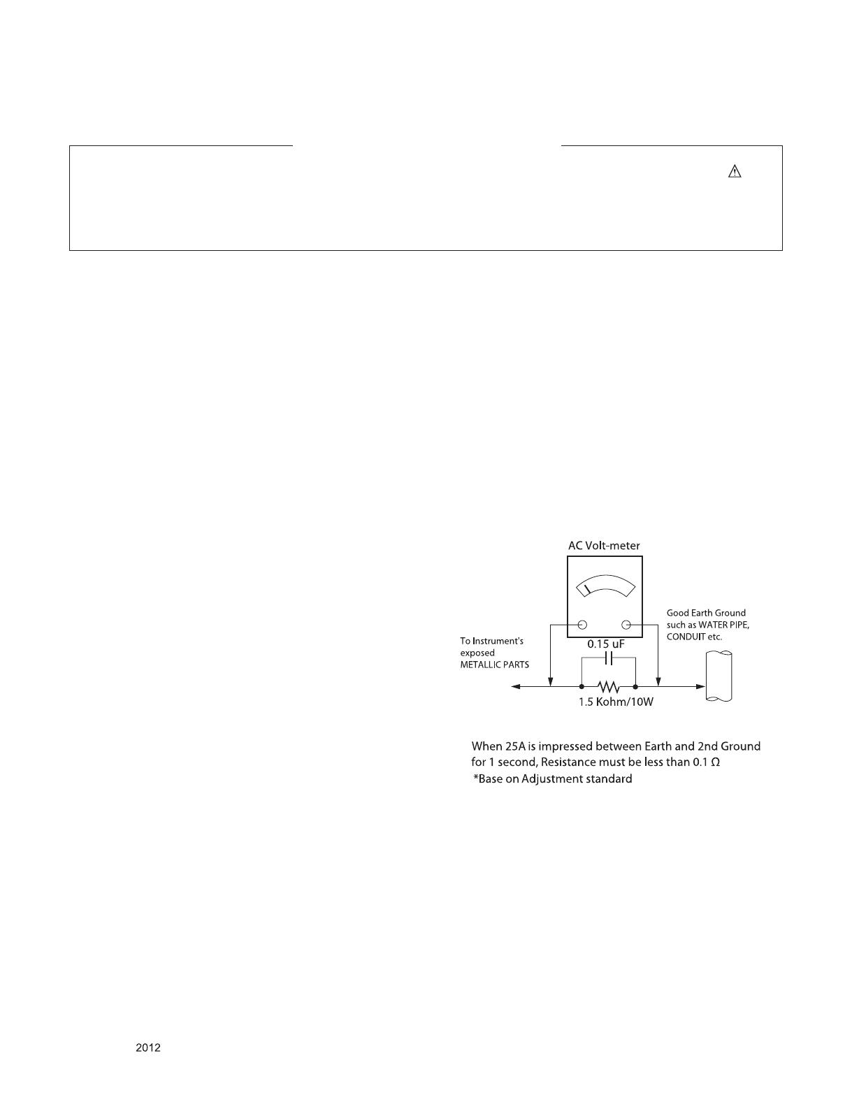
Leakage Current Hot Check (See below Figure)
Plug the AC cord directly into the AC outlet.
Do not use a line Isolation Transformer during this check.
Connect 1.5 K / 10 watt resistor in parallel with a 0.15 uF capacitor
between a known good earth ground (Water Pipe, Conduit, etc.)
and the exposed metallic parts.
Measure the AC voltage across the resistor using AC voltmeter
with 1000 ohms/volt or more sensitivity.
Reverse plug the AC cord into the AC outlet and repeat AC voltage
measurements for each exposed metallic part. Any voltage
measured must not exceed 0.75 volt RMS which is corresponds to
0.5 mA.
In case any measurement is out of the limits specified, there is
possibility of shock hazard and the set must be checked and
repaired before it is returned to the customer.
Leakage Current Hot Check circuit
IMPORTANT SAFETY NOTICE
SAFETY PRECAUTIONS

- 4 -
LGE Internal Use OnlyCopyright © LG Electronics. Inc. All rights reserved.
Only for training and service purposes
SERVICING PRECAUTIONS
CAUTION: Before servicing receivers covered by this service
manual and its supplements and addenda, read and follow the
SAFETY PRECAUTIONS on page 3 of this publication.
NOTE: If unforeseen circumstances create conict between the
following servicing precautions and any of the safety precautions
on page 3 of this publication, always follow the safety precautions.
Remember: Safety First.
General Servicing Precautions
1. Always unplug the receiver AC power cord from the AC power
source before;
a. Removing or reinstalling any component, circuit board mod-
ule or any other receiver assembly.
b. Disconnecting or reconnecting any receiver electrical plug or
other electrical connection.
c. Connecting a test substitute in parallel with an electrolytic
capacitor in the receiver.
CAUTION: A wrong part substitution or incorrect polarity
installation of electrolytic capacitors may result in an explo-
sion hazard.
2. Test high voltage only by measuring it with an appropriate
high voltage meter or other voltage measuring device (DVM,
FETVOM, etc) equipped with a suitable high voltage probe.
Do not test high voltage by "drawing an arc".
3. Do not spray chemicals on or near this receiver or any of its
assemblies.
4. Unless specied otherwise in this service manual, clean
electrical contacts only by applying the following mixture to the
contacts with a pipe cleaner, cotton-tipped stick or comparable
non-abrasive applicator; 10 % (by volume) Acetone and 90 %
(by volume) isopropyl alcohol (90 % - 99 % strength)
CAUTION: This is a ammable mixture.
Unless specied otherwise in this service manual, lubrication of
contacts in not required.
5. Do not defeat any plug/socket B+ voltage interlocks with which
receivers covered by this service manual might be equipped.
6. Do not apply AC power to this instrument and/or any of its
electrical assemblies unless all solid-state device heat sinks are
correctly installed.
7. Always connect the test receiver ground lead to the receiver
chassis ground before connecting the test receiver positive
lead.
Always remove the test receiver ground lead last.
8. Use with this receiver only the test xtures specied in this
service manual.
CAUTION: Do not connect the test xture ground strap to any
heat sink in this receiver.
Electrostatically Sensitive (ES) Devices
Some semiconductor (solid-state) devices can be damaged eas-
ily by static electricity. Such components commonly are called
Electrostatically Sensitive (ES) Devices. Examples of typical ES
devices are integrated circuits and some eld-effect transistors
and semiconductor “chip” components. The following techniques
should be used to help reduce the incidence of component dam-
age caused by static by static electricity.
1. Immediately before handling any semiconductor component or
semiconductor-equipped assembly, drain off any electrostatic
charge on your body by touching a known earth ground. Alter-
natively, obtain and wear a commercially available discharging
wrist strap device, which should be removed to prevent poten-
tial shock reasons prior to applying power to the unit under test.
2. After removing an electrical assembly equipped with ES
devices, place the assembly on a conductive surface such as
aluminum foil, to prevent electrostatic charge buildup or expo-
sure of the assembly.
3. Use only a grounded-tip soldering iron to solder or unsolder ES
devices.
4. Use only an anti-static type solder removal device. Some solder
removal devices not classied as “anti-static” can generate
electrical charges sufcient to damage ES devices.
5. Do not use freon-propelled chemicals. These can generate
electrical charges sufcient to damage ES devices.
6. Do not remove a replacement ES device from its protective
package until immediately before you are ready to install it.
(Most replacement ES devices are packaged with leads electri-
cally shorted together by conductive foam, aluminum foil or
comparable conductive material).
7. Immediately before removing the protective material from the
leads of a replacement ES device, touch the protective material
to the chassis or circuit assembly into which the device will be
installed.
CAUTION: Be sure no power is applied to the chassis or circuit,
and observe all other safety precautions.
8. Minimize bodily motions when handling unpackaged replace-
ment ES devices. (Otherwise harmless motion such as the
brushing together of your clothes fabric or the lifting of your
foot from a carpeted oor can generate static electricity suf-
cient to damage an ES device.)
General Soldering Guidelines
1. Use a grounded-tip, low-wattage soldering iron and appropriate
tip size and shape that will maintain tip temperature within the
range or 500 °F to 600 °F.
2. Use an appropriate gauge of RMA resin-core solder composed
of 60 parts tin/40 parts lead.
3. Keep the soldering iron tip clean and well tinned.
4. Thoroughly clean the surfaces to be soldered. Use a mall wire-
bristle (0.5 inch, or 1.25 cm) brush with a metal handle.
Do not use freon-propelled spray-on cleaners.
5. Use the following unsoldering technique
a. Allow the soldering iron tip to reach normal temperature.
(500 °F to 600 °F)
b. Heat the component lead until the solder melts.
c. Quickly draw the melted solder with an anti-static, suction-
type solder removal device or with solder braid.
CAUTION: Work quickly to avoid overheating the circuit
board printed foil.
6. Use the following soldering technique.
a. Allow the soldering iron tip to reach a normal temperature
(500 °F to 600 °F)
b. First, hold the soldering iron tip and solder the strand against
the component lead until the solder melts.
c. Quickly move the soldering iron tip to the junction of the
component lead and the printed circuit foil, and hold it there
only until the solder ows onto and around both the compo-
nent lead and the foil.
CAUTION: Work quickly to avoid overheating the circuit
board printed foil.
d. Closely inspect the solder area and remove any excess or
splashed solder with a small wire-bristle brush.

- 5 -
LGE Internal Use OnlyCopyright © LG Electronics. Inc. All rights reserved.
Only for training and service purposes
IC Remove/Replacement
Some chassis circuit boards have slotted holes (oblong) through
which the IC leads are inserted and then bent at against the cir-
cuit foil. When holes are the slotted type, the following technique
should be used to remove and replace the IC. When working with
boards using the familiar round hole, use the standard technique
as outlined in paragraphs 5 and 6 above.
Removal
1. Desolder and straighten each IC lead in one operation by
gently prying up on the lead with the soldering iron tip as the
solder melts.
2. Draw away the melted solder with an anti-static suction-type
solder removal device (or with solder braid) before removing
the IC.
Replacement
1. Carefully insert the replacement IC in the circuit board.
2. Carefully bend each IC lead against the circuit foil pad and
solder it.
3. Clean the soldered areas with a small wire-bristle brush.
(It is not necessary to reapply acrylic coating to the areas).
"Small-Signal" Discrete Transistor
Removal/Replacement
1. Remove the defective transistor by clipping its leads as close
as possible to the component body.
2. Bend into a "U" shape the end of each of three leads remaining
on the circuit board.
3. Bend into a "U" shape the replacement transistor leads.
4. Connect the replacement transistor leads to the corresponding
leads extending from the circuit board and crimp the "U" with
long nose pliers to insure metal to metal contact then solder
each connection.
Power Output, Transistor Device
Removal/Replacement
1. Heat and remove all solder from around the transistor leads.
2. Remove the heat sink mounting screw (if so equipped).
3. Carefully remove the transistor from the heat sink of the circuit
board.
4. Insert new transistor in the circuit board.
5. Solder each transistor lead, and clip off excess lead.
6. Replace heat sink.
Diode Removal/Replacement
1. Remove defective diode by clipping its leads as close as pos-
sible to diode body.
2. Bend the two remaining leads perpendicular y to the circuit
board.
3. Observing diode polarity, wrap each lead of the new diode
around the corresponding lead on the circuit board.
4. Securely crimp each connection and solder it.
5. Inspect (on the circuit board copper side) the solder joints of
the two "original" leads. If they are not shiny, reheat them and if
necessary, apply additional solder.
Fuse and Conventional Resistor
Removal/Replacement
1. Clip each fuse or resistor lead at top of the circuit board hollow
stake.
2. Securely crimp the leads of replacement component around
notch at stake top.
3. Solder the connections.
CAUTION: Maintain original spacing between the replaced
component and adjacent components and the circuit board to
prevent excessive component temperatures.
Circuit Board Foil Repair
Excessive heat applied to the copper foil of any printed circuit
board will weaken the adhesive that bonds the foil to the circuit
board causing the foil to separate from or "lift-off" the board. The
following guidelines and procedures should be followed whenever
this condition is encountered.
At IC Connections
To repair a defective copper pattern at IC connections use the
following procedure to install a jumper wire on the copper pattern
side of the circuit board. (Use this technique only on IC connec-
tions).
1. Carefully remove the damaged copper pattern with a sharp
knife. (Remove only as much copper as absolutely necessary).
2. carefully scratch away the solder resist and acrylic coating (if
used) from the end of the remaining copper pattern.
3. Bend a small "U" in one end of a small gauge jumper wire and
carefully crimp it around the IC pin. Solder the IC connection.
4. Route the jumper wire along the path of the out-away copper
pattern and let it overlap the previously scraped end of the
good copper pattern. Solder the overlapped area and clip off
any excess jumper wire.
At Other Connections
Use the following technique to repair the defective copper pattern
at connections other than IC Pins. This technique involves the
installation of a jumper wire on the component side of the circuit
board.
1. Remove the defective copper pattern with a sharp knife.
Remove at least 1/4 inch of copper, to ensure that a hazardous
condition will not exist if the jumper wire opens.
2. Trace along the copper pattern from both sides of the pattern
break and locate the nearest component that is directly con-
nected to the affected copper pattern.
3. Connect insulated 20-gauge jumper wire from the lead of the
nearest component on one side of the pattern break to the lead
of the nearest component on the other side.
Carefully crimp and solder the connections.
CAUTION: Be sure the insulated jumper wire is dressed so the
it does not touch components or sharp edges.
- 6 -
LGE Internal Use OnlyCopyright © LG Electronics. Inc. All rights reserved.
Only for training and service purposes
SPECIFICATION
NOTE : Specifications and others are subject to change without notice for improvement
.
1. Application range
This specification is applied to the LCD TV used LD2AY/Z
chassis.
2. Requirement for Test
Each part is tested as below without special appointment.
1) Temperature: 25 °C ± 5 °C(77 °F ± 9 °F), CST: 40 °C ± 5 °C
2) Relative Humidity: 65 % ± 10 %
3) Power Voltage
: Standard input voltage (AC 100-240 V~, 50/60 Hz)
* Standard Voltage of each products is marked by models.
4) Specification and performance of each parts are followed
each drawing and specification by part number in
accordance with BOM.
5) The receiver must be operated for about 5 minutes prior to
the adjustment.
3. Test method
1) Performance: LGE TV test method followed
2) Demanded other specification
- Safety : CE, IEC specification
- EMC : CE, IEC
4. Model General Specification
No. Item Specication Remarks
1 Market EU(PAL Market-37Countries) DTV & Analog (Total 36 countries)
DTV (MPEG2/4, DVB-T) :37 countries
UK/Italy/Germany/France/Spain/Sweden/Finland/Nether-
lands/ Belgium/Luxemburg/ Greece/Denmark/Czech/
Austria /Hungary/Swiss/Croatia/Turkey
Norway/Slovenia/Poland/Ukraine/Portugal/Ireland/Morocco/
Latvia/Estonia/Lithania/Rumania/Bulgaria/Russia/Slovakia
Bosnia/Serbia/Albania/Kazakhstan/Belarus
DTV (MPEG2/4, DVB-C): 37 countries
UK/Italy/Germany/France/Spain/Sweden/Finland/Nether-
lands/ Belgium/Luxemburg/ Greece/Denmark/Czech/
Austria /Hungary/Swiss/Croatia/Turkey
Norway/Slovenia/Poland/Ukraine/Portugal/Ireland/Morocco/
Latvia/Estonia/Lithania/Rumania/Bulgaria/Russia/Slovakia
Bosnia/Serbia/Albania/Kazakhstan/Belarus
2. Broadcasting system 1) PAL-BG
2) PAL-DK
3) SECAM L/L’
4) DVB-T//C
3 Receiving system Analog : Upper Heterodyne
Digital : COFDM , QAM
► DVB-T
- Guard Interval(Bitrate_Mbit/s)
1/4, 1/8, 1/16, 1/32
- Modulation : Code Rate
QPSK : 1/2, 2/3, 3/4, 5/6, 7/8
16-QAM : 1/2, 2/3, 3/4, 5/6, 7/8
64-QAM : 1/2, 2/3, 3/4, 5/6, 7/8
► DVB-C
- Symbolrate :
4.0Msymbols/s to 7.2Msymbols/s
- Modulation :
16QAM, 64-QAM, 128-QAM and 256-QAM
4 Scart Jack (1EA) PAL, SECAM Scart 1 Jack is Full scart and
support RF-OUT(analog).
5 Component Input (1EA) Y/Cb/Cr
Y/Pb/Pr
- 7 -
LGE Internal Use OnlyCopyright © LG Electronics. Inc. All rights reserved.
Only for training and service purposes
No. Item Specication Remarks
6 RGB Input RGB-PC Analog(D-SUB 15PIN)
7 HDMI Input (3EA)
HDMI1-DTV/DVI
HDMI2-DTV
HDMI3-DTV
PC(HDMI version 1.3)
Support HDCP
The number of Input ports is different by model.
8 Audio Input (2EA) RGB/DVI Audio In case of the RGB/DVI Audio input,
9 SDPIF out (1EA) SPDIF out Some models(LD21A,LD21C) are not supported.
10 Earphone out (1EA)
Antenna, AV1, AV2, Component, RGB,
HDMI1, HDMI2, HDMI3
.
11 USB (1EA )
EMF,
DivX HD,
For SVC (download)
JPEG, MP3, DivX HD
12 DVB
DVB-T
CI : UK, Finland, Denmark, Norway, Sweden, Russia,
Spain, Ireland, Luxemburg, Belgium, Netherland
CI+ : France(Canal+), Italy(DGTVi)
DVB-C
CI : Switzerland, Austria, Slovenia, Hungary, Bulgaria
CI+ : Switzerland(UPC,Cablecom), Netherland(Ziggo),
Germany(KDG,CWB), Finland(labwise)
13 RS232C (1EA) Interactive mode support

- 8 -
LGE Internal Use OnlyCopyright © LG Electronics. Inc. All rights reserved.
Only for training and service purposes
5. Video resolutions (2D)
5.1. Component Input (Y, CB/PB, CR/PR)
5.2. RGB Input (PC)
No. Resolution H-freq(kHz) V-freq(Hz) Pixel clock(MHz) Proposed
1 720*480 15.73 60.00 13.5135 SDTV ,DVD 480I
2 720*480 15.73 59.94 13.50 SDTV ,DVD 480I
3 720*480 31.50 60.00 27.027 SDTV 480P
4 720*480 31.47 59.94 27.00 SDTV 480P
5 1280*720 45.00 60.00 74.25 HDTV 720P
6 1280*720 44.96 59.94 74.176 HDTV 720P
7 1920*1080 33.75 60.00 74.25 HDTV 1080I
8 1920*1080 33.72 59.94 74.176 HDTV 1080I
9 1920*1080 67.50 60.00 148.50 HDTV 1080P
10 1920*1080 67.432 59.94 148.352 HDTV 1080P
11 1920*1080 27.00 24.00 74.25 HDTV 1080P
12 1920*1080 26.97 23.94 74.176 HDTV 1080P
13 1920*1080 33.75 30.00 74.25 HDTV 1080P
14 1920*1080 33.71 29.97 74.176 HDTV 1080P
No. Resolution H-freq(kHz) V-freq.(Hz) Pixel clock(MHz) Proposed DDC
1 640*350 31.468 70.09 25.17 EGA X
2 720*400 31.469 70.08 28.32 DOS O
3 640*480 31.469 59.94 25.17 VESA(VGA) O
4 800*600 37.879 60.31 40.00 VESA(SVGA) O
5 1024*768 48.363 60.00 65.00 VESA(XGA) O
6 1280*768 47.776 59.870 79.50 VESA O
7 1360*768 47.712 60.015 85.50 VESA (WXGA) O
8 1280*1024 63.981 60.020 108.0 HDTV 1080P O
9 1600*1200 75.00 60.00 162.0
10 1920*1080 66.587 59.934 138.5

- 9 -
LGE Internal Use OnlyCopyright © LG Electronics. Inc. All rights reserved.
Only for training and service purposes
5.3. HDMI Input(PC/DTV)
No. Resolution H-freq(kHz) V-freq.(Hz) Pixel clock(MHz) Proposed Remark
PC(DVI) DDC
1 640*350 31.468 70.09 25.17 EGA X
2 720*400 31.469 70.08 28.32 DOS O
3 640*480 31.469 59.94 25.17 VESA(VGA) O
4 800*600 37.879 60.31 40.00 VESA(SVGA) O
5 1024*768 48.363 60.00 65.00 VESA(XGA) O
6 1280*768 47.776 59.870 79.50 CVT(WXGA) Х
7 1360*768 47.712 60.015 85.50 VESA (WXGA) O
8 1280*1024 63.981 60.020 108.0 VESA (SXGA) O
9 1600*1200 75.00 60.00 162.0 VESA (UXGA) X
10 1920*1080 67.50 60.00 148.5 HDTV 1080P O
DTV
1 720*480 31.50 60.00 27.027 SDTV 480P
2 720*480 31.47 59.94 27.00 SDTV 480P
3 1280*720 45.00 60.00 74.25 HDTV 720P
4 1280*720 44.96 59.94 74.176 HDTV 720P
5 1920*1080 33.75 60.00 74.25 HDTV 1080I
6 1920*1080 33.72 59.94 74.176 HDTV 1080I
7 1920*1080 67.50 60.00 148.50 HDTV 1080P
8 1920*1080 67.432 59.94 148.352 HDTV 1080P
9 1920*1080 27.00 24.00 74.25 HDTV 1080P
10 1920*1080 26.97 23.976 74.176 HDTV 1080P
11 1920*1080 33.75 30.00 74.25 HDTV 1080P

- 10 -
LGE Internal Use OnlyCopyright © LG Electronics. Inc. All rights reserved.
Only for training and service purposes
ADJUSTMENT INSTRUCTION
1. Application Range
This specification sheet is applied to all of the LCD TV with
LD2AY/Z chassis.
2. Designation
(1) The adjustment is according to the order which is designated
and which must be followed, according to the plan
which
can be changed only on agreeing.
(2) Power adjustment : Free Voltage.
(3) Magnetic Field Condition: Nil.
(4) Input signal Unit: Product Specification Standard.
(5) Reserve after operation : Above 5 Minutes (Heat Run)
Temperature : at 25 °C ± 5 °C
Relative humidity : 65 ± 10 %
Input voltage : 220 V, 60 Hz
(6) Adjustment equipments: Color Analyzer(CA-210 or CA-110),
DDC Adjustment Jig, Service remote control.
(7) Push the "IN STOP" key - For memory initialization.
3. Main PCB check process
▪ APC - After Manual-Insert, executing APC
* Boot file Download
(1) Execute ISP program "Mstar ISP Utility" and then click
"Config" tab.
(2) Set as below, and then click "Auto Detect" and check "OK"
message.
If "Error" is displayed, check connection between computer,
jig, and set.
(3) Click "Read" tab, and then load download file(XXXX.bin)
by clicking "Read"
(4) Click "Connect" tab. If "Can't" is displayed, check connection
between computer, jig, and set.
(5) Click "Auto" tab and set as below.
(6) Click "Run".
(7) After downloading, check "OK" message.
* USB DOWNLOAD
(1) Put the USB Stick to the USB socket.
(2) Automatically detecting update file in USB Stick.
- If your downloaded program version in USB Stick is Low,
it didn't work. But your downloaded version is High, USB
data is automatically detecting.
(3) Show the message "Copying files from memory".
(4) Updating is starting.
(5) Updating Completed, The TV will restart automatically.
(6) If your TV is turned on, check your updated version and
Tool option. (explain the Tool option, next stage)
* If downloading version is more high than your TV have, TV
can lost all channel data. In this case, you have to channel
recover. if all channel data is cleared, you didn’t have a DTV/
ATV test on production line.
* After downloading, have to adjust Tool Option again.
(1) Push "IN-START" key in service remote control.
(2) Select "Tool Option 1" and push "OK" key.
(3) Punch in the number. (Each model has their number)
(1)
filexxx.bin
(4)
(5)
(6)
(7)...........OK
filexxx.bin
(2)
(3)
Please Check the Speed :
To use speed between
from 200KHz to 400KHz
Case1 : Software version up
1. After downloading S/W by USB , TV set will reboot
automatically.
2. Push “In-stop” key.
3. Push “Power on” key.
4. Function inspection
5. After function inspection, Push “In-stop” key.
Case2 : Function check at the assembly line
1. When TV set is entering on the assembly line, Push
“In-stop” key at rst.
2. Push “Power on” key for turning it on.
→ If you push “Power on” key, TV set will recover
channel information by itself.
3. After function inspection, Push “In-stop” key.
- 11 -
LGE Internal Use OnlyCopyright © LG Electronics. Inc. All rights reserved.
Only for training and service purposes
3.1. ADC Process
(1) ADC
- Enter Service Mode by pushing "ADJ" key,
- Enter Internal ADC mode by pushing "►" key at "7. ADC
Calibration".
<Caution> Using "P-ONLY" key of the Adjustment remote
control, power on TV.
If there is no Component Input, disappear “ADC Comp” message.
* ADC Calibration Protocol (RS232)
Adjust Sequence
▪ aa 00 00 [Enter Adjust Mode]
▪ xb 00 40 [Component1 Input (480i)]
▪ ad 00 10 [Adjust 480i Comp1]
▪ xb 00 60 [RGB Input (1024*768)] (only LD21B)
▪ ad 00 10 [Adjust 1024*768 RGB] (only LD21B)
▪ aa 00 90 End Adjust mode
* Required equipment : Adjustment remote control.
3.2. Function Check
3.2.1. Check display and sound
■ Check Input and Signal items. (cf. work instructions)
1. TV
2. AV
3. COMPONENT (480i)
4. RGB (PC : 1024 x 768 @ 60hz)
5. HDMI
6. PC Audio In
* Display and Sound check is executed by Remote controller
Caution : Not to push the INSTOP KEY after completion if the
function inspection.
4. Total Assembly line process
4.1. Adjustment Preparation
▪ W/B Equipment condition
CA210
: CCFL/EEFL -> CH9, Test signal: Inner pattern(80IRE)
LED -> CH14, Test signal: Inner pattern(80IRE)
▪ Above 5 minutes H/run in the inner pattern. (“power on” key
of adjust remote control)
▪ Edge LED W/B Table in process of aging time (Only LGD
Edge LED Module except AUO, CMI, IPS Module)
CA210 : CH 14, Test signal : Inner pattern (80IRE)
* Connecting picture of the measuring instrument
(On Automatic control)
Inside PATTERN is used when W/B is controlled. Connect to
auto controller or push Adjustment R/C POWER ON →
Enter the mode of White-Balance, the pattern will come out.
* Auto-control interface and directions
(1) Adjust in the place where the influx of light like floodlight
around is blocked. (illumination is less than 10 lux).
(2) Adhere closely the Color analyzer(CA210) to the module
less than 10 cm distance, keep it with the surface of the
Module and Color analyzer's prove vertically.(80° ~ 100°).
(3) Aging time
- After aging start, keep the power on (no suspension of
power supply) and heat-run over 5 minutes.
- Using 'no signal' or 'POWER ONLY' or the others, check
the back light on.
EZ ADJUST
0. Tool Option1
1. Tool Option2
2
. Tool Option3
3
. Tool Option4
4
. Tool Option 5
5
. Country Group
6. Area Option
7
. ADC Calibration ඖ
8. White Balance
9
. 10 Point WB
10
. Test Pattern
1
1. EDID D/L
1
2. Sub B/C
1
3. Touch Sensitivity Setting
ADC Calibration
ADC Comp 480i NG
ADC Comp 1080p NG
ADC RGB NG
Start Reset
NO Item CMD 1 CMD 2 Data 0
Enter
Adjust MODE
Adjust
‘Mode In’
A A 0 0
When transfer the ‘Mode In’,
Carry the command.
ADC adjust ADC Adjust A D 1 0
Automatically adjustment
(The use of a internal pattern)
GP4
Aging
time
(Min)
Cool Medium Warm
X y x y x y
269 273 285 293 313 329
1 0-2 279 288 295 308 319 338
2 3-5 278 286 294 306 318 336
3 6-9 277 285 293 305 317 335
4 10-19 276 283 292 303 316 333
5 20-35 274 280 290 300 314 330
6 36-49 272 277 288 297 312 327
7 50-79 271 275 287 295 311 325
8 80-149 270 274 286 294 310 324
9 Over 150 269 273 285 293 309 323
Full White Pattern
CA-210
COLOR
ANALYZER
TYPE : CA-210
RS-232C Communication
Mode Temp Coordinate spec
Cool 13,000k
X=0.269 (±0.002)
Y=0.273 (±0.002)
<Test Signal>
Inner pattern
(204gray,
80IRE)
Medium 9,300k
X=0.285 (±0.002)
Y=0.293 (±0.002)
Warm 6,500k
X=0.313 (±0.002)
Y=0.329 (±0.002)

- 12 -
LGE Internal Use OnlyCopyright © LG Electronics. Inc. All rights reserved.
Only for training and service purposes
▪ Auto adjustment Map(using RS-232C to USB cable)
RS-232C COMMAND
[CMD ID DATA]
Wb 00 00 White Balance Start
Wb 00 ff White Balance End
<Caution>
Color Temperature : COOL, Medium, Warm.
One of R Gain/G Gain/ B Gain should be kept on 0xC0, and
adjust other two lower than C0.(When R/G/B Gain are all
C0, it is the FULL Dynamic Range of Module)
* Manual W/B process using adjust Remote control.
▪ After enter Service Mode by pushing "ADJ" key,
▪ Enter White Balance by pushing "
►
" key at "8. White
Balance".
* After you finished all adjustments, Press "In-start" key and
compare Tool option and Area option value with its BOM, if
it is correctly same then unplug the AC cable. If it is not
same, then correct it same with BOM and unplug AC cable.
For correct it to the model's module from factory Jig model.
* Push the "IN STOP" key after completing the function
inspection. And Mechanical Power Switch must be set “ON”.
4.2. DDC EDID Write (RGB 128Byte )
■ Connect D-sub Signal Cable to D-Sub Jack.
■ Write EDID DATA to EEPROM (24C02) by using DDC2B
protocol.
■ Check whether written EDID data is correct or not.
* For Service main Assembly, EDID have to be downloaded to
Insert Process in advance.
4.3 DDC EDID Write (HDMI 256Byte)
■ Connect HDMI Signal Cable to HDMI Jack.
■ Write EDID DATA to EEPROM(24C02) by using DDC2B
protocol.
■ Check whether written EDID data is correct or not.
* For Service main Assembly, EDID have to be downloaded to
Insert Process in advance.
4.4. EDID data
(1) All Data : HEXA Value
(2) Changeable Data :
*: Serial No : Controlled / Data:01
**: Month : Controlled / Data:00
***:Year : Controlled
****:Check sum
4.4.1. Auto Download
■ After enter Service Mode by pushing “ADJ” key,
■Enter EDID D/L mode.
■Enter “START” by pushing “OK” key.
* Caution : Never connect HDMI & D-sub Cable when EDID
downloaded.
* EDID data and Model option download (RS232)
4.4.2. Manual Download
<Caution>
(1) Use the proper signal cable for EDID Download
- Analog EDID : Pin3 exists
- Digital EDID : Pin3 exists
(2) Never connect HDMI & D-sub Cable at the same time.
(3) Use the proper cables below for EDID Writing.
(4) Download HDMI1, HDMI2 separately because HDMI1 is
different from HDMI2.
RS-232C COMMAND
[CMD ID DATA]
MIN
CENTER
(DEFAULT)
MAX
Cool Mid Warm Cool Mid Warm
R Gain jg Ja jd 00 172 192 192 192
G Gain jh Jb je 00 172 192 192 192
B Gain ji Jc jf 00 192 192 172 192
R Cut 64 64 64 128
G Cut 64 64 64 128
B Cut 64 64 64 128
EZ ADJUST
0. Tool Option1
1. Tool Option2
2. Tool Option3
3. Tool Option4
4. Tool Option5
5. Country Group
6. Area Option
7. ADC Calibration
8. White Balance ►
9. 10 Point WB
10. Test Pattern
11. EDID D/L
12. Sub B/C
13. Touch Sensitivity Setting
White Balance
Color Temp.
R-Gain
G-Gain
B-Gain
R-Cut
G-Cut
B-Cut
Test-Pattern
Backlight
Reset
Cool
172
172
192
64
64
64
ON
100
To Set
lGhkq|z{G
WUG{GvXG
X
UG{GvYG
Y
UG{GvZG
Z
UG{Gv[G
[
UG{Gv\G
\
UG{GvGjG
]
UGjGnG
^
UGhGvG
_
UGhkjGjG
`
UG~GiG
X
WUGXWGwG~iG
X
XUG{GwG
X
YGlkpkGkVsG ඖ
XZ zGiVjG
X
[UGlUGpGhG
l
kpkGkVsG
o
ktpXG unG
o
ktpYG unG
o
ktpZG unG
y
niG unG
zG yG
lkpkGkVsG
o
ktpXG vrG
o
ktpYG vrG
o
ktpZG vrG
y
niG vrG
zG yG
NO Item CMD 1 CMD 2 Data 0
Enter download
MODE
Download
‘Mode In’
A A 0 0
When transfer the ‘Mode
In’, Carry the command.
EDID data and
Model option
download
Download A E 00 10
Automatically download
(The use of a internal
data)
For Analog For HDMI EDID
D-sub to D-sub DVI-D to HDMI or HDMI to HDMI
No. Item Condition Hex Data
1 Manufacturer ID GSM 1E6D
2 Version Digital : 1 01
3 Revision Digital : 3 03

- 13 -
LGE Internal Use OnlyCopyright © LG Electronics. Inc. All rights reserved.
Only for training and service purposes
(1) FHD RGB EDID data
(2) FHD HDMI EDID data
(3) Detail EDID Options are below
a. Product ID
b. Serial No: Controlled on production line.
c. Month, Year: Controlled on production line:
ex) Week : '01' -> '01'
Year : '2012' -> '16' fix
d. Model Name(Hex):
cf) TV set’s model name in EDID data is below.
e. Checksum: Changeable by total EDID data.
f. Vendor Specific(HDMI)
4.5. Outgoing condition Configuration
■ When pressing IN-STOP key by SVC remocon, Red LED
are blinked alternatively. And then automatically turn off.
(Must not AC power OFF during blinking)
4.6. HI-POT Test
4.6.1. HI-POT auto-check preparation
- Check the POWER cable and SIGNAL cable insertion condition
4.6.2. HI-POT auto-check
(1) Pallet moves in the station. (POWER CORD / AV CORD is
tightly inserted)
(2) Connect the AV JACK Tester.
(3) Controller (GWS103-4) on.
(4) HI-POT test (Auto)
- If Test is failed, Buzzer operates.
- If Test is passed, GOOD Lamp on and move to next proc-
ess automatically.
4.6.3. Checkpoint
(1) Test voltage
- Touchable Metal : 3 KV / min at 100 mA
- SIGNAL : 3 KV / min at 100 mA
(2) TEST time: 1 second. (case : mass production )
(3) TEST POINT
- Touchable Metal => LIVE & NEUTRAL : Touchable Metal.
- SIGNAL => LIVE & NEUTRAL : SIGNAL.
0 1 2 3 4 5 6 7 8 9 A B C D E F
00 00 FF FF FF FF FF FF 00 1E 6D a b
10 c 01 03 68 A0 5A 78 0A EE 91 A3 54 4C 99 26
20 0F 50 54 A1 08 00 31 40 45 40 61 40 71 40 81 80
30 01 01 01 01 01 01 02 3A 80 18 71 38 2D 40 58 2C
40 45 00 A0 5A 00 00 00 1E 66 21 50 B0 51 00 1B 30
50 40 70 36 00 A0 5A 00 00 00 1E 00 00 00 FD 00 3A
60 3E 1E 53 10 00 0A 20 20 20 20 20 20 d
70 d 00 e
0 1 2 3 4 5 6 7 8 9 A B C D E F
00 00 FF FF FF FF FF FF 00 1E 6D a b
10 c 01 03 80 A0 5A 78 0A EE 91 A3 54 4C 99 26
20 0F 50 54 A1 08 00 31 40 45 40 61 40 71 40 81 80
30 01 01 01 01 01 01 02 3A 80 18 71 38 2D 40 58 2C
40 45 00 A0 5A 00 00 00 1E 66 21 50 B0 51 00 1B 30
50 40 70 36 00 A0 5A 00 00 00 1E 00 00 00 FD 00 3A
60 3E 1E 53 10 00 0A 20 20 20 20 20 20 d
70 d 01 e
80 02 03 22 F1 4E 10 9F 04 13 05 14 03 02 12 20 21
90 22 15 01 26 15 07 50 09 57 07 f
A0 f 01 1D 80 18 71 1C 16 20 58 2C 25 00 20 C2
B0 31 00 00 9E 01 1D 00 72 51 D0 1E 20 6E 28 55 00
C0 20 C2 31 00 00 1E 02 3A 80 18 71 38 2D 40 58 2C
D0 45 00 A0 5A 00 00 00 1E 01 1D 00 BC 52 D0 1E 20
E0 B8 28 55 40 C4 8E 21 00 00 1E 00 00 00 00 00 00
F0 00 00 00 00 00 00 00 00 00 00 00 00 00 00 00 e
MODEL NAME HEX EDID Table DDC Function
HD/FHD Model 0001 01 00 Analog/Digital
Model name MODEL NAME(HEX)
LG TV 00 00 00 FC 00 4C 47 20 54 56 0A 20 20 20 20 20 20 20 (LG TV)
EDID C/S data
HD
HDMI RGB
Check sum
(Hex)
Block 0 43 5C
Block 1
25 (HDMI1)
-15 (HDMI2)
5 (HDMI3)
Input Model name(HEX)
HDMI1 67030C001000B82D
HDMI2 67030C002000B82D
HDMI3 67030C003000B82D
- 14 -
LGE Internal Use OnlyCopyright © LG Electronics. Inc. All rights reserved.
Only for training and service purposes
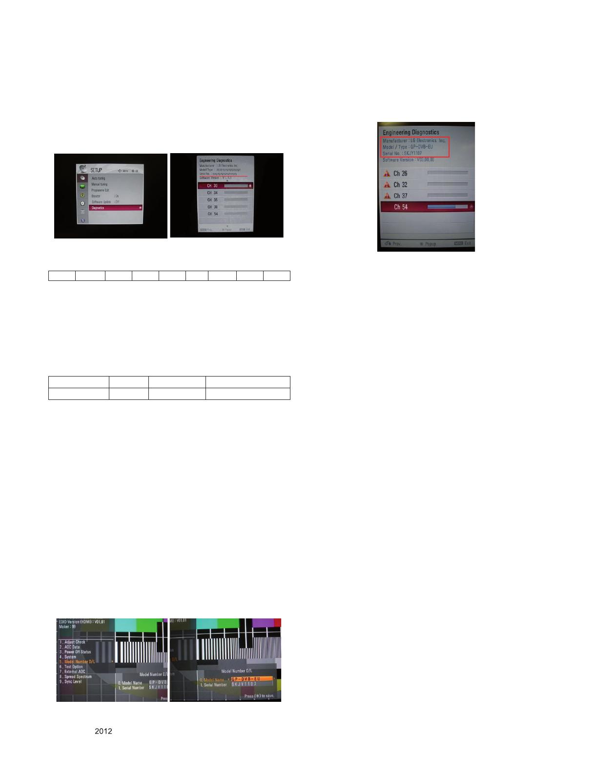
5. Model name & Serial number D/L
▪ Press "Power on" key of service remote control.
(Baud rate : 115200 bps)
▪ Connect RS232 Signal Cable to RS-232 Jack.
▪ Write Serial number by use RS-232.
▪ Must check the serial number at the Product/Service info..
(menu key -> red key -> select product/Service info)
5.1. Signal Table
CMD : A0h
LENGTH : 85~94h (1~16 bytes)
ADH : EEPROM Sub Address high (00~1F)
ADL : EEPROM Sub Address low (00~FF)
Data : Write data
CS : CMD + LENGTH + ADH + ADL + Data_1 +...+ Data_n
Delay : 20ms
5.2. Comand Set
* Description
FOS Default write : <7mode data> write
Vtotal, V_Frequency, Sync_Polarity, Htotal, Hstart, Vstart, 0,
Phase
Data write : Model Name and Serial Number write in EEPROM,.
5.3. Method & notice
(1) Serial number D/L is using of scan equipment.
(2) Setting of scan equipment operated by Manufacturing
Technology Group.
(3) Serial number D/L must be conformed when it is produced in
production line, because serial number D/L is mandatory by
D-book 4.0.
* Manual Download(Model Name and Serial Number)
If the TV set is downloaded by OTA or Service man, sometimes
model name or serial number is initialized.(Not always)
There is impossible to download by bar code scan, so It need
Manual download.
1) Press the "Instart" key of Adjustment remote control.
2) Go to the menu "6.Model Number D/L" like below photo.
3) Input the Factory model name or Serial number like photo.
4) Check the model name Instart menu.
→
Factory name displayed.
(ex 42LD450-ZA)
5) Check the Diagnostics.(DTV country only) → Buyer model
displayed.(ex 42LD450)
CMD LENGTH ADH ADL DATA_1 . . . Data_n CS DELAY
Adjust mode CMD(hex) LENGTH(hex) Description
EEPROM WRITE A0h 84h+n n-bytes Write (n = 1~16)

- 15 -
LGE Internal Use OnlyCopyright © LG Electronics. Inc. All rights reserved.
Only for training and service purposes
6. CI+ Key Download method
6.1. Download Procedure
(1) Press "Power on" key of a service R/C.
(Baud rate : 115200 bps)
(2) Connect RS232-C Signal Cable.
(3) Write CI+ Key through RS-232-C.
(4) Check whether the key was downloaded or not at ‘In Start’
menu. (Refer to below).
=> Check the Download to CI+ Key value in LGset.
1. Check the method of CI+ Key value
a. Check the method on Instart menu
b. Check the method of RS232C Command
1) Into the main ass’y mode (RS232 : aa 00 00)
2) Check the key download for transmitted command
(RS232 : ci 00 10)
3) Result value
- Normally status for download : OKx
- Abnormally status for download : NGx
2. Check the method of CI+ key value (RS232)
1) Into the main ass’y mode (RS232 : aa 00 00)
2) Check the mothed of CI+ key by command
(RS232 : ci 00 20)
3) result value
i 01 OK 1d1852d21c1ed5dcx
CMD 1 CMD 2 Data 0
A A 0 0
CMD 1 CMD 2 Data 0
C I 1 0
CMD 1 CMD 2 Data 0
A A 0 0
CMD 1 CMD 2 Data 0
C I 2 0
CI
+ Key Value
- 16 -
LGE Internal Use OnlyCopyright © LG Electronics. Inc. All rights reserved.
Only for training and service purposes
F -SCART
IF_N/P_MSTAR
NAND Flash
(NTP7000)
Pb
SC1_CVBS/R/G/B/FB_IN
I2S
Tuner
PCM_A[0:7]
TU_CVBS
PCM_A[0:7]
DDR3 (1GB)
IC1202
B_TMDQ[0:16]
USB Power
SC1_L/R_IN, E_AM_AUDIO,AV_L/R_IN,
COMP_L/R_IN, PC_L/R_IN
Head
Phone
232C
SPDIF
SPDIF_OUT
HP_L/ROUT
L/R
PI_TS_DATA[0:7]
FE_TS_DATA[0:7]
CI_ADDR[0:7]
AUDIO IN
NEC_TX/RX
HPD1/2, HDMI_CEC, 5V_HDMI 1/2/3
TMDS[0:7] ( Data, Clock (+/-))
USB_DM/DP
EEPROM
I2C
LVDS (8bit or 10 bit)
Serial Flash
DC/DC Conv.
(12V to 5V)
5V
12V
Power SW
(12V On/Off)
uPD78F1164A
LED Driver
I2C SW
I2C
I2C
MST_TX/RX
LED Clock
Speaker Out
Audio amp
Speaker Out
Control
Up/Down
TU_SIF
CI_TS_DATA[0:7]
RGB
COMPONENT
-
NAND01GW3B2CN6E
Digital amp
COMP_Y/ /Pr
DSUB_ R/G/B
CI Slot
Buffer
DDR3 (1GB)
IC1202
TV/DTV_VOUT
A_TMDQ[0:16]
RS-
EEPROM
M24M01
CAT24WC08W
For Boot
HDMI 1/2/3
MP2305
MP5000
12V
NEC Micom
(TPA6011A4PWPRG4)
L/R_BTL
74LVC16244
Buffer
S7LR
X-tal
24M
51P
30P
MX25L8006EM2I
DDR3 (1GB)
IC1202
SPDIF_OUT
L/R
NEC_TX/RX
12V
(IC1102)
DDR3 (2GB)
DSUB_ R/G/B
DDR3 (1GB)
IC1202
AOZ1073AIL-3
USB Power
MAX3232CDR
12V
S7LR
IC1201
Half
NIM
(CAN)
--
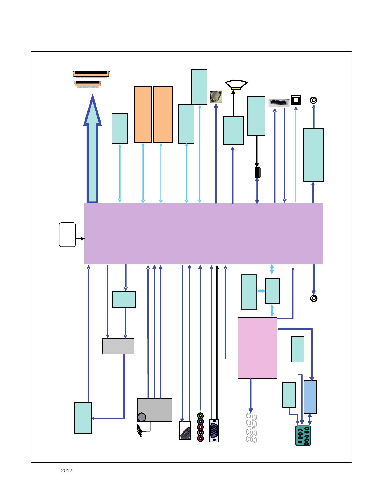
BLOCK DIAGRAM
- 17 -
LGE Internal Use OnlyCopyright © LG Electronics. Inc. All rights reserved.
Only for training and service purposes
LV1
300
200
540
521
530
550
810
820
120
500
501
510
400
900
910
A2
A4
A10
* Set + Stand
* Stand Base + Body
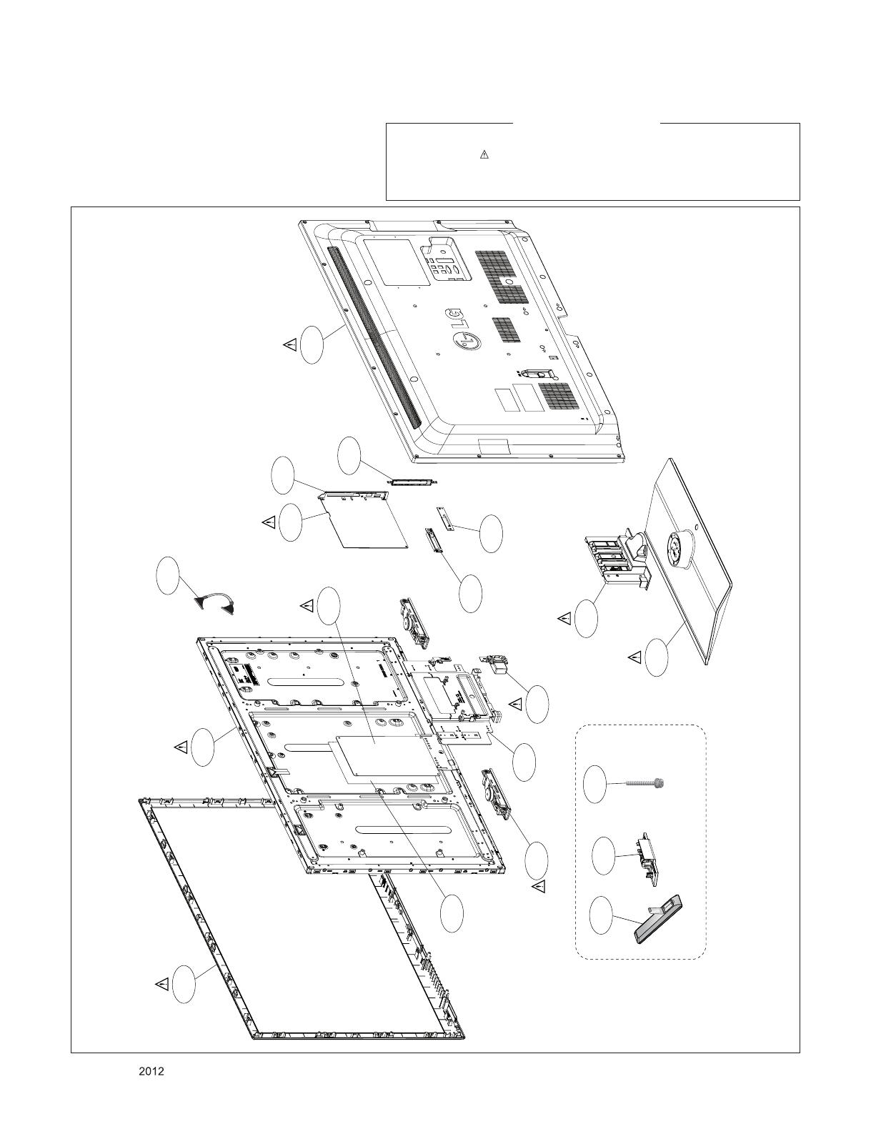
EXPLODED VIEW
Many electrical and mechanical parts in this chassis have special safety-related characteristics. These
parts are identified by in the Schematic Diagram and EXPLODED VIEW.
It is essential that these special safety parts should be replaced with the same components as
recommended in this manual to prevent X-RADIATION, Shock, Fire, or other Hazards.
Do not modify the original design without permission of manufacturer.
IMPORTANT SAFETY NOTICE

THE SYMBOL MARK OF THIS SCHEMETIC DIAGRAM INCORPORATES
SPECIAL FEATURES IMPORTANT FOR PROTECTION FROM X-RADIATION.
FILRE AND ELECTRICAL SHOCK HAZARDS, WHEN SERVICING IF IS
ESSENTIAL THAT ONLY MANUFATURES SPECFIED PARTS BE USED FOR
THE CRITICAL COMPONENTS IN THE SYMBOL MARK OF THE SCHEMETIC.
/PCM_IOWR
8pF
OPT
C106
/PCM_CD
/PCM_WE
22
R111
5V_DET_HDMI_4
22R142
OPT
100pF
50V
C112
OPT
0.1uF
OPT
C108
AMP_SCL
1K
R117
OPT
EEPROM_SDA
33R146
PWM0
/PF_WP
10K
R132
SENSOR_SDA
RGB_DDC_SDA
DSUB_DET
RXB0+
FE_TS_VAL_ERR
PCM_RST
1K
R165
NAND01GW3B2CN6E
EAN60762401
IC102
NAND_FLASH_1G_NUMONYX
26
NC_17
27
NC_18
28
NC_19
29
I/O0
30
I/O1
31
I/O2
32
I/O3
33
NC_20
34
NC_21
35
NC_22
36
VSS_2
37
VDD_2
38
NC_23
39
NC_24
40
NC_25
41
I/O4
42
I/O5
43
I/O6
44
I/O7
45
NC_26
46
NC_27
47
NC_28
48
NC_29
17
AL
3
NC_3
6
NC_6
16
CL
15
NC_10
14
NC_9
13
VSS_1
12
VDD_1
11
NC_8
10
NC_7
9
E
8
R
7
RB
4
NC_4
5
NC_5
25
NC_16
24
NC_15
23
NC_14
2
NC_2
22
NC_13
21
NC_12
1
NC_1
20
NC_11
19
WP
18
W
I2C_SDA
RXB3-
4.7K
R127
HDCP_EEPROM
1K
R141
AV_CVBS_DET
PI_TS_DATA[0-7]
H27U1G8F2BTR-BC
EAN35669102
IC102-*1
NAND_FLASH_1G_HYNIX
26
NC_17
27
NC_18
28
NC_19
29
I/O0
30
I/O1
31
I/O2
32
I/O3
33
NC_20
34
NC_21
35
NC_22
36
VSS_2
37
VCC_2
38
NC_23
39
NC_24
40
NC_25
41
I/O4
42
I/O5
43
I/O6
44
I/O7
45
NC_26
46
NC_27
47
NC_28
48
NC_29
17
ALE
3
NC_3
6
NC_6
16
CLE
15
NC_10
14
NC_9
13
VSS_1
12
VCC_1
11
NC_8
10
NC_7
9
CE
8
RE
7
R/B
4
NC_4
5
NC_5
25
NC_16
24
NC_15
23
NC_14
2
NC_2
22
NC_13
21
NC_12
1
NC_1
20
NC_11
19
WP
18
WE
/PF_CE1
EEPROM_SDA
RXA4-
33R151
56
R148
1K
R115
OPT
TC58NVG0S3ETA0BBBH
EAN61508001
IC102-*3
NAND_FLASH_1G_TOSHIBA
26
NC_17
27
NC_18
28
NC_19
29
I/O1
30
I/O2
31
I/O3
32
I/O4
33
NC_20
34
NC_21
35
NC_22
36
VSS_2
37
VCC_2
38
NC_23
39
NC_24
40
NC_25
41
I/O5
42
I/O6
43
I/O7
44
I/O8
45
NC_26
46
NC_27
47
NC_28
48
NC_29
17
ALE
3
NC_3
6
NC_6
16
CLE
15
NC_10
14
NC_9
13
VSS_1
12
VCC_1
11
NC_8
10
NC_7
9
CE
8
RE
7
RY/BY
4
NC_4
5
NC_5
25
NC_16
24
NC_15
23
NC_14
2
NC_2
22
NC_13
21
NC_12
1
NC_1
20
NC_11
19
WP
18
WE
/FLASH_WP
22
AR103
22R154
OPT
MST_NEC_TX
RGB_DDC_SCL
1K
R140
1K
R121
OPT
+3.3V_Normal
USB1_CTL
EEPROM_SCL
/PCM_IORD
HP_DET
PI_TS_CLK
22R129
HDCP_EEPROM
1K
R107
PCM_A[0-7]
RXA2+
22R114
OPT
RXACK-
RXA3+
/CI_CD2
/PCM_CE
AMP_SDA
RXA0-
FE_TS_DATA[0-7]
2.2K
R145
10K
R104
OPT
PCM_A[0-14]
PWM1
RXA1-
RXA4+
RXB2-
USB1_OCD
PWM_DIM
22R166
OPT
22R137
1K
R118
/PF_OE
33R147
+3.3V_Normal
ERROR_OUT
/PF_OE
SC1/COMP1_DET
PWM0
1K
OPT
R105
RXA0+
RXBCK-
MODEL_OPT_1
0.1uF
C101
2.2uF
C111
A_DIM
PWM1
+3.3V_Normal
/PF_CE0
PF_ALE
PWM0
RXB3+
/PF_CE0
RXA1+
/PF_WE
AUD_MASTER_CLK
RXBCK+
/SPI_CS
22R122
OPT
TUNER_RESET
22R101
OPT
SENSOR_SCL
100
R157
22R128
HDCP_EEPROM
1K
R116
22R169
22R120
OPT
MODEL_OPT_2
22R139
22
R112
+3.3V_Normal
+3.3V_Normal
SPI_SDO
RXB4-
MODEL_OPT_3
/PCM_OE
0.1uF
C107
HDCP_EEPROM
2.2K
R144
RXB2+
PWM2
RXACK+
10K
R133
22R163
OPT
PCM_5V_CTL
RXB1+
RXB4+
PCM_D[0-7]
1K
OPT
R108
/PF_CE1
MST_RX
22R110
AUD_SCK
4.7K
R113
HDCP_EEPROM
/PCM_REG
22R131
PI_TS_VAL
3.9K
R109
RXB0-
RXB1-
RXA3-
MST_TX
22R170
5V_DET_HDMI_2
/F_RB
22R136
22R135
OPT
/PCM_IRQA
10K
R156
A_DIM
22R134
OPT
K9F1G08U0D-SCB0
EAN61857001
IC102-*2
NAND_FLASH_1G_SS
26
NC_17
27
NC_18
28
NC_19
29
I/O0
30
I/O1
31
I/O2
32
I/O3
33
NC_20
34
NC_21
35
NC_22
36
VSS_2
37
VCC_2
38
NC_23
39
NC_24
40
NC_25
41
I/O4
42
I/O5
43
I/O6
44
I/O7
45
NC_26
46
NC_27
47
NC_28
48
NC_29
17
ALE
3
NC_3
6
NC_6
16
CLE
15
NC_10
14
NC_9
13
VSS_1
12
VCC_1
11
NC_8
10
NC_7
9
CE
8
RE
7
R/B
4
NC_4
5
NC_5
25
NC_16
24
NC_15
23
NC_14
2
NC_2
22
NC_13
21
NC_12
1
NC_1
20
NC_11
19
WP
18
WE
0.1uF
C103
/CI_CD1
1K
R124
22
AR102
2.7K
R161
OPT
0.1uF
C109
8pF
OPT
C104
5V_DET_HDMI_1
PI_TS_SYNC
22R168
OPT
22R130
FE_TS_CLK
RXA2-
/F_RB
/PF_WP
22
AR101
MST_NEC_RX
SPI_SDI
/PF_WE
0.1uF
C105
MODEL_OPT_0
EEPROM_SCL
+3.3V_Normal
10uF
C102
1K
R106
/PCM_WAIT
AUD_MASTER_CLK_0
I2C_SCL
+5V_Normal
A_DIM
1K
R123
OPT
2.7K
R160
OPT
KRC103S
OPT
Q101
E
B
C
PF_ALE
SPI_SCK
PWM2
22
AR104
FE_TS_SYNC
22R167
OPT
22R138
3.3K
R102
22R164
OPT
AT24C256C-SSHL-T
IC104
EEPROM_256K
3
A2
2
A1
4
GND
1
A0
5
SDA
6
SCL
7
WP
8
VCC
MODEL_OPT_4
MODEL_OPT_5
0R172
OPT
0R173
OPT
PM_MODEL_OPT_0
PM_MODEL_OPT_0
+3.5V_ST
PM_MODEL_OPT_1
100R178
OPT
100R179
OPT
LGE2112-T8
IC101
S7LR_DIVX_MS10
PCMDATA[0]/GPIO126
W21
PCMDATA[1]/GPIO127
AA18
PCMDATA[2]/GPIO128
AB22
PCMDATA[3]/GPIO120
AE20
PCMDATA[4]/GPIO119
AA15
PCMDATA[5]/GPIO118
AE21
PCMDATA[6]/GPIO117
AB21
PCMDATA[7]/GPIO116
Y15
PCMADR[0]/GPIO125
W20
PCMADR[1]/GPIO124
V20
PCMADR[2]/GPIO122
W22
PCMADR[3]/GPIO121
AB18
PCMADR[4]/GPIO99
AA20
PCMADR[5]/GPIO101
AA21
PCMADR[6]/GPIO102
Y19
PCMADR[7]/GPIO103
AB17
PCMADR[8]/GPIO108
Y16
PCMADR[9]/GPIO110
AB19
PCMADR[10]/GPIO114
AB20
PCMADR[11]/GPIO112
AA16
PCMADR[12]/GPIO104
AA19
PCMADR[13]/GPIO107
AC21
PCMADR[14]/GPIO106
AA17
PCMREG_N/GPIO123
Y20
PCMOE_N/GPIO113
AB15
PCMWE_N/GPIO197
AA22
PCMIORD_N/GPIO111
AD22
PCMIOWR_N/GPIO109
AD20
PCMCE_N/GPIO115
AD21
PCMIRQA_N/GPIO105
AC20
PCMCD_N/GPIO130
Y18
PCMWAIT_N/GPIO100
Y21
PCM_RESET/GPIO129
Y22
PCM2_CE_N/GPIO131
U21
PCM2_IRQA_N/GPIO132
V21
PCM2_CD_N/GPIO135
R20
PCM2_WAIT_N/GPIO133
T20
PCM2_RESET/GPIO134
U22
UART1_TX/GPIO43
D4
UART1_RX/GPIO44
E4
UART2_TX/GPIO65
N25
UART2_RX/GPIO64
N24
UART3_TX/GPIO47
B8
UART3_RX/GPIO48
A8
I2C_SCKM2/DDCR_CK/GPIO72
P23
I2C_SDAM2/DDCR_DA/GPIO71
P24
DDCA_DA/UART0_TX
D2
DDCA_CK/UART0_RX
D1
PWM0/GPIO66
P21
PWM1/GPIO67
N23
PWM2/GPIO68
P22
PWM3/GPIO69
R21
PWM4/GPIO70
P20
PWM_PM/GPIO199
F6
SAR0/GPIO31
H6
SAR1/GPIO32
G5
SAR2/GPIO33
G4
SAR3/GPIO34
J5
SAR4/GPIO35
J4
VSYNC_LIKE/GPIO145
R23
SPI1_CK/GPIO201
R24
SPI1_DI/GPIO202
R25
SPI2_CK/GPIO203
T21
SPI2_DI/GPIO204
T22
NF_CE1Z/GPIO138
AE18
NF_WPZ/GPIO198
AC17
NF_CEZ/GPIO137
AD18
NF_CLE/GPIO136
AC18
NF_REZ/GPIO139
AC19
NF_WEZ/GPIO140
AD17
NF_ALE/GPIO141
AE17
NF_RBZ/GPIO142
AD19
GPIO_PM[0]/GPIO6
H5
PM_UART_TX/GPIO_PM[1]/GPIO7
K6
GPIO_PM[2]/GPIO8
K5
GPIO_PM[3]/GPIO9
J6
GPIO_PM[4]/GPIO10
K4
PM_UART_RX/GPIO_PM[5]/GPIO11
L6
PM_SPI_SCZ1/GPIO_PM[6]/GPIO12
C2
GPIO_PM[7]/GPIO13
L5
GPIO_PM[8]/GPIO14
M6
GPIO_PM[9]/GPIO15
M5
PM_SPI_SCZ2/GPIO_PM[10]/GPIO16
C1
GPIO_PM[11]/GPIO17
M4
PM_SPI_SCK/GPIO1
A2
PM_SPI_CZ0/GPIO_PM[12]/GPIO0
D3
PM_SPI_SDI/GPIO2
B2
PM_SPI_SDO/GPIO3
B1
TS0CLK/GPIO87
Y14
TS0VALID/GPIO85
AA10
TS0SYNC/GPIO86
Y12
TS0DATA_[0]/GPIO77
Y13
TS0DATA_[1]/GPIO78
Y11
TS0DATA_[2]/GPIO79
AA12
TS0DATA_[3]/GPIO80
AB12
TS0DATA_[4]/GPIO81
AA14
TS0DATA_[5]/GPIO82
AB14
TS0DATA_[6]/GPIO83
AA13
TS0DATA_[7]/GPIO84
AB11
TS1CLK/GPIO98
AC15
TS1VALID/GPI96
AD15
TS1SYNC/GPIO97
AC16
TS1DATA_[0]/GPIO88
AD16
TS1DATA_[1]/GPIO89
AE15
TS1DATA_[2]/GPIO90
AE14
TS1DATA_[3]/GPIO91
AC13
TS1DATA_[4]/GPIO92
AC14
TS1DATA_[5]/GPIO93
AD12
TS1DATA_[6]/GPIO94
AD13
TS1DATA_[7]/GPIO95
AD14
LGE2112-T8
IC101
S7LR_DIVX_MS10
GPIO36
C7
GPIO37
E6
GPIO38
F5
GPIO39
B6
GPIO40
E5
GPIO41
D5
GPIO42
B7
GPIO45
E7
GPIO46
F7
GPIO49
AB5
GPIO50
AB3
GPIO51
A9
GPIO52
F4
I2C_SCKM0/GPIO53
AB1
I2C_SDAM0/GPIO54
N6
GPIO73
AB2
GPIO74
AC2
LVA0P
AB25
LVA0N
AB23
LVA1P
AC25
LVA1N
AB24
LVA2P
AD25
LVA2N
AC24
LVA3P
AE23
LVA3N
AC23
LVA4P
AC22
LVA4N
AD23
LVB0P
V23
LVB0N
U24
LVB1P
V25
LVB1N
V24
LVB2P
W25
LVB2N
W23
LVB3P
AA23
LVB3N
Y24
LVB4P
AA25
LVB4N
AA24
LVACKP
AE24
LVACKN
AD24
LVBCKP
Y23
LVBCKN
W24
GPIO196
T25
GPIO193
U23
GPIO194
T24
GPIO195
T23
MODEL_OPT_6
MODEL_OPT_7
LGE2111-TE
IC101-*1
S7LR_DIVX
GPIO36
C7
GPIO37
E6
GPIO38
F5
GPIO39
B6
GPIO40
E5
GPIO41
D5
GPIO42
B7
GPIO45
E7
GPIO46
F7
GPIO49
AB5
GPIO50
AB3
GPIO51
A9
GPIO52
F4
I2C_SCKM0/GPIO53
AB1
I2C_SDAM0/GPIO54
N6
GPIO73
AB2
GPIO74
AC2
LVA0P
AB25
LVA0N
AB23
LVA1P
AC25
LVA1N
AB24
LVA2P
AD25
LVA2N
AC24
LVA3P
AE23
LVA3N
AC23
LVA4P
AC22
LVA4N
AD23
LVB0P
V23
LVB0N
U24
LVB1P
V25
LVB1N
V24
LVB2P
W25
LVB2N
W23
LVB3P
AA23
LVB3N
Y24
LVB4P
AA25
LVB4N
AA24
LVACKP
AE24
LVACKN
AD24
LVBCKP
Y23
LVBCKN
W24
GPIO196
T25
GPIO193
U23
GPIO194
T24
GPIO195
T23
10K
R176
OPT
10K
R177
10K
R174
OPT
10K
R175
HY27UF082G2B-TPCB
EAN60708701
NAND_FLASH_2G_HYNIX
IC102-*4
26
NC_17
27
NC_18
28
NC_19
29
I/O0
30
I/O1
31
I/O2
32
I/O3
33
NC_20
34
NC_21
35
NC_22
36
VSS_2
37
VCC_2
38
NC_23
39
NC_24
40
NC_25
41
I/O4
42
I/O5
43
I/O6
44
I/O7
45
NC_26
46
NC_27
47
NC_28
48
NC_29
17
ALE
3
NC_3
6
NC_6
16
CLE
15
NC_10
14
NC_9
13
VSS_1
12
VCC_1
11
NC_8
10
NC_7
9
CE
8
RE
7
R/B
4
NC_4
5
NC_5
25
NC_16
24
NC_15
23
NC_14
2
NC_2
22
NC_13
21
NC_12
1
NC_1
20
NC_11
19
WP
18
WE
EXT_SPK_DET
EEPROM_SDA
EEPROM_SCL
PI_SCL
PI_SDA
+3.5V_ST
+3.5V_ST
22
OPT
R103
22R119
22
OPT
R125
22
OPT
R126
22
OPT
R143
22
OPT
R149
PI_EN
EXT_VOL+
EXT_VOL-
SENSOR_SDA
SENSOR_SCL
PI_SCL
PI_SDA
1K
R155
1K
R150
MST_NEC_RX
MST_NEC_TX
CHIP_CONFIG_1
CHIP_CONFIG_1
1K
OPT
R152
1K
R153
/PI_EN
AT24C1024BN-SH-T
IC104-*1
EEPROM_1M
3
A2
2
A1
4
GND
1
NC
5
SDA
6
SCL
7
WP
8
VCC
LGE2111A-T8
IC101-*2
S7LR2_UO4_Divx/MS10
GPIO36
C7
GPIO37
E6
GPIO38
F5
GPIO39
B6
GPIO40
E5
GPIO41
D5
GPIO42
B7
GPIO45
E7
GPIO46
F7
GPIO49
AB5
GPIO50
AB3
GPIO51
A9
GPIO52
F4
I2C_SCKM0/GPIO53
AB1
I2C_SDAM0/GPIO54
N6
GPIO73
AB2
GPIO74
AC2
LVA0P
AB25
LVA0N
AB23
LVA1P
AC25
LVA1N
AB24
LVA2P
AD25
LVA2N
AC24
LVA3P
AE23
LVA3N
AC23
LVA4P
AC22
LVA4N
AD23
LVB0P
V23
LVB0N
U24
LVB1P
V25
LVB1N
V24
LVB2P
W25
LVB2N
W23
LVB3P
AA23
LVB3N
Y24
LVB4P
AA25
LVB4N
AA24
LVACKP
AE24
LVACKN
AD24
LVBCKP
Y23
LVBCKN
W24
GPIO196
T25
GPIO193
U23
GPIO194
T24
GPIO195
T23
CAT24C08WI-GT3-H-RECV(TV)
IC103
HDCP_EEPROM
3
A2
2
NC_2
4
VSS
1
NC_1
5
SDA
6
SCL
7
WP
8
VCC
OLP
PI_TS_DATA[5]
PI_TS_DATA[1]
PCM_A[3]
PCM_A[12]
PCM_A[11]
PI_TS_DATA[3]
FE_TS_DATA[6]
PI_TS_DATA[4]
FE_TS_DATA[7]
PCM_A[0]
PCM_A[0]
PCM_A[4]
PCM_A[10]
PCM_A[9]
FE_TS_DATA[2]
PCM_A[6]
PCM_A[6]
FE_TS_DATA[0]
PCM_A[5]
PCM_A[1]
FE_TS_DATA[1]
PCM_A[8]
PCM_A[1]
PCM_A[7]
PCM_A[2]
PCM_D[5]
PCM_A[7]
PCM_A[4]
PCM_A[5]
PCM_D[4]
PCM_D[3]
PCM_A[3]
PCM_A[14]
PCM_D[2]
PI_TS_DATA[7]
PCM_A[2]
PI_TS_DATA[0]
FE_TS_DATA[3]
PCM_D[1]
PCM_D[0]
PCM_D[7]
PCM_A[13]
PCM_D[6]
FE_TS_DATA[4]
PI_TS_DATA[2]
PI_TS_DATA[6]
FE_TS_DATA[5]
2011.08.21
FLASH/EEPROM/GPIO
1 20
from BUFFER IC
for SYSTEM/HDCP
EEPROM&URSA3
for SERIAL FLASH
A0’h
NAND FLASH MEMORY
Addr:10101--
EEPROM
Internal demod out
<CHIP Config>
(I2S_OUT_BCK,I2S_OUT_MCK,PAD_PWM1PAD_PWM0)
to delete CI or gate for
I2C
B51_no_EJ : 4’b0000 Boot from 8051 with SPI flash
SB51_WOS : 4’b0001 Secure B51 without scramble
SB51_WS : 4’b0010 Secure B51 with scramble
MIPS_SPE_NO_EJ : 4’b0100 Boot from MIPS with SPI flash
MIPS_SPI_EJ_1 : 4’b0101 Boot from MIPS with SPI flash
MIPS_SPI_EJ_2 : 4’b0110 Boot from MIPS with SPI flash
MIPS_WOS : 4’b1001 Secure MIPS without scramble
MIPS_WS : 4’b1010 Scerur MIPS with SCRAMBLE
DIMMING
HDCP EEPROM
GP4_MSTAR
PM MODEL OPTION
<CHIP Config1)>
Boot from SPI CS1N(EXT_FLASH) 1’b0
Boot from SPI_CS0N(INT_FLASH) 1’b1
CI SLOT or ProIdiom
LED_R(GP4)
LED_B(GP4)
KEY1(GP4)
KEY2(GP4)
SCART1_MUTE(GP4)
POWER_DET(GP4)
PM_TXD(GP4)
INV_CTL(GP4)
RL_ON(GP4)
POWER_ON/OFF_1(GP4)
PM_RXD(GP4)
PANEL_CTL(GP4)
SIDE_HP_MUTE(GP4)
AMP_MUTE(GP4)
/AMP_RESET(GP4)
EMEA INTERACTIVE
GPIO199 --> 1K pull-down
TOUCH_KEY(GP4)
TACK_KEY(GP4)
$0.16
$0.44
GP4: OS
GP4: NON_OS
GP4: DEMOD_RESET
GP4: OS
GP4: OS
applied on only SMALL PCB
Copyright © 2012 LG Electronics. Inc. All rights reserved.
Only for training and service purposes
LGE Internal Use Only

THE SYMBOL MARK OF THIS SCHEMETIC DIAGRAM INCORPORATES
SPECIAL FEATURES IMPORTANT FOR PROTECTION FROM X-RADIATION.
FILRE AND ELECTRICAL SHOCK HAZARDS, WHEN SERVICING IF IS
ESSENTIAL THAT ONLY MANUFATURES SPECFIED PARTS BE USED FOR
THE CRITICAL COMPONENTS IN THE SYMBOL MARK OF THE SCHEMETIC.
D1-_HDMI2
0.1uF
C252
+1.10V_VDDC
0.047uFC209
33R257
0.047uF
C214
AMP_SDA
MODEL_OPT_0
IF_AGC_MAIN
510
R4024
0.1uFC277
AVSS_PGA
2.2uF
C237
SC1_SOG_IN
1K
DVB_T2
R208
0.1uF
C4027
0.1uF
C4036
0.1uF
C4043
SCART1_Lout
COMP2_DET
COMP2_R_IN
SC1_CVBS_IN
AVDD_NODIE
100
R202
OPT
100R296
0.1uFC265
0.047uFC208
0.1uF
C4042
BLM18PG121SN1D
L219
2.2uFC243
D0-_HDMI1
33
R255
33R228
0.047uFC226
0.1uF
C4038
DSUB_R+
0.1uFC257
HALF_NIM/EU_NON_T2
33R245
2.2uFC245
DDC_SCL_1
D0+_HDMI4
33
R239
SC1_G+/COMP1_Y+
0.047uFC206
68R233
HPD4
1000pFC210
0.1uFC283
AVDD25_PGA
2.2uFC236
0.047uFC223
10K
R4026
0.1uFC4020
CK-_HDMI2
68
R240
0.047uFC221
BLM18PG121SN1D
L206
OPT
IF_N_MSTAR
BLM18PG121SN1D
L209
AMP_SCL
D1+_HDMI1
510
R4025
0.047uFC212
HPD2
COMP2_Pb+
D1-_HDMI4
0.1uFC4006
OPT
2.4K
R4023
+3.3V_Normal
0.1uF
C290
OPT
BLM18PG121SN1D
L211
CK-_HDMI1
D2+_HDMI2
1000pFC224
VDD33
VDD33
24MHz
X201
TU_CVBS
33R253
CK+_HDMI1
0.1uFC232
+3.5V_ST
MIUVDDC
10uFC284
10uFC4001
AUD_MASTER_CLK_0
+1.5V_DDR
0.047uFC219
BLM18PG121SN1D
L227
HALF_NIM/EU_NON_T2
D2+_HDMI4
SPDIF_OUT
2.2uFC244
1uF
C253
0R4004
HALF_NIM/EU_NON_T2
1K
3D
R206
1K
HD
R226
COMP2_L_IN
10uF
C269
D2-_HDMI1
D1+_HDMI2
0.1uF
C4046
68R254
0.1uFC4019
SC1_B+/COMP1_Pb+
PC_L_IN
100R289
HALF_NIM/EU_NON_T2
0.1uFC4031
+2.5V_Normal
68R231
SC1/COMP1_L_IN
0.1uFC251
+1.10V_VDDC
DSUB_HSYNC
D0+_HDMI1
0.1uF
C286
AVDD_NODIE
0
NON_EU
R236
D1-_HDMI1
10
R217
68R252
0.047uFC218
33R241
SC1_R+/COMP1_Pr+
CK+_HDMI2
4.7uF
10V
C200
OPT
+1.10V_VDDC
AVDD2P5
100pF
C4068
HALF_NIM/EU_NON_T2
0.047uF
C215
D2+_HDMI1
1uFC4045
MODEL_OPT_3
BLM18SG121TN1D
L202
0.1uFC4011
AVDD_MIU
10uFC275
10uF
C278
68R242
AVDD25_PGA
AUD_SCK
HPD1
0.1uFC250
100R201
OPT
TU_SCL
AVDD2P5
0.1uFC258
HALF_NIM/EU_NON_T2
HDMI_ARC
AVSS_PGA
BLM18SG121TN1D
L223
0.1uFC280
HP_ROUT
0.047uFC211
0.1uFC4012
0.1uFC4025
DDC_SCL_2
1K
PHM_OFF
R212
0.1uFC4007
SIDE_USB_DP
100R203
OPT
D1+_HDMI4
MODEL_OPT_2
33R210
MODEL_OPT_1
68R238
1KR209
NON_DVB_T2
D0-_HDMI2
0.1uFC4024
0.047uFC220
1000pF
OPT
C203
VDD33
0.047uFC204
+3.3V_Normal
33R232
0.1uF
C4009
100R288
HALF_NIM/EU_NON_T2
+3.3V_Normal
0.1uF
C271
0.1uFC299
OPT
1K
PHM_ON
R211
DTV/MNT_VOUT
BLM18PG121SN1D
L208
0R4001
OPT
47R4003
0.047uFC225
47R4002
0.1uF
C4064
HALF_NIM/EU_NON_T2
1K
NON_3D
R207
SC1_ID
KDS181
D200
OPT
1000pF
OPT
C264
2.2uF
C242
0.1uFC4014
TU_SIF
62K
R200
33R230
VDD33
100R204
OPT
0.1uF
C201
OPT
10uFC228
33R237
1K
FHD
R227
DDC_SDA_1
DDC_SDA_4
0.1uF
C270
10uF
C263
DDC_SCL_4
CEC_REMOTE_S7
1M
R287
SCART1_Rout
0.1uFC4013
OPT
D2-_HDMI2
SOC_RESET
68
R256
0.1uFC4044
CK-_HDMI4
SC1/COMP1_R_IN
DSUB_G+
DDC_SDA_2
SIDE_USB_DM
0.047uFC222
0.047uFC227
TU_SDA
AVDD_AU33
PC_R_IN
D2-_HDMI4
0.047uFC233
AUD_LRCK
AVDD_AU33
0.047uFC205
SOC_RESET
0.1uF
C4062
33R244
HP_LOUT
1000pFC217
DSUB_VSYNC
10uFC293
OPT
TP208
10uFC276
4.7uF
C249
0.1uFC292
OPT
SC1_FB
33R246
68R229
0.1uF
C273
AUD_LRCH
0.047uF
C213
0.1uF
C241
10uF
C281
OPT
0.1uF
C256
IF_P_MSTAR
0.047uF
C216
C4067
OPT
CK+_HDMI4
MIUVDDC
AVDD_MIU
FB_CORE
D0+_HDMI2
68R258
+1.10V_VDDC
COMP2_Pr+
D0-_HDMI4
BLM18PG121SN1D
L204
100pF
C4069
HALF_NIM/EU_NON_T2
TP210
100
R205
SWITCH
DSUB_B+
0.047uFC231
0.1uF
C274
0.047uFC207
0.1uFC267
BLM18PG121SN1D
L228
BLM18PG121SN1D
L229
0.1uF
16V
C4070
AVDD2P5_MOD
AVDD2P5_MOD
22pFC261
22pFC262
CI_DET
0R297
OPT
10K
R4019
HALF_NIM/EU_NON_T2
0.047uF
25V
C4065
HALF_NIM/EU_NON_T2
1KR4027
OLED
1KR4028
DVB_S
1KR4029
NON_OLED
1KR4030
NON_DVB_S
MODEL_OPT_4
MODEL_OPT_5
100R4031
OPT
100R4032
OPT
PM_MODEL_OPT_1
22R4033
22R4035
22R4034
22R4036
22R4037
22R4038
10uF
C4071
0.1uF
C240
LGE2112-T8
IC101
S7LR_DIVX_MS10
RXACKP
J2
RXACKN
J3
RXA0P
K3
RXA0N
J1
RXA1P
K2
RXA1N
K1
RXA2P
L2
RXA2N
L3
DDCDA_DA/GPIO24
T5
DDCDA_CK/GPIO23
T4
HOTPLUGA/GPIO19
V5
HOTPLUGB/GPIO20
R5
RXCCKP
AE9
RXCCKN
AC9
RXC0P
AC10
RXC0N
AD9
RXC1P
AC11
RXC1N
AD10
RXC2P
AE11
RXC2N
AD11
DDCDC_DA/GPIO28
AE8
DDCDC_CK/GPIO27
AD8
HOTPLUGC/GPIO21
AC8
RXDCKP
F2
RXDCKN
F3
RXD0P
G3
RXD0N
F1
RXD1P
G2
RXD1N
G1
RXD2P
H2
RXD2N
H3
DDCDD_DA/GPIO30
R6
DDCDD_CK/GPIO29
U6
HOTPLUGD/GPIO22
P5
CEC/GPIO5
R4
HSYNC0
P2
VSYNC0
R3
RIN0P
N2
RIN0M
P3
GIN0P
N3
GIN0M
N1
BIN0P
M3
BIN0M
M2
SOGIN0
M1
HSYNC1
V2
VSYNC1
V3
RIN1P
U3
RIN1M
U2
GIN1P
T1
GIN1M
T2
BIN1P
R2
BIN1M
R1
SOGIN1
T3
HSYNC2
AA2
RIN2P
Y2
RIN2M
AA3
GIN2P
W2
GIN2M
Y3
BIN2P
V1
BIN2M
W3
SOGIN2
W1
CVBS0
AA8
CVBS1
Y4
CVBS2
W4
CVBS3
AA5
CVBS4
Y5
CVBS5
AA4
CVBSOUT0
Y6
CVBSOUT1
AA1
VCOM
AB4
VIFP
AC4
VIFM
AD3
IP
AC3
IM
AE3
SIFP
AD4
SIFM
AC5
IF_AGC
AD2
RF_AGC
AE2
I2C_SCKM1/GPIO75
AE6
I2C_SDAM1/GPIO76
AD6
XIN
AD1
XOUT
AC1
SPDIF_IN/GPIO152
D7
SPDIF_OUT/GPIO153
D6
USB0_DM
E3
USB0_DP
E2
USB1_DM
AC12
USB1_DP
AE12
I2S_IN_BCK/GPIO150
C8
I2S_IN_SD/GPIO151
D8
I2S_IN_WS/GPIO149
D9
I2S_OUT_BCK/GPIO156
B10
I2S_OUT_MCK/GPIO154
C9
I2S_OUT_SD/GPIO157
B9
I2S_OUT_WS/GPIO155
C10
AUL0
AB9
AUR0
AA11
AUL1
Y9
AUR1
AA9
AUL2
AA7
AUR2
AB8
AUL3
Y8
AUR3
Y10
AUL4
AC7
AUR4
AD7
AUOUTL0
W6
AUOUTL2
V6
AUOUTL3
V4
AUOUTR0
Y7
AUOUTR2
W5
AUOUTR3
U5
AUVRM
AD5
AUVAG
AE5
AUVRP
AC6
EARPHONE_OUTL
AA6
EARPHONE_OUTR
AB6
ET_RXD[0]/RP/GPIO60
C6
ET_TXD[0]/TP/GPIO57
C5
ET_RXD[1]/RN/GPIO63
A6
ET_TXD[1]/LED1/GPIO56
C4
ET_TX_CLK/TN/GPIO59
B5
ET_TX_EN/GPIO58
C3
ET_MDC/GPIO61
A3
ET_MDIO/GPIO62
B3
ET_COL/LED0/GPIO55
B4
IRIN/GPIO4
N4
ARC0
T6
HWRESET
N5
LGE2112-T8
IC101
S7LR_DIVX_MS10
AVDDLV_USB
K12
VDDC_1
G9
VDDC_2
H9
VDDC_3
K10
VDDC_4
K11
VDDC_5
L10
VDDC_6
M12
VDDC_7
M13
VDDC_8
N12
VDDC_9
P14
VDDC_10
P15
VDDC_11
R10
VDDC_12
R14
VDDC_13
R15
VDDC_14
T10
AVDD1P0
P10
FB_CORE
P19
AVDDL_MOD
R16
AVDD10_LAN
L11
DVDD_DDR
M14
AVDD2P5_ADC_1
W9
AVDD2P5_ADC_2
W10
AVDD2P5_ADC_3
W11
AVDD25_REF
W12
AVDD25_LAN
Y17
AVDD_MOD_1
V18
AVDD_MOD_2
U19
AVDD25_PGA
W14
AVSS_PGA
W15
AVDD_NODIE
U7
AVDD_DVI_USB_1
L7
AVDD_DVI_USB_2
M7
AVDD3P3_MPLL
P7
AVDD_DMPLL
R7
DVDD_NODIE
M19
AVDD_AU33
V7
AVDD_EAR33
W7
VDDP_1
R19
VDDP_2
T19
AVDD_LPLL_1
W18
AVDD_LPLL_2
W19
VDDP_NAND
V19
AVDD_DDR0_D_1
J17
AVDD_DDR0_D_2
K15
AVDD_DDR0_D_3
K16
AVDD_DDR0_C
L15
AVDD_DDR1_D_1
K17
AVDD_DDR1_D_2
L17
AVDD_DDR1_D_3
M17
AVDD_DDR1_C
L16
GND_EFUSE
E9
GND_1
A23
GND_2
B17
GND_3
C23
GND_4
A5
GND_5
C11
GND_6
C19
GND_7
C22
GND_8
D14
GND_9
D18
GND_10
D19
GND_11
E17
GND_12
E18
GND_13
E19
GND_14
E22
GND_15
F8
GND_16
F17
GND_17
F18
GND_18
F19
GND_19
G8
GND_20
H8
GND_21
N22
GND_22
N21
GND_23
N20
GND_24
M22
GND_25
M21
GND_26
M20
GND_27
F10
GND_28
V15
GND_29
W16
GND_30
V8
GND_31
T18
GND_32
G10
GND_33
G11
GND_34
G12
GND_35
G13
GND_36
G14
GND_37
G17
GND_38
G18
GND_39
G19
GND_40
G24
GND_41
H11
GND_42
H12
GND_43
H13
GND_44
H14
GND_45
H15
GND_46
H16
GND_47
H17
GND_48
H18
GND_49
H19
GND_50
J9
GND_51
J10
GND_52
J11
GND_53
J12
GND_54
J13
GND_55
J14
GND_56
J15
GND_57
J16
GND_58
J18
GND_59
J19
GND_60
J25
GND_61
K9
GND_62
K13
GND_63
K14
GND_64
H10
GND_65
K18
GND_66
K19
GND_67
K22
GND_68
L8
GND_69
L9
GND_70
J8
GND_71
L12
GND_72
L13
GND_73
L18
GND_74
L19
GND_75
M8
GND_76
K8
GND_77
M10
GND_78
M11
GND_79
L14
GND_80
M15
GND_81
M16
GND_82
M18
GND_83
M25
GND_84
N10
GND_85
N11
GND_86
N13
GND_87
N14
GND_88
N15
GND_89
N16
GND_90
N17
GND_91
N19
GND_92
K7
GND_93
P8
GND_94
P9
GND_95
M9
GND_96
P11
GND_97
P13
GND_98
P16
GND_99
P17
GND_100
P18
GND_101
P12
GND_102
R8
GND_103
R9
GND_104
R11
GND_105
R12
GND_106
R13
GND_107
R17
GND_108
T8
GND_109
T9
GND_110
N7
GND_111
T11
GND_112
T12
GND_113
T13
GND_114
T14
GND_115
T15
GND_116
T16
GND_117
T17
GND_118
U8
GND_119
U9
GND_120
U10
GND_121
U11
GND_122
U12
GND_123
U13
GND_124
U14
GND_125
U15
GND_126
U16
GND_127
U17
GND_128
R18
GND_129
V9
GND_130
V10
GND_131
V11
GND_132
V12
GND_133
V14
GND_134
V17
GND_135
T7
GND_136
E8
0
R298
MODEL_OPT_6
MODEL_OPT_7
1K
120HZ
R291
1K
OPT
R290
1KR294
NON_120HZ
1KR293
100
OPT
R4040
100
OPT
R4039
EXT_AMP_L
EXT_AMP_R
+3.3V_Normal
+3.3V_Normal
BLM18PG121SN1D
L207
JTP-1127WEM
SW200
SWITCH
12
43
OPC&SCANNING_CTRL
+2.5V_Normal
+3.3V_Normal
68pF
HALF_NIM/ASIA
C4069-*1
68pF
HALF_NIM/ASIA
C4068-*1
5.6uHL 2 0 5 HEAD_PHONE
5.6uHL 2 0 3 HEAD_PHONE
4.7uF
10V
C272
HEAD_PHONE
4.7uF
10V
C268
HEAD_PHONE
COMP2_Y+/AV_CVBS_IN
COMP2_Y+/AV_CVBS_IN
MAIN2, HW OPT
HDMI
AVDD_DDR1:55mA
Normal 2.5V
VDDC 1.05V
AVDD_NODIE:7.362mA
Normal Power 3.3V
Close to MSTAR
AVDD_DDR0:55mA
MODEL OPTION
COMP2
VDDC : 2026mA
RSDS Power OPT
TUNER_I2C
ANALOG SIF
Close to IC with width trace
STby 3.5V
Close to MSTAR
Close to MSTAR
H/P OUT
SIDE USB
SCART1_RGB/COMP1
AUDIO OUT
Close to MSTAR
DDR3 1.5V
CVBS In/OUT
SOC_RESET
I2S_I/F
DSUB
DTV_IF
AVDD2P5:172mA
AVDD25_PGA:13mA
EXTERNAL SPEAKER OUT
AUDIO IN
GP4_MSTAR
2 20
EMEA INTERACTIVE
2011.08.21
PHM_OFF
F4
NON_DVB_T2
PIN NO.
MODEL_OPT_7
NonOS:NON_ErrorOut
MODEL_OPT_6
120HZ
HD
PIN NAME
PHM_ON
T24
DVB_S
MODEL_OPT_1
MODEL OPTION
AB3
MODEL_OPT_5
HIGH
A8
MODEL_OPT_0
T25 NON_3D
3D
NON_OLED
LOW
DVB_T2
NonOS:ErrorOut
OS:DualStream
MODEL_OPT_4
NON_DVB_S
MODEL_OPT_3
OS:NON_DualStream
B8
* Dual Stream is only Korea 3D spec
MODEL_OPT_2
NON_120HZ
FHD
U23
AB2
OLED
Copyright © 2012 LG Electronics. Inc. All rights reserved.
Only for training and service purposes
LGE Internal Use Only
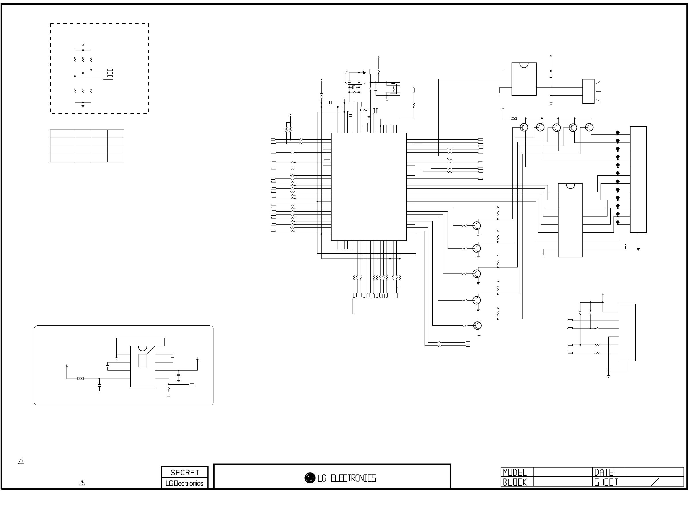
THE SYMBOL MARK OF THIS SCHEMETIC DIAGRAM INCORPORATES
SPECIAL FEATURES IMPORTANT FOR PROTECTION FROM X-RADIATION.
FILRE AND ELECTRICAL SHOCK HAZARDS, WHEN SERVICING IF IS
ESSENTIAL THAT ONLY MANUFATURES SPECFIED PARTS BE USED FOR
THE CRITICAL COMPONENTS IN THE SYMBOL MARK OF THE SCHEMETIC.
4.7K
R383
AMP_MUTE
NEC_RX
22
R397
EXT5V_CTRL
10K
R381
FLMD0
AMP_RESET
NEC_DBG_TX
NEC_IR
+3.5V_ST
+3.5V_ST
22R370
+5V_ST
2SA1504S
Q310
E
B
C
SCART1_MUTE
10K
R382
4.7K
R373
2SA1504S
Q308
E
B
C
22R350
PKLCS1212E4001-R1
BU300
1
2
22R331
OPT
22
R398
MICOM_RESET
EEPROM_SW
22R313
POWER_ON/OFF_1
22R327
+3.5V_ST
22uF
25V
3.3V to 5V
C303
10K
CLOCK
R303
22R346
TOOL1
UART_DBG_SW
4.7K
R372
22R328
+5V_ST
+5V_ST
0
R362
22R319
22R367
OPT
22R322
MICOM_RESET
POWER_DET
22R351
10K
R379
0R334
13pF
C305
TOOL0
4.7K
R371
22
R399
CEC_REMOTE_NEC
UART_SW2
10K
NON_CLOCK
R302
13pF
C307
4.7K
R384
RL_ON
22R325
22
OPT
R324
22R337
CLOCK_SDA
PANEL_CTL
BLM18PG121SN1D
L302
+5V_ST
MST_NEC_TX
22R366
22R344
MODEL1_OPT_2
10MHz
X300
47K
R352
22R332
FLMD0
22R329
CLOCK_SCL
MST_NEC_RX
+3.5V_ST
+3.5V_ST
2.2uF
10V
3.3V to 5V
C302
2SA1504S
Q309
E
B
C
JTP-1127WEM
SW300
12
43
22R357
22R368
TOOL0
22R321
OPT
IR_OUT_CTRL
22R369
2SA1504S
Q307
E
B
C
SIDE_HP_MUTE
THERMAL
SC632ULTRT
3.3V to 5V
IC300
3
C1-
2
C1+
4
IN
1
GND
5
EN
6
OUT
7
C2+
8
C2-
9
[EP]GND
22R316
NEC_TX
NEC_DBG_RX
2.2uF
10V
3.3V to 5V
C301
10K
R378
+3.5V_ST
LED_R/BUZZ
EXT_PWR_DET
22
OPT
R318
22R355
4.7K
R312
MODEL1_OPT_0
22R353
22R336
22R330
INV_CTL
22R354
4.7K
R310
KEY1
EXT12V_CTRL
2SA1504S
Q306
E
B
C
+5V_ST
22
OPT
R356
TOOL1
0
R361
22R323
BLM18PG600SN1D
L301
UART_SW1
22uF
25V
3.3V to 5V
C300
1M
R345
SUB_AMP_MUTE
+5V_ST
12507WS-06L
P300
1
2
3
4
5
6
7
22R365
KEY2
NEC_EEPROM_SCL
NEC_EEPROM_SDA
10KR333
OPT
DBG_SW
KID65003AF
IC303
3
I3
2
I2
4
I4
1
I1
6
I6
5
I5
7
I7
8
GND
9
COMMON
10
O7
11
O6
12
O5
13
O4
14
O3
15
O2
16
O1
22
R360
100K
R348
22R349
22R320
UPD78F1164GF(S)
NEC_MICOM
IC301
1
P60/SCL0
2
P61/SDA0
3
P62
4
P63
5
P31/TI03/TO03/INTP4
6
P64/RD
7
P65/WR0
8
P66/WR1
9
P67/ASTB
10
P77/EX23/KR7/INTP11
11
P76/EX22/KR6/INTP10
12
P75/EX21/KR5/INTP9
13
P74/EX20/KR4/INTP8
14
P73/EX19/KR3
15
P72/EX18/KR2
16
P71/EX17/KR1
17
P70/EX16/KR0
18
P06/WAIT
19
P05/CLKOUT
20
EVSS1
21
P80/EX0
22
P81/EX1
23
P82/EX2
24
P83/EX3
25
P84/EX4
26
P85/EX5
27
P86/EX6
28
P87/EX7
29
P30/INTP3/RTC1HZ
30
EVDD1
31
P50/EX8
32
P51/EX9
33
P52/EX10
34
P53/EX11
35
P54/EX12
36
P55/EX13
37
P56/EX14
38
P57/EX15
39
P17/EX31/TI02/TO02
40
P16/EX30/TI01/TO01/INTP5
41
P15/EX29/RTCDIV/RTCCL
42
P14/EX28/RXD3
43
P13/EX27/TXD3
44
P12/EX26/SO00/TXD0
45
P11/EX25/SI00/RXD0
46
P10/EX24/SCK00
47
AVREF1
48
P110/ANO0
49
P111/ANO1
50
AVREF0
51
AVSS
52
P157/ANI15
53
P156/ANI14
54
P155/ANI13
55
P154/ANI12
56
P153/ANI11
57
P152/ANI10
58
P151/ANI9
59
P150/ANI8
60
P27/ANI7
61
P26/ANI6
62
P25/ANI5
63
P24/ANI4
64
P23/ANI3
65
P22/ANI2
66
P21/ANI1
67
P20/ANI0
68
P130
69
P131/TI06/TO06
70
P04/SCK10/SCL10
71
P03/SI10/RXD1/SDA10
72
P02/SO10/TXD1
73
P01/TO00
74
P00/TI00
75
P145/TI07/TO07
76
P144/SO20/TXD2
77
P143/SI20/RXD2/SDA20
78
P142/SCK20/SCL20
79
P141/PCLBUZ1/INTP7
80
P140/PCLBUZ0/INTP6
81
P120/INTP0/EXLVI
82
P47/INTP2
83
P46/INTP1/TI05/TO05
84
P45/SO01
85
P44/SI01
86
P43/SCK01
87
P42/TI04/TO04
88
P41/TOOL1
89
P40/TOOL0
90
RESET
91
P124/XT2
92
P123/XT1
93
FLMD0
94
P122/X2/EXCLK
95
P121/X1
96
REGC
97
VSS
98
EVSS0
99
VDD
100
EVDD0
+3.5V_ST
22R326
10K
R358
4.7K
R374
22R347
74LX1G14CTR
IC302
3
GND
2
1A
4
1Y
1
NC
5
VCC
+3.5V_ST
2.2uF
10V
C308
10K
R380
BLM18PG600SN1D
3.3V to 5V
L300
4.7K
R376
+5V_ST
SOC_RESET
/PI_RESET_NEC
CEC_ON/OFF
12507WR-12L
P301
1
2
3
4
5
6
7
8
9
10
11
12
13
MODEL1_OPT_1
MODEL1_OPT_2
MODEL1_OPT_0
MODEL1_OPT_1
10K
OPT
R30810K
OPT
R309
10K
OPT
R31110K
OPT
R317
0.1uF
16V
C304
0.1uF
16V
C306
0.1uF
16V
C309
MMBT3904(NXP)
Q301
E
B
C
MMBT3904(NXP)
Q302
E
B
C
MMBT3904(NXP)
Q303
E
B
C
MMBT3904(NXP)
Q304
E
B
C
MMBT3904(NXP)
Q305
E
B
C
5V_ON/OFF
22R315
5V_ON/OFF
10K
R300
3.3V to 5V
SIGN190368
MODEL_OPT_3
MICOM MODEL OPTION
Closed to Crystal
Step Up regulator 3.3V to 5V(MAX 250mA)
MODEL OPTION
78
HIGH
80
MODEL_OPT_2
MODEL_OPT_0
PIN NAME
79MODEL_OPT_1
PIN NO. LOW
2011.08.21
3 20
EMEA INTERACTIVE
SUB MICOM
GP4_MSTAR
CLOCK
OPT
OPT OPT
OPT
NON_CLOCK
Can not use GPIO - P62,P63
Copyright © 2012 LG Electronics. Inc. All rights reserved.
Only for training and service purposes
LGE Internal Use Only
Page is loading ...
Page is loading ...
Page is loading ...
Page is loading ...
Page is loading ...
Page is loading ...
Page is loading ...
Page is loading ...
Page is loading ...
Page is loading ...
Page is loading ...
Page is loading ...
Page is loading ...
Page is loading ...
Page is loading ...
Page is loading ...
Page is loading ...
Page is loading ...
Page is loading ...
Page is loading ...
Page is loading ...
Page is loading ...
Page is loading ...
Page is loading ...
Page is loading ...
Page is loading ...
Page is loading ...
Page is loading ...
Page is loading ...
Page is loading ...
Page is loading ...
Page is loading ...
Page is loading ...
Page is loading ...
Page is loading ...
Page is loading ...
Page is loading ...
Page is loading ...
Page is loading ...
Page is loading ...
Page is loading ...
-
 1
1
-
 2
2
-
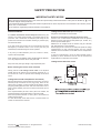 3
3
-
 4
4
-
 5
5
-
 6
6
-
 7
7
-
 8
8
-
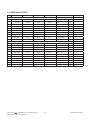 9
9
-
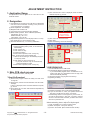 10
10
-
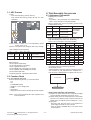 11
11
-
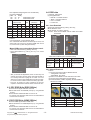 12
12
-
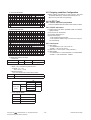 13
13
-
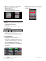 14
14
-
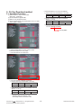 15
15
-
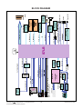 16
16
-
 17
17
-
 18
18
-
 19
19
-
 20
20
-
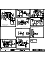 21
21
-
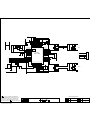 22
22
-
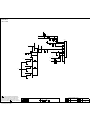 23
23
-
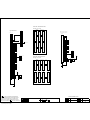 24
24
-
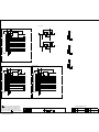 25
25
-
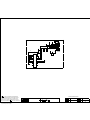 26
26
-
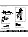 27
27
-
 28
28
-
 29
29
-
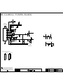 30
30
-
 31
31
-
 32
32
-
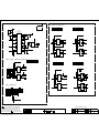 33
33
-
 34
34
-
 35
35
-
 36
36
-
 37
37
-
 38
38
-
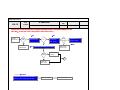 39
39
-
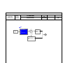 40
40
-
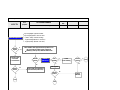 41
41
-
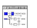 42
42
-
 43
43
-
 44
44
-
 45
45
-
 46
46
-
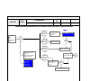 47
47
-
 48
48
-
 49
49
-
 50
50
-
 51
51
-
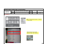 52
52
-
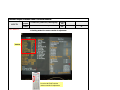 53
53
-
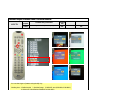 54
54
-
 55
55
-
 56
56
-
 57
57
-
 58
58
-
 59
59
-
 60
60
-
 61
61


Ask a question and I''ll find the answer in the document
Finding information in a document is now easier with AI
Related papers
Other documents
-
LG Electronics 47LN54**-Z* User manual
-
-
-
-
LG Electronics 42LM3450/345S/345T-ZA User manual
-
-
-
-
-